
 Open Access Article
 This Open Access Article is licensed under a Creative Commons Attribution-Non Commercial 3.0 Unported Licence
Tin(IV) dopant removal through anti-solvent engineering enabling tin based perovskite solar cells with high charge carrier mobilities†
R. M. I.
Bandara
 a,
K. D. G. I.
Jayawardena
a,
S. O.
Adeyemo
b,
S. J.
Hinder
c,
J. A.
Smith
d,
H. M.
Thirimanne
a,
N. C.
Wong
a,
F. M.
Amin
a,
B. G.
Freestone
d,
A. J.
Parnell
d,
D. G.
Lidzey
d,
H. J.
Joyce
b,
R. A.
Sporea
a and
S. R. P.
Silva
*a
a,
K. D. G. I.
Jayawardena
a,
S. O.
Adeyemo
b,
S. J.
Hinder
c,
J. A.
Smith
d,
H. M.
Thirimanne
a,
N. C.
Wong
a,
F. M.
Amin
a,
B. G.
Freestone
d,
A. J.
Parnell
d,
D. G.
Lidzey
d,
H. J.
Joyce
b,
R. A.
Sporea
a and
S. R. P.
Silva
*a
aAdvanced Technology Institute, Department of Electrical and Electronic Engineering, University of Surrey, Guildford, Surrey GU2 7XH, UK. E-mail: s.silva@surrey.ac.uk
bDivision of Electrical Engineering, Department of Engineering, University of Cambridge, 9 JJ Thomson Ave, Cambridge, CB3 0FA, UK
cThe Surface Analysis Laboratory, Faculty of Engineering and Physical Sciences, University of Surrey, Guildford GU2 7XH, UK
dDepartment of Physics and Astronomy, University of Sheffield, Hicks Building, Hounsfield Road, Sheffield S3 7RH, UK
First published on 25th June 2019
Abstract
We report the need for careful selection of anti-solvents for Sn-based perovskite solar cells fabricated through the commonly used anti-solvent method, compared to their Pb-based counterparts. This, in combination with the film processing conditions used, enables the complete removal of unwanted Sn4+ dopants, through engineering the anti-solvent method for Sn-based perovskites. Using a Cs0.05(FA0.83MA0.17)0.95Pb0.5Sn0.5I3 perovskite, charge carrier mobilities of 32 ± 3 cm2 V−1 s−1 (the highest reported for such systems through the optical-pump terahertz probe technique) together with ∼28 mA cm−2 short circuit current densities are achieved. A champion efficiency of 11.6% was obtained for solvent extraction using toluene (an 80% enhancement in efficiency compared to the other anti-solvents) which is further improved to 12.04% following optimised anti-solvent wash and thermal treatment. Our work highlights the importance of anti-solvents in managing defects for high efficiency low bandgap perovskite materials and develops the potential for all-perovskite tandem solar cells.
1. Introduction
Inorganic–organic hybrid metal halide perovskites have shown great promise in realising new materials for high performing photovoltaic (PV) devices with low fabrication cost.1–4 These perovskites possess a number of unique optoelectronic properties such as high light absorption, low Urbach energies, high charge carrier mobilities and high lifetimes, possessing high crystallinity even with low temperature processing, etc.2,5–7 allowing for the realisation of solution processed high performing optoelectronic devices. Emerging as strong competitors for current commercial silicon solar cells, single junction perovskite solar cells (PSC) have already achieved power conversion efficiencies (PCE) as high as 24.2%.8Recently, Lead-Tin mixed (LTM) perovskites have gained increasing attention due to the ability of tuning the bandgap to lower energies than those possible with Pb-only perovskites, which also enables tailored absorber layers to be fabricated for use as low bandgap cells in all-perovskite tandem solar cells.9–11 The first incorporation of Sn2+ in Pb2+ perovskites to fabricate a LTM planar PSC device was reported in 2014 by Jen and co-workers which yielded a PCE of 10.1%.12 By 2018, the efficiency of single junction LTM PSCs have reached 17.6% for MA0.4FA0.6Pb0.4Sn0.6I313 and MA0.5FA0.5Pb0.5Sn0.5I314 perovskite compositions.
One persistent issue limiting LTM PSCs performing to their maximum potential is the instability of Sn2+![[thin space (1/6-em)]](https://www.rsc.org/images/entities/char_2009.gif) 15,16 since Sn, is susceptible to oxidize into its more stable ionic form of Sn4+. Hence, Sn-based perovskites are highly sensitive to air and moisture. When in the perovskite matrix, this oxidation process is known to produce Sn vacancies which break the charge neutrality, thereby deteriorating the perovskite lattice.17 Furthermore, the Sn4+ ions act as p-type dopants in the perovskite film resulting in a “self-doping process”.18–20 These dopants play a major role in non-radiative recombination in Sn-based perovskites by acting as trap sites for mobile photo-generated charge carriers.15,21 Hence, reducing this oxidation process to enhance efficiencies in Sn-based PSCs has received much attention from the perovskite community.18 Generally, the incorporation of ≥50% of Pb2+,16 as well as a number of additives are used in the LTM perovskite precursors to slow down the oxidation process (which can still occur even under controlled conditions) with SnF2 being the most commonly used additive.16,18,22 Addition of SnF2–pyrazine complexes23 and ascorbic acid24 as antioxidants have also been reported. Interestingly, it has been reported that the extraction of Sn4+ from ionic mixtures for the determination of Sn4+ content in ores, alloys and food, is most effective when benzene, xylene or toluene is used as the diluent, used along with organic ligands.25 Incidentally, toluene is one of the widely used anti-solvents26,27 that enables the formation of pin-hole free absorber layers for high performing LTM perovskite PSCs,27,28 with other common anti-solvents being anisole,9,16 chlorobenzene,29 diethyl ether,22etc. Despite their widespread use, the impact of these anti-solvents is less well understood, especially with regards to their impact on the Sn-based systems as means to remove undesired dopants. Based on the above insights, we report efficient removal of Sn4+ from LTM perovskite absorber layers by careful selection of anti-solvents and optimal thermal treatment, to further enhance the performance of LTM perovskite devices using a triple-cation LTM perovskite with the composition of Cs0.05(FA0.83MA0.17)0.95Pb0.5Sn0.5I3 system as the absorber layer. Unlike their Pb-based counterparts, the anti-solvents show a significant impact on performance in Sn-based perovskite PVs. For the LTM perovskite PVs studied here, we show that the use of toluene enables larger grain sizes, but more importantly, better removal of Sn4+ resulting in enhancement in all the device parameters with a champion PCE of 11.62% in comparison to chlorobenzene (CB) and anisole (which are two other commonly used anti-solvents). The average PCE for toluene treated devices is improved by >80% compared to anisole treated devices, and improved by >60% in average PCE compared to CB treated devices. This is further supported by the observation of significantly lower Urbach tails and trap density when toluene is used as the anti-solvent. The charge carrier mobility of these perovskites is substantially increased by toluene treatment, reaching 32 ± 3 cm2 V−1 s−1, the highest reported so far with measurements based on Optical Pump – Terahertz Probe (OPTP) spectroscopy for Sn-based PSCs. Furthermore, the values achieved herein also strongly compete with those obtained for Pb only perovskites based on the OPTP technique. Following these findings, the fabrication conditions were further tuned enabling the complete removal of Sn4+ dopants, which to the best of our knowledge, is the first report of complete dopant removal in Sn based PSCs after fabrication of the absorber layer.
15,16 since Sn, is susceptible to oxidize into its more stable ionic form of Sn4+. Hence, Sn-based perovskites are highly sensitive to air and moisture. When in the perovskite matrix, this oxidation process is known to produce Sn vacancies which break the charge neutrality, thereby deteriorating the perovskite lattice.17 Furthermore, the Sn4+ ions act as p-type dopants in the perovskite film resulting in a “self-doping process”.18–20 These dopants play a major role in non-radiative recombination in Sn-based perovskites by acting as trap sites for mobile photo-generated charge carriers.15,21 Hence, reducing this oxidation process to enhance efficiencies in Sn-based PSCs has received much attention from the perovskite community.18 Generally, the incorporation of ≥50% of Pb2+,16 as well as a number of additives are used in the LTM perovskite precursors to slow down the oxidation process (which can still occur even under controlled conditions) with SnF2 being the most commonly used additive.16,18,22 Addition of SnF2–pyrazine complexes23 and ascorbic acid24 as antioxidants have also been reported. Interestingly, it has been reported that the extraction of Sn4+ from ionic mixtures for the determination of Sn4+ content in ores, alloys and food, is most effective when benzene, xylene or toluene is used as the diluent, used along with organic ligands.25 Incidentally, toluene is one of the widely used anti-solvents26,27 that enables the formation of pin-hole free absorber layers for high performing LTM perovskite PSCs,27,28 with other common anti-solvents being anisole,9,16 chlorobenzene,29 diethyl ether,22etc. Despite their widespread use, the impact of these anti-solvents is less well understood, especially with regards to their impact on the Sn-based systems as means to remove undesired dopants. Based on the above insights, we report efficient removal of Sn4+ from LTM perovskite absorber layers by careful selection of anti-solvents and optimal thermal treatment, to further enhance the performance of LTM perovskite devices using a triple-cation LTM perovskite with the composition of Cs0.05(FA0.83MA0.17)0.95Pb0.5Sn0.5I3 system as the absorber layer. Unlike their Pb-based counterparts, the anti-solvents show a significant impact on performance in Sn-based perovskite PVs. For the LTM perovskite PVs studied here, we show that the use of toluene enables larger grain sizes, but more importantly, better removal of Sn4+ resulting in enhancement in all the device parameters with a champion PCE of 11.62% in comparison to chlorobenzene (CB) and anisole (which are two other commonly used anti-solvents). The average PCE for toluene treated devices is improved by >80% compared to anisole treated devices, and improved by >60% in average PCE compared to CB treated devices. This is further supported by the observation of significantly lower Urbach tails and trap density when toluene is used as the anti-solvent. The charge carrier mobility of these perovskites is substantially increased by toluene treatment, reaching 32 ± 3 cm2 V−1 s−1, the highest reported so far with measurements based on Optical Pump – Terahertz Probe (OPTP) spectroscopy for Sn-based PSCs. Furthermore, the values achieved herein also strongly compete with those obtained for Pb only perovskites based on the OPTP technique. Following these findings, the fabrication conditions were further tuned enabling the complete removal of Sn4+ dopants, which to the best of our knowledge, is the first report of complete dopant removal in Sn based PSCs after fabrication of the absorber layer.
2. Results and discussion
2.1. Surface morphological properties of LTM perovskite films
For fabrication of the perovskite films, the LTM perovskite solution with an overall concentration of 1 M was prepared (SI-1, ESI,† for details). Thin films of this solution were cast via spin coating, inside a N2 filled glove box. 75 μl of the anti-solvent (CB, anisole or toluene) was dropped 5 s prior to the end of the spinning cycle, and the coated substrates were annealed at 70 °C for 20 min inside the glove box. Upon anti-solvent dropping, the perovskite layer changes colour from yellow to red-brown signifying the formation of a rich perovskite phase (Fig. 1(a)).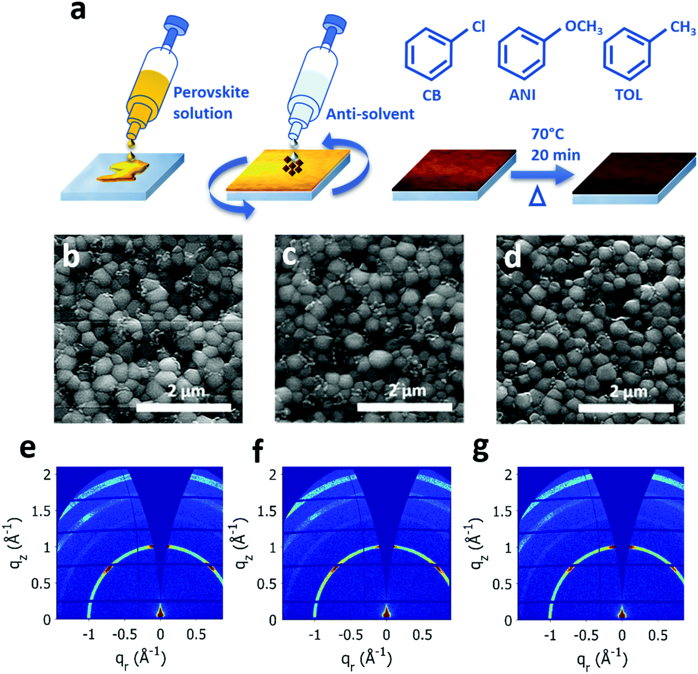 | ||
| Fig. 1 (a) The deposition and solvent engineering of the perovskite thin film. Chlorobenzene (CB), anisole (ANI) or toluene (TOL) as the anti-solvent (chemical structures shown) is dropped 5 s before the spin coating process of the perovskite solution is finished, aiding nucleation of perovskite phase. The red-brown perovskite thin film is then annealed at 70 °C for 20 min to complete film formation and remove solvent residue. Scanning electron microscopic images of as cast films treated with (b) chlorobenzene, (c) anisole and (d) toluene showing average grain sizes of 332.5 ± 21.14 nm for CB, 342.5 ± 29.43 nm for anisole and 387.5 ± 13.39 nm for toluene. 2D GIWAXS scattering patterns for (e) chlorobenzene, (f) anisole and (g) toluene treated LTM perovskites. | ||
The surface of perovskite thin films formed using the different anti-solvents were investigated through Scanning Electron Microscopy (SEM), and are depicted in Fig. 1(b)–(d). The average grain sizes (Fig. S1, ESI†) as given by the distributions are 332.5 ± 21.1 nm for CB, 342.5 ± 29.4 nm for anisole and 387.5 ± 13.4 nm for toluene, indicating that the largest grains are formed by toluene treatment with the smallest being produced by CB. We note that these grain sizes are comparable with Pb–Sn mixed perovskites reported in literature with a similar Pb:Sn ratio.22,30 In optoelectronic materials (including PSCs), the grain boundaries are one source of non-radiative recombination sites that can limit device performance.31 Therefore, the formation of larger grains through the use of toluene as an anti-solvent will decrease the grain boundary trap density. Furthermore, films formed using toluene as the anti-solvent demonstrate a more uniform distribution of grain sizes with the lowest spread of grain size data (FWHM of distribution 26.8 ± 4.3 nm) compared to the other two anti-solvents (FWHMCB = 42.3 ± 26.6 nm, FWHMANI = 58.9 ± 36.5 nm) which suggests a more homogenous nucleation process. To investigate the effect of different anti-solvents on the bulk crystal structure of LTM, grazing incidence wide angle X-ray scattering (GIWAXS) experiments were performed on the samples. The resulting 2D scattering patterns for annealed films quenched with different anti-solvents are depicted in Fig. 1(e)–(g). The corresponding diffraction peak positions (Fig. S2a, ESI†) observed for (100), (110), (111) and (200) perovskite scattering planes are identified. These are in good agreement with those reported in literature for triple cation perovskites32 and show no dependence on the anti-solvent used. In situ GIWAXS measurements were taken on as deposited films tracking the intensity of the (100) scattering peak during annealing and show that the perovskite phase is well formed prior to annealing (Fig. S2b, ESI†). In particular, the toluene quenched sample exhibits the highest proportion of post-annealing crystallinity before annealing, indicating the perovskite phase is initially more crystalline than for either anisole or CB treatment. Orientational analysis was performed on the GIWAXS data (Fig. S3, ESI†) and shows comparable texture and crystallinity for all treatments with the toluene sample showing some preferential out-of-plane orientation (see SI-3, ESI,† for details).
2.2. Effect of anti-solvents in Sn4+ removal
To identify the impact of the anti-solvent used on the removal of Sn4+, X-ray photoelectron spectroscopy (XPS) was carried out. The Sn2+ metal cations are observed at binding energies 486.40 ± 0.05 eV for Sn(3d5/2), 494.83 ± 0.06 eV for Sn(3d3/2) which are in good agreement with values reported in literature.33–35 Closer inspection of the aforementioned Sn peaks are observed to consist of shoulders at slightly higher binding energies (Fig. 2(a)) which, upon fitting with two Gaussians, were distinguished as Sn4+ peaks with binding energies of 487.57 ± 0.03 eV for Sn(3d5/2) and 496.29 ± 0.04 eV for Sn(3d3/2). The results extracted from the fittings for different anti-solvents are given in Table S1 (ESI†). When considering the surface metal ion composition, the atomic ratio of Pb2+A(%)/Sn2+A(%) gives 1.08, 0.79 and 0.77 for anisole (see SI-4, ESI,† for details), CB and toluene respectively (see Table S1, ESI†). This undoubtedly shows that while CB and toluene form nearly identical, Sn rich surface compositions, anisole treatment has formed a Pb2+ rich surface, as depicted in Fig. 2(b)(black). We have calculated the Sn4+A(%)/Sn2+A(%) based on the XPS measurements for different anti-solvents which is depicted in Fig. 2(b) (blue). It is clear that the lowest Sn4+ content is obtained from the films formed using toluene as the anti-solvent as opposed to when anisole and CB are used. This gives rise to a Sn4+A(%)/Sn2+A(%) of 0.36, 0.31 and 0.27 for anisole, CB and toluene respectively, decreasing the Sn4+ fraction.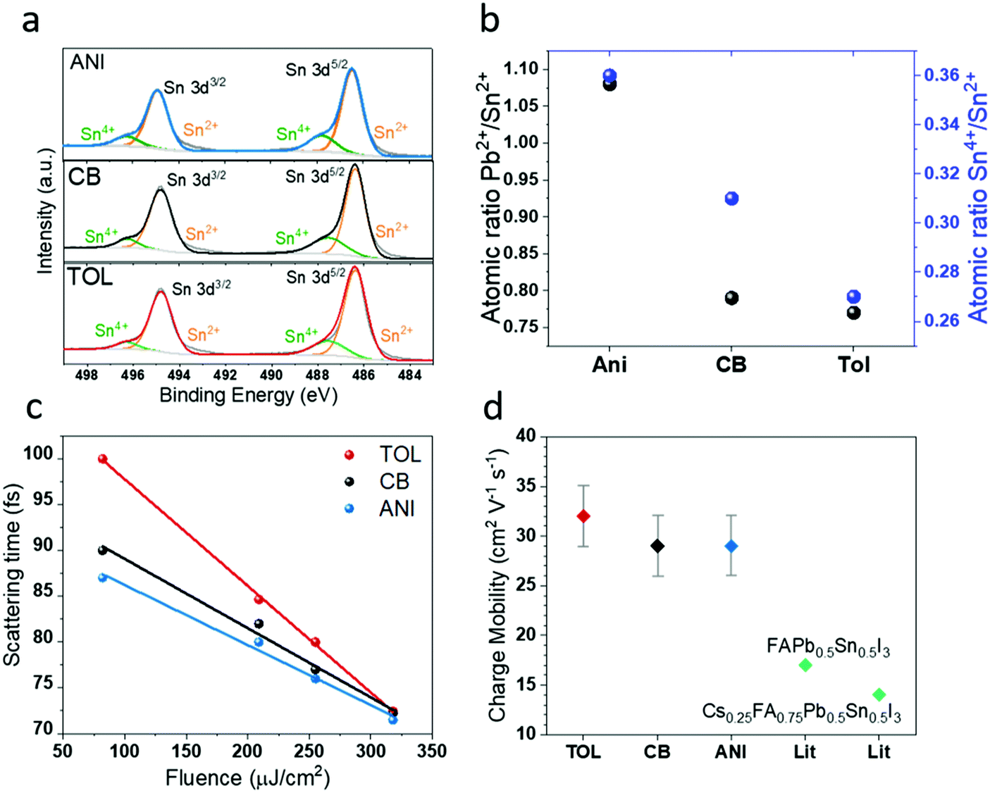 | ||
| Fig. 2 (a) The X-ray photoelectron spectra (XPS) for Sn species on the LTM perovskite surface for anisole (top), chlorobenzene (middle) and toluene (bottom) treatments. The Sn4+ peaks (green) are seen as shoulders at slightly higher binding energies with each of the main Sn2+ (3d) peaks (orange). (b) Atomic ratio of surface Sn4+/Sn2+ (blue) and Pb2+/Sn2+ (black) as derived from XPS measurements for different anti-solvent treatments. The lowest Sn4+/Sn2+ is seen for toluene treatment. (c) The scattering time (τ) plotted as a function of fluence for LTM layers with different anti-solvent treatments. Toluene treated perovskites show the highest τ at all fluences (consistent with the decrease in Sn4+ dopant scattering sites and the reduction in grain boundaries), while τ decreases with increasing fluence (consistent with increased carrier–carrier scattering under high injection conditions). Lowest τ is observed for anisole treatment in all cases. The lines are guides for the eye. (d) The charge carrier mobilities for LTM layers with different anti-solvents, where toluene shows the highest values and anisole the lowest, in comparison with the literature values determined by OPTP,36 for Pb–Sn mixed perovskite PSCs (the literature samples were treated with anisole). | ||
Next, we proceeded to study the effect of Sn4+ extraction on the charge carrier dynamics of the films by performing OPTP spectroscopy. The presence of Sn4+ traps in the perovskite film will act as recombination centres and in effect acts as an efficient quencher of the photo-generated electrons moving towards the ETL, through non-radiative recombination.37,38 When a single electron is trapped in a Sn4+ trap the charge neutrality is not achieved as it leaves a residual positive charge on the trap. The still prevailing positive charge in the trap Coulombically attracts more electrons leading to faster trap assisted recombination.38 The LTM perovskites, were photoexcited with a pump pulse wavelength of 950 nm with a duration of 35 fs and pump fluences between 82 and 320 μJ cm−2. The photoconductivity decays of all three solvent-treated samples were similar (see SI-5, ESI,† for details). However, the highest photoconductivity was observed for toluene treated LTMs followed by CB then anisole at all measured pump fluences (Fig. S5(a), ESI†). Analysis of the scattering times (τ) (Fig. 2(c)) indicates significantly longer scattering times for toluene treated LTMs compared to the other two, especially at lower fluences. The scattering time, we believe, is a direct correlation of the Sn4+ dopant concentration in Sn based perovkites,36 which act as scattering sites.36 Incidentally, these dopants are one of the major factors that hinder the charge carrier mobilities of Sn based perovskites.17 The larger grain sizes associated with the toluene treated LTMs would also reduce scattering at interfaces, further improving the mobility. The carrier mobility (μ) values (Fig. 2(d)), extracted from the transient THz conductivity measurement for toluene treatment was found to be on average 32 ± 3 cm2 V−1 s−1 and the high intra-grain mobility was found to be marginally improved by toluene treatment. The average μ values of CB and anisole treated LTMs were 29 ± 3 cm2 V−1 s−1. All mobility values have a standard deviation of less than 10%. These μ values, to the best of our knowledge are the highest achieved so far for Pb–Sn mixed PSCs and strongly compete with Pb only perovskites, as evident from values reported for Pb–Sn and Pb perovskites based on the OPTP technique (see Fig. S5(b), ESI†).
2.3. Impact of Sn4+ removal in PSC device performance
To test the impact of Sn4+ extraction, LTM PSCs were fabricated using the inverted (p-i-n) perovskite device architecture. The active area of these devices was 0.68 cm2 and illuminated under AM 1.5G solar spectrum through a large aperture area of 0.433 cm2. The current density–voltage relationship (J–V curves) for the champion device performances are depicted in Fig. 3(a), where it is clearly evident that LTM films formed using toluene as the anti-solvent yield higher values for Voc, Jsc and FF leading to higher PCE compared to the other two anti-solvents (see Table 1). The champion PCE of 11.62% is achieved for toluene, which is a significant improvement compared to the champion PCEs of 6.98% and 6.38% achieved for CB and anisole respectively. We note that in determining the Jsc values given here for our LTM PSCs we have used the integrated current from the EQE spectra in (Fig. 3(b)) to give a more accurate reading than those measured using halogen lamp based solar simulators.9 Here we obtain a very high >85% EQE for toluene treated LTMs. The distribution for the calculated Jsc values of LTM PSCs are given in Fig. 3(c) along with the other common device parameters, Voc (Fig. 3(d)), FF (Fig. 3(e)) and %PCE (Fig. 3(f)). The results clearly indicate that toluene treatment significantly improves all device parameters (while the lowest performance is seen in anisole treated LTM PSCs). By comparison, the Pb only analogue of this perovskite does not show a considerable change in device performance depending on the anti-solvent used as described in SI-6 (ESI†). We especially note the significant improvement for the Jsc, where the highest value observed is 28.05 mA cm−2 as opposed to the highest values of 22.10 mA cm−2 and 21.48 mA cm−2 for anisole and CB treated PSCs respectively. The average Jsc for toluene devices; 27.59 ± 0.32 mA cm−2, is a 32.96% improvement over anisole devices (20.75 ± 0.93 mA cm−2) and 30.63% improvement over CB devices (21.12 ± 0.56 mA cm−2). Similar trends were observed in Voc and FF, with the average Voc of toluene devices (0.62 ± 0.02 V) being 21.57% higher than that observed for anisole (0.51 ± 0.02 V) and 12.73% higher than that observed for CB (0.55 ± 0.01 V). The average FF of toluene (0.61 ± 0.03) is 10.91% and 8.93% improved over the devices fabricated using anisole (0.55 ± 0.03) and CB (0.56 ± 0.02) respectively. The resulting average PCEs depicted in Fig. 3(f) follow the trend, toluene (10.54 ± 0.63%) > CB (6.55 ± 0.36%) > anisole (5.82 ± 0.46%). The % improvement in average PCE of toluene treated devices is 81.10% and 60.92% compared to anisole and CB devices respectively. Furthermore, toluene treatment showed lower hysteresis in devices compared to the other two anti-solvents, as discussed in SI-7 (ESI†). These results are in good agreement with the previously discussed OPTP and XPS measurements, where toluene as anti-solvent results in more efficient removal of Sn4+ from the surface of the perovskite film than the other two anti-solvents leading to the LTM PSCs with the highest charge carrier mobilities and highest efficiencies. In comparison, CB treated perovskites layers containing more Sn4+ dopants have given rise to lower performing PSCs, and anisole treatment has resulted in the lowest device performance due to even higher Sn4+ content. However, even though anisole treatment is clearly seen to be unfavourable for our LTM PSCs, the devices have somewhat comparable performances with CB treated ones. Considering the increased Sn4+ dopants alone, anisole and CB devices could be expected to show a more noticeable difference in device performance, given that the Sn4+/Sn2+ consistently decreases from anisole to CB to toluene. A possible cause for the somewhat similar behaviour for devices fabricated using CB and anisole is the relatively high quantities of Pb2+ seen on the surface of anisole treated perovskite layers in the XPS study which may enable passivation of trap states.39,40 However, more specialised characterisation is required in order to identify how the increased surface Pb2+ impacts the interface and consequently overall device performance.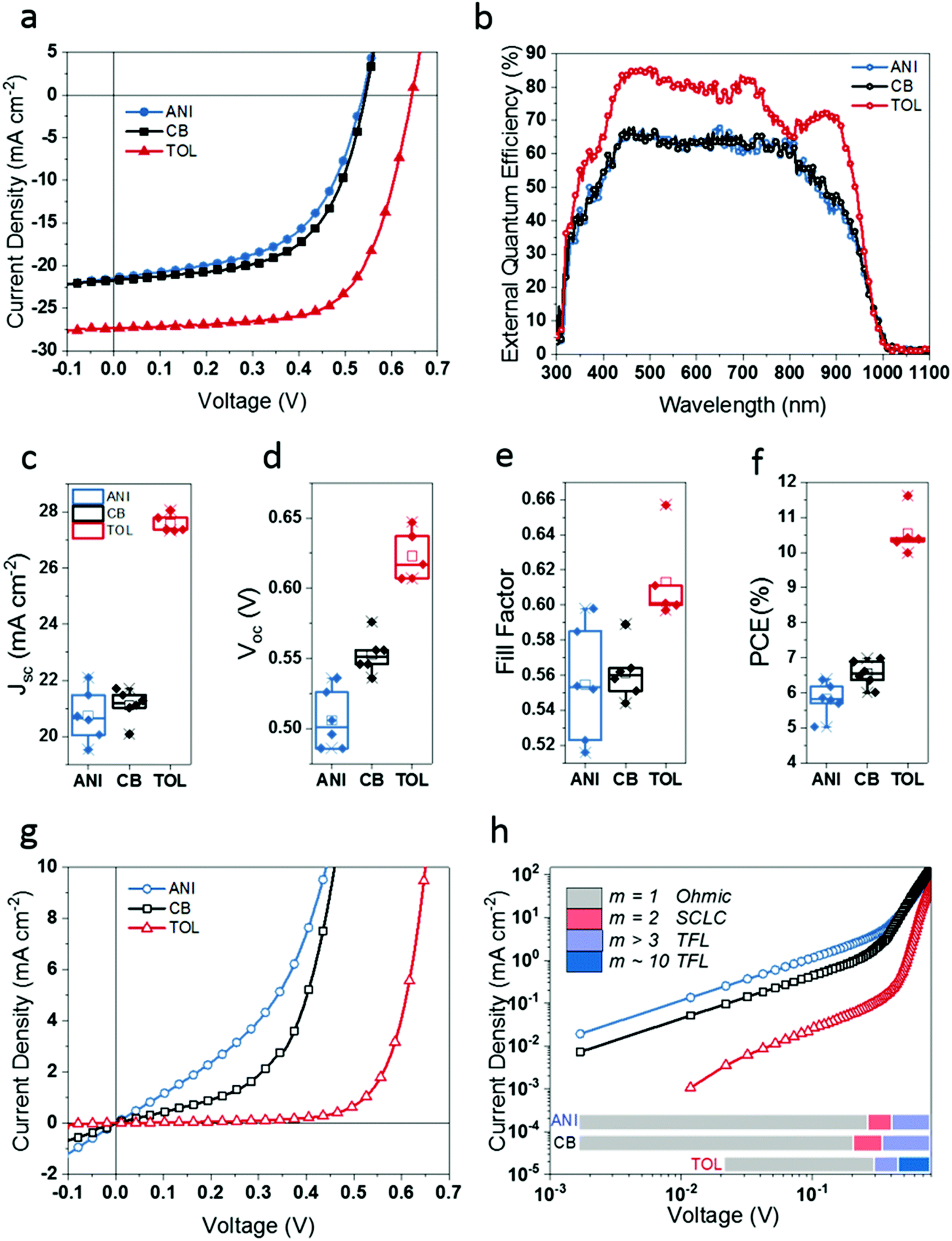 | ||
| Fig. 3 (a) The current density–voltage (J–V) behaviour of the champion LTM PSC devices for different anti-solvent treatments where toluene treatment clearly shows highest values for Voc, Jsc, FF (hence highest PCE) compared to the other two anti-solvents which give comparable device performances. (b) External quantum efficiencies (EQE) for the champion devices showing highest absorption for toluene treated devices. Box plots for (c) Jsc, (d) Voc (e) FF, and (f) %PCE of the LTM PSCs (n = 6), where the overall performance of toluene treated devices show nearly 70% average %PCE increase over the other two anti-solvent treated devices, and narrowest data spread. (g) The dark J–V characteristics of the above devices showing the least dark leakage current for a toluene treated device. (h) Plot of log(J) vs. log(V) for dark diode curves in (g), identifying the different charge transport regions. | ||
| Anti-solvent | Champion PCE (%) | PCE (%) | J sc (mA cm−2) | V oc (V) | Fill factor (FF) | Bandgap energy (eV) | Urbach energy (meV) |
|---|---|---|---|---|---|---|---|
| ANI | 6.38 | 5.82 ± 0.46 | 20.75 ± 0.93 | 0.51 ± 0.02 | 0.55 ± 0.03 | 1.269 ± 0.020 | 24.58 ± 0.04 |
| CB | 6.98 | 6.55 ± 0.36 | 21.12 ± 0.56 | 0.55 ± 0.01 | 0.56 ± 0.02 | 1.262 ± 0.013 | 25.13 ± 0.04 |
| TOL | 11.62 | 10.54 ± 0.63 | 27.59 ± 0.32 | 0.62 ± 0.02 | 0.61 ± 0.03 | 1.265 ± 0.020 | 21.21 ± 0.03 |
To elucidate the effect of anti-solvent on the band tails (occurring as a result of localised energy states in semiconducting materials41), the Urbach energies (EU), were calculated using the EQE spectra (see SI-8, ESI,† for detailed description). The lowest Urbach energy values were observed for toluene (EU = 21.21 ± 0.03 meV) treated samples (Table 1), attributed to the lowest band-tail defect states and higher crystalline order throughout the thickness of the sample. Anisole and CB treated LTMs gave comparable EU values of 24.58 ± 0.04 meV and 25.13 ± 0.04 meV respectively, resulting from a higher density of band tail defect states (due to the higher Sn4+) in these films. We note that the absorber layers processed using the different anti-solvents exhibit a similar bandgap of 1.26 eV (see SI-9, ESI†).
In order to further evaluate the impact of the Sn4+ removal process on the solar cell performance, we analysed the dark J–V curves of LTM PSCs. Careful inspection of the dark J–V curves (Fig. 3(g)) at negative voltages indicates that the dark leakage current of devices fabricated using CB and anisole are higher compared to the devices fabricated with toluene (0.64 mA cm−2, 1.32 mA cm−2 and ∼80 μA cm−2 at −0.1 V for CB, anisole and toluene respectively). Considering the devices’ dark characteristics (Fig. 3(h)), different charge transport regions can be identified, namely; Ohmic transport, space charge limited current (SCLC) and trap filled limit (TFL) (see SI-10, ESI,† for full analysis). In anisole and CB treated devices, the Ohmic regime is extended, as seen by the long initial region of constant slope (m) showing the quasi-Ohmic J–V behaviour (m = 1),42 which then gradually increases non-linearly through a region of m = 2, before reaching higher slopes expected for the TFL. Given that m = 2 corresponds to JSCLCshallowtraps, it can be concluded that CB and anisole treatments have resulted in shallow traps in the LTM PSC. Considering the voltage at which anisole and CB devices transfer from the Ohmic region to SCLC region (CB = 0.21 V, anisole = 0.27 V), the more prolonged quasi-Ohmic region of anisole devices suggest a higher trap density in these devices than that of CB ones. In the case of toluene treated devices, the Ohmic region is shorter than that of the other two anti-solvent treatments, and the slope quickly transfers to a region of m > 3 around 0.30 V followed by a prolonged region over which m ≈ 10 (beyond 0.46 V bias). This marks the TFL region where l > 2 of eqn (S10) (ESI†), and the trap dependent SCLC region (m ≈ 2) is hardly noticeable in this system. This rapid transition from Ohmic to TFL regime for toluene indicates that there are a reduced number of traps in this system, which is in agreement with the previous observations for the lower Sn4+ content (from the THz, XPS and photovoltaic device measurements).43VTFL increases in the order of toluene (0.30 V) < CB (0.35 V) < anisole (0.41 V) in the order of increasing trap density.44 In the TFL region, the slopes of CB and anisole dark curves reach m ≈ 4, which is in contrast to m ≈ 10 of toluene. We note that the trap free region (governed by Child's law) is not reached for any of the devices within the measured electric field range. The conclusion that this behaviour is caused by the higher number of parasitic charges brought upon by Sn4+ contamination for CB and anisole is further supported by recent literature where increased Sn vacancies were observed to give rise to a metal-like conductivity.42
2.4. Proposed hypotheses for Sn4+ removal mechanisms
Based on the results discussed above, it is evident that the removal of Sn4+ dopants from the LTM films during the fabrication process has the most significant impact on the performance of the LTM PSCs. The Sn4+ ions produced during fabrication and originally present in the SnI2 precursor are expected to exist in the system as SnI4, and we propose several hypotheses for the removal mechanisms of this compound which is detrimental to device performance. Firstly, SnI4 is a tetrahedral molecule (Fig. 4(a)) which, owing to its high symmetry, is non-polar in nature. Considering the relative polarities of the anti-solvents discussed (anisole = 0.198, CB = 0.188, toluene = 0.099) it can be seen that toluene is the least polar solvent. Given the non-polar nature of SnI4, it should therefore be most soluble in toluene. It is also the lightest of the three anti-solvents, with a molecular weight of 92.14 g mol−1 and has the lowest boiling point of 110.6 °C compared to 108.14 g mol−1 and 155.5 °C of anisole and 112.56 g ml−1 and 131.7 °C of CB.45 Hence, during the annealing process of the perovskite layer when the prevailing solvent is evaporated, the removal of SnI4 dissolved in the solvent can generally be considered higher with toluene.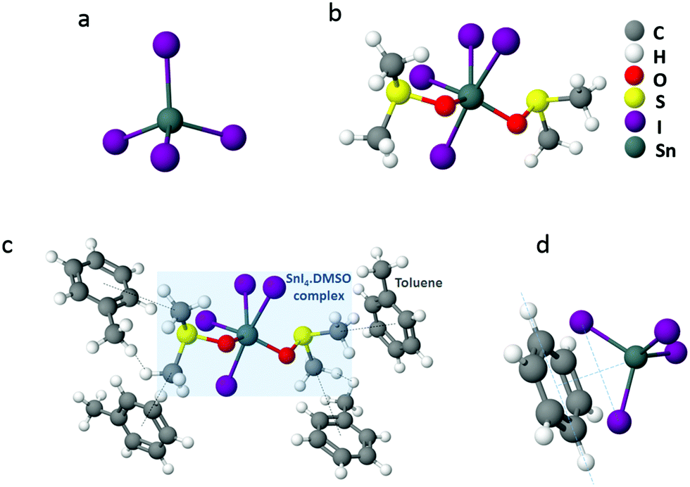 | ||
| Fig. 4 (a) Tetrahedral structure of SnI4. (b) Possible 6-coordinate complex formation of SnI4 with DMSO, where DMSO molecules act as ligands for the Sn4+ metal centre. (c) Possible interaction of SnI4·(DMSO)2 complex with non-polar toluene molecules. (The figures are not drawn to scale.) (d) The complex formation of SnI4 with non-polar aromatic molecules (benzene shown here as the aromatic molecule for the ease of the reader) as proposed by J. F. Murphy and D. E. Baker,48 where two of the iodine atoms of SnI4 are placed on the benzene ring, with the benzene plane lying parallel to a line drawn joining the iodine atoms. | ||
Furthermore, recent reports in the literature have described 6-coordinated complex formation of SnI4 with organic ligands resulting in complexes such as [SnI4(C5H5NO)2] and [SnI4{(C6H5)2SO}2].46 It has been shown in these studies that bonding occurs through coordination of electrons on the O atom of the ligand directly to the Sn centre of SnI4. Incidentally, the solvents used for the LTM precursor solution; DMF (C3H7NO) and DMSO (C2H6SO), which are known to act as common ligands for metal centres,47 are of similar nature to the ligands involved in the aforementioned complexes. Therefore, it can be hypothesised that similar co-ordination is viable in the LTM perovskite with DMF and DMSO. Fig. 4(b) depicts one possible complex that can be formed via DMSO ligand. If such bonding occurs, the more polar –CO and –SO groups would participate in bonding with SnI4, exposing the more non-polar C-H groups away from the SnI4 centre. It is then possible for these complexes to be solubilised in the non-polar toluene (Fig. 4(c)) and hence be removed from the perovskite crystal, via thermal annealing.
In addition to the above, early reports in chemical research suggest the dissolution of SnI4via complex formation in various organic solvents.48 Interestingly, it has been shown that with non-polar aromatic solvents such as benzene, toluene or xylene, there is a tendency for SnI4 to form a 1:1 (mole ratio) complex, through the occurrence of an acid–base like interaction, where SnI4 acts as a Lewis acid and the aromatic ring acts as the Lewis base.48 When the basicity of the aromatic ring increases, such as through the addition of methyl groups to the ring (i.e., benzene to toluene to xylene) the strength of the complex was found to be strengthened, hence increasing the solubility of SnI4 in the order of benzene < toluene < xylene. Considering the anti-solvents used herein, the low polarity of toluene solubilises SnI4 more easily enabling the formation of a complex in comparison to CB and anisole. Previous work indicates that two of the SnI4 iodine atoms participate in bonding with the aromatic group to make the SnI4·A (A = aromatic solvent molecule) complex where a line conjoining the iodine atoms lie in parallel to the plane of the ring (Fig. 4(d)).48 Due to the tetrahedral structure of SnI4, the Sn atom in the complex should be positioned directly over the six-fold centre of the aromatic group. Moreover, considering the previous reports, the formation of a SnI4·TOL complex with toluene can be suggested here, however it should be noted that the formation of this complex seems much less likely compared to the SnI4·DMSO complex hypothesised above. It is reasonable to speculate that complexing is initiated during the anti-solvent dripping stage, which is partially removed due to the high spin speed employed during the spin coating procedure. The remaining SnI4·TOL is easily removed during the annealing step, owing to the higher evaporation rate of toluene compared to the other two anti-solvents.
The removal of Sn4+ could happen via either of the hypothesised mechanisms, or a combination of them. Further in-depth experimental and simulation studies are currently in progress for the purpose of verifying the exact mechanism for Sn4+ removal and will be reported in a subsequent manuscript.
2.5. Solvent engineering and optimised thermal treatment for efficiency improvement
Following the understanding of this novel aspect of the anti-solvent engineering process, the fabrication process was further modified to promote complete removal of Sn4+ using toluene. This was carried out by changing physical parameters such as temperature and fine tuning the anti-solvent dripping procedure. Following recent reports on using higher annealing temperatures for FA and MA containing Pb–Sn mixed perovskites,22,27 we have used 120 °C as the annealing temperature for the modified system. Here we successfully facilitated the complete removal of Sn4+ as seen in the XPS spectra depicted in Fig. 5(a). The corresponding champion devices (Fig. 5(b)) showed ∼14% improvement in Voc, and 6% improvement on FF compared to the toluene treated champion reference device (Fig. 3) leading to higher PCE of 12.04%. The current density was calculated using the EQE profile for the device, shown in Fig. 5(c). In contrast to the other device parameters, the Jsc of these devices was observed to decrease. This can be attributed to the thickness variation of the LTM layer resulting from the post-treatments and Sn4+ removal. The thickness of the absorber layer is directly related to the quantity of light absorbed by the PSC, which in turn is related to the current output from the device. Hence, further improvements in Jsc are expected via optimisation of the absorber layer thickness.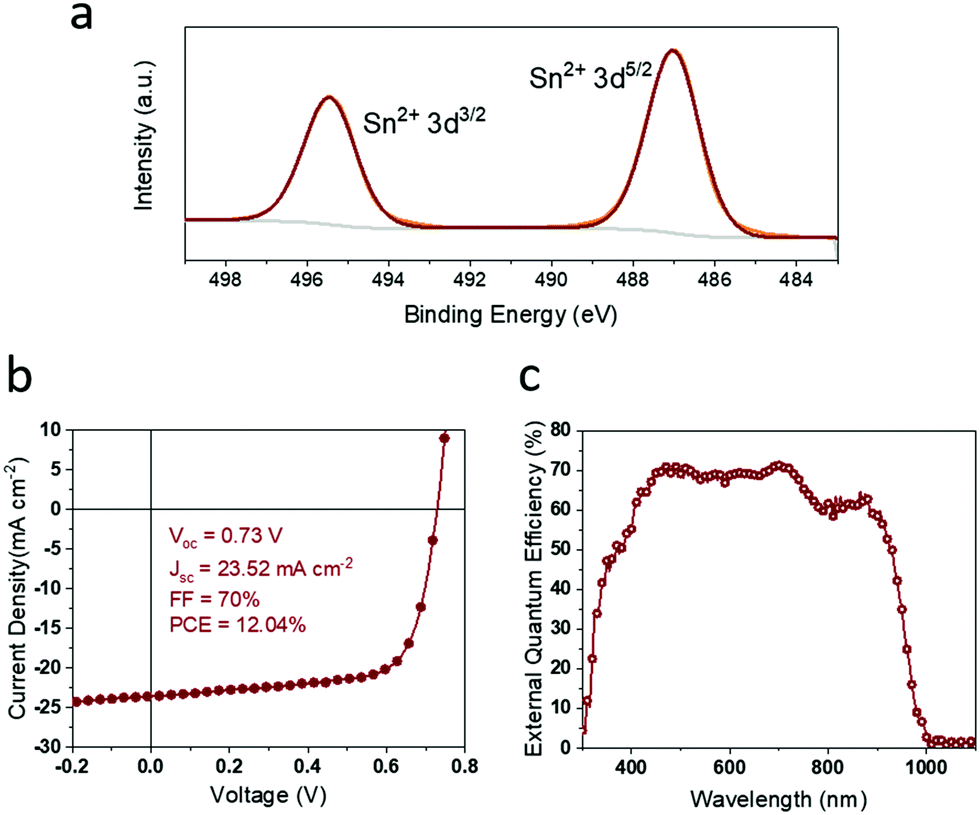 | ||
| Fig. 5 (a) The X-ray photoelectron spectra (XPS) for Sn species on the LTM perovskite surface after the modified solvent engineering process, showing Sn2+ peaks. No shoulders are seen in the peaks signifying the complete removal of Sn4+. The corresponding (b) champion J–V curve and device parameters, and (c) EQE resulted by the modified process. | ||
3. Conclusion
We report a new insight on the importance of careful selection of the anti-solvents for Sn-based perovskite PSCs. Compared to their Pb-only counterparts, the qualities of the anti-solvents used are observed to be more vital for the Sn-based perovskite PSC performance due to their impact on managing the Sn4+ defects of the absorber layers. Based on this, an approach for the complete removal of parasitic Sn4+ in Sn-based PSCs through solvent engineering is identified. The efficient extraction of Sn4+ from the perovskites was tested using a triple cation Pb–Sn mixed perovskite with the formula Cs0.05(FA0.83MA0.17)0.95Pb0.5Sn0.5I3. The results indicate that toluene acts as an efficient extraction medium for Sn4+, when used as an anti-solvent in the PSC fabrication process. Toluene treated LTM films not only show a lower Sn4+ quantity on the surface of the LTM films, but also show drastically improved PSC device parameters (Voc, Jsc, FF and PCE) compared to the other two anti-solvents examined; anisole and CB resulting in a champion PCE of 11.62%. The charge carrier mobilities reach 32 ± 3 cm2 V−1 s−1 with the toluene treatment which are the highest reported so far based on the OPTP technique for Sn based PSCs. The atomic percentage of Sn4+ decreases in the order of anisole > CB > toluene and the device performance increases in the order of anisole < CB < toluene which is further substantiated by the lower impact of parasitic charges for LTM PSCs under toluene treatment. Bandgap energies for all three LTM films were similar (∼1.26 eV) and the perovskite crystal structure of the thin films was found to be of similar nature, indicating that the major cause for the better device performance of toluene treated PSCs originates from the ability of toluene to remove Sn4+ dopants from the LTM film surface. These devices were further improved by fine tuning the device fabrication process to aid in complete removal of Sn4+ from the system. The Sn4+ extraction process outlined herein points towards higher efficiencies in tin based PSCs by simple modifications to the anti-solvent engineering route enabling further improvements for single junction Pb–Sn and Sn-only PSCs, as well as all perovskite multi-junction PVs.Conflicts of interest
There are no conflicts of interest to declare.Acknowledgements
R. M. I. B., K. D. I. J., H.M.T., R. A. S and S. R. P. S. gratefully acknowledge support from EPSRC via research grant EP/R025304/1 and the European Commission H2020 funded CORNET program (Grant agreement ID: 760949). R. M. I. B. acknowledges support from the University of Surrey Overseas Research Scholarship/University Research Scholarship. A. J. P. is grateful to Xenocs for their ongoing help and support in the user program at the University of Sheffield. H. J. J. acknowledges funding from the European Research Council (grant no. 716471, ACrossWire). SRPS acknowledges funding support from the Marcus Lee Foundation. We thank the Warwick Centre for Ultrafast Spectroscopy for access to experimental facilities.References
- M. M. Lee, J. Teuscher, T. Miyasaka, T. N. Murakami and H. J. Snaith, Efficient hybrid solar cells based on meso-superstructured organometal halide perovskites, Science, 2012, 338, 643–647 CrossRef CAS PubMed.
- M. A. Green, A. Ho-Baillie and H. J. Snaith, The emergence of perovskite solar cells, Nat. Photonics, 2014, 8, 506–514 CrossRef CAS.
- M. A. Green and A. Ho-Baillie, Perovskite Solar Cells: The Birth of a New Era in Photovoltaics, ACS Energy Lett., 2017, 2, 822–830 CrossRef CAS.
- M. Saliba, J.-P. Correa-Baena, M. Grätzel, A. Hagfeldt and A. Abate, Perovskite Solar Cells: From the Atomic Level to Film Quality and Device Performance, Angew. Chem., Int. Ed., 2018, 57, 2554–2569 CrossRef CAS PubMed; V. Ferguson, S. R. P. Silva and W. Zhang, Carbon Materials in Perovskite Solar Cells: Prospects and Future Challenges, Energy Environ. Mater., 2019 DOI:10.1002/eem2.12035.
- C. Katan, A. D. Mohite and J. Even, Entropy in halide perovskites, Nat. Mater., 2018, 17, 377–379 CrossRef CAS PubMed.
- H. J. Snaith, Present status and future prospects of perovskite photovoltaics, Nat. Mater., 2018, 17, 372–376 CrossRef CAS PubMed.
- S. Shi, Y. Li, X. Li and H. Wang, Advancements in all-solid-state hybrid solar cells based on organometal halide perovskites, Mater. Horiz., 2015, 2, 378–405 RSC.
- Best research-cell efficiencies, https://www.nrel.gov/pv/assets/images/efficiency-chart-20180716.jpg, accessed: April 2019.
- G. E. Eperon, et al., Perovskite-perovskite tandem photovoltaics with optimised band gaps, Science, 2016, 354, 861–865 CrossRef CAS PubMed.
- B. Zhao, et al., High Open-Circuit Voltages in Tin-Rich Low-Bandgap Perovskite-Based Planar Heterojunction Photovoltaics, Adv. Mater., 2017, 29, 1604744 CrossRef PubMed.
- R. Prasanna, et al., Band Gap Tuning via Lattice Contraction and Octahedral Tilting in Perovskite Materials for Photovoltaics, J. Am. Chem. Soc., 2017, 139, 11117–11124 CrossRef CAS PubMed.
- F. Zuo, et al., Binary-Metal Perovskites Toward High-Performance Planar-Heterojunction Hybrid Solar Cells, Adv. Mater., 2014, 26, 6454–6460 CrossRef CAS PubMed.
- D. Zhao, et al., Low-bandgap mixed tin–lead iodide perovskite absorbers with long carrier lifetimes for all-perovskite tandem solar cells, Nat. Energy, 2017, 2, 17018 CrossRef CAS.
- G. Kapil, et al., Highly Efficient 17.6% Tin–Lead Mixed Perovskite Solar Cells Realised through Spike Structure, Nano Lett., 2018, 18, 3600–3607 CrossRef CAS PubMed.
- J. Fan, et al., Molecular Self-Assembly Fabrication and Carrier Dynamics of Stable and Efficient CH3NH3Pb(1−x)SnxI3 Perovskite Solar Cells, ChemSusChem, 2017, 10, 3839–3845 CrossRef CAS PubMed.
- T. Leijtens, R. Prasanna, A. Gold-Parker, M. F. Toney and M. D. McGehee, Mechanism of Tin Oxidation and Stabilisation by Lead Substitution in Tin Halide Perovskites, ACS Energy Lett., 2017, 2, 2159–2165 CrossRef CAS.
- N. K. Noel, et al., Lead-free organic–inorganic tin halide perovskites for photovoltaic applications, Energy Environ. Sci., 2014, 7, 3061–3068 RSC.
- S. Gupta, D. Cahen and G. Hodes, How SnF2 Impacts the Material Properties of Lead-Free Tin Perovskites, J. Phys. Chem. C, 2018, 122, 13926–13936 CrossRef CAS.
- N. K. Noel, et al., Lead-free organic–inorganic tin halide perovskites for photovoltaic applications, Energy Environ. Sci., 2014, 7, 3061–3068 RSC.
- Y. Takahashi, et al., Charge-transport in tin-iodide perovskite CH3NH3SnI3: origin of high conductivity, Dalton Trans., 2011, 40, 5563 RSC.
- K. Yamada, et al., Anomalous Dielectric Behavior of a Pb/Sn Perovskite: Effect of Trapped Charges on Complex Photoconductivity, ACS Photonics, 2018, 5, 3189–3197 CrossRef.
- W. Liao, et al., Fabrication of Efficient Low-Bandgap Perovskite Solar Cells by Combining Formamidinium Tin Iodide with Methylammonium Lead Iodide, J. Am. Chem. Soc., 2016, 138, 12360–12363 CrossRef CAS PubMed.
- S. J. Lee, et al., Fabrication of Efficient Formamidinium Tin Iodide Perovskite Solar Cells through SnF2 –Pyrazine Complex, J. Am. Chem. Soc., 2016, 138, 3974–3977 CrossRef CAS PubMed.
- X. Xu, et al., Ascorbic acid as an effective antioxidant additive to enhance the efficiency and stability of Pb/Sn-based binary perovskite solar cells, Nano Energy, 2017, 34, 392–398 CrossRef CAS.
- B. M. Sargar and M. A. Anuse, Rapid Solvent Extraction of Tin(IV) with High Molecular Weight Amine from Hydrochloric Acid Solution, J. Chin. Chem. Soc., 2003, 50, 841–848 CrossRef CAS.
- Z. Yang, et al., Stable Low-Bandgap Pb–Sn Binary Perovskites for Tandem Solar Cells, Adv. Mater., 2016, 28, 8990–8997 CrossRef CAS PubMed.
- A. Rajagopal, et al., Highly Efficient Perovskite-Perovskite Tandem Solar Cells Reaching 80% of the Theoretical Limit in Photovoltage, Adv. Mater., 2017, 29, 1702140 CrossRef PubMed.
- X. Liu, et al., Improved efficiency and stability of Pb–Sn binary perovskite solar cells by Cs substitution, J. Mater. Chem. A, 2016, 4, 17939–17945 RSC.
- M. Lyu, et al., Highly compact and uniform CH3NH3Sn0.5Pb0.5I3 films for efficient panchromatic planar perovskite solar cells, Sci. Bull., 2016, 61, 1558–1562 CrossRef CAS.
- G. E. Eperon, et al., Perovskite-perovskite tandem photovoltaics with optimised band gaps, Science, 2016, 354, 861–865 CrossRef CAS PubMed.
- T. S. Sherkar, C. Momblona, L. Gil-Escrig, H. J. Bolink and L. J. A. Koster, Improving Perovskite Solar Cells: Insights From a Validated Device Model, Adv. Energy Mater., 2017, 7, 1602432 CrossRef.
- H. Tsai, et al., Light-induced lattice expansion leads to high-efficiency perovskite solar cells, Science, 2018, 360, 67–70 CrossRef CAS PubMed.
- NIST XPS Database, Selected Element Search Menu. Available at: https://srdata.nist.gov/xps/selEnergyType.aspx, accessed: 1st August 2018.
- T.-B. Song, et al., Importance of Reducing Vapor Atmosphere in the Fabrication of Tin-Based Perovskite Solar Cells, J. Am. Chem. Soc., 2017, 139, 836–842 CrossRef CAS PubMed.
- M. A. Stranick and A. Moskwa, SnO by XPS, Surf. Sci. Spectra, 1993, 2, 45–49 CrossRef CAS.
- L. M. Herz, Charge-Carrier Mobilities in Metal Halide Perovskites: Fundamental Mechanisms and Limits, ACS Energy Lett., 2017, 2, 1539–1548 CrossRef CAS.
- M. A. Green, Solar cells: operating principles, technology, and system applications, Prentice-Hall, 1982 Search PubMed.
- T. S. Sherkar, et al., Recombination in Perovskite Solar Cells: Significance of Grain Boundaries, Interface Traps, and Defect Ions, ACS Energy Lett., 2017, 2, 1214–1222 CrossRef CAS PubMed.
- Q. Chen, et al., Controllable Self-Induced Passivation of Hybrid Lead Iodide Perovskites toward High Performance Solar Cells, Nano Lett., 2014, 14, 4158–4163 CrossRef CAS PubMed.
- G. A. MacDonald, et al., Methylammonium lead iodide grain boundaries exhibit depth-dependent electrical properties, Energy Environ. Sci., 2016, 9, 3642–3649 RSC.
- A. S. Hassanien and A. A. Akl, Influence of composition on optical and dispersion parameters of thermally evaporated non-crystalline Cd50S50−xSex thin films, J. Alloys Compd., 2015, 648, 280–290 CrossRef CAS.
- Y. Zong, Z. Zhou, M. Chen, N. P. Padture and Y. Zhou, Lewis-Adduct Mediated Grain-Boundary Functionalisation for Efficient Ideal-Bandgap Perovskite Solar Cells with Superior Stability, Adv. Energy Mater., 2018, 8, 1800997 CrossRef.
- D. Shi, et al., Solar cells. Low trap-state density and long carrier diffusion in organolead trihalide perovskite single crystals, Science, 2015, 347, 519–522 CrossRef CAS PubMed.
- N. A. Nismy, K. D. G. I. Jayawardena, A. A. D. T. Adikaari and S. R. P. Silva, Nano-engineering of hybrid organic heterojunctions with carbon nanotubes to improve photovoltaic performance, Org. Electron., 2015, 22, 35–39 CrossRef CAS.
- The PubChem Project. Available at: https://pubchem.ncbi.nlm.nih.gov/, accessed: 26th September 2018.
- E. Wlaźlak, W. Macyk, W. Nitek and K. Szaciłowski, Influence of π-Iodide Intermolecular Interactions on Electronic Properties of Tin(IV) Iodide Semiconducting Complexes, Inorg. Chem., 2016, 55, 5935–5945 CrossRef PubMed.
- M. Ozaki, et al., Solvent-Coordinated Tin Halide Complexes as Purified Precursors for Tin-Based Perovskites, ACS Omega, 2017, 2, 7016–7021 CrossRef CAS.
- J. F. Murphy and D. E. Baker, Complexes of Stannic Iodide with Aromatic Hydrocarbons, Can. J. Chem., 1965, 43, 1272–1278 CrossRef.
Footnote |
| † Electronic supplementary information (ESI) available. See DOI: 10.1039/c9tc02003a |
| This journal is © The Royal Society of Chemistry 2019 |