
 Open Access Article
 This Open Access Article is licensed under a
 Creative Commons Attribution 3.0 Unported Licence
Alkyl chain assisted thin film growth of 2,7-dioctyloxy-benzothienobenzothiophene†
Harald
Spreitzer
a,
Benjamin
Kaufmann
b,
Christian
Ruzié
c,
Christian
Röthel
a,
Thomas
Arnold
 defg,
Yves H.
Geerts
c,
Christian
Teichert
b,
Roland
Resel
*a and
Andrew O. F.
Jones
ah
defg,
Yves H.
Geerts
c,
Christian
Teichert
b,
Roland
Resel
*a and
Andrew O. F.
Jones
ah
aInstitut für Festkörperphysik, Technische Universität Graz, Petersgasse 16, 8010 Graz, Austria. E-mail: roland.resel@tugraz.at
bInstitut für Physik, Montanuniversität Leoben, 8700 Leoben, Austria
cLaboratoire de Chimie des Polymères, Faculté des Sciences, Université Libre de Bruxelles (ULB), CP206/01, Campus de la Plaine, 1050 Brussels, Belgium
dDepartment of Chemistry, University Bath, England, Claverton Down, Bath, BA2 7AY, England, UK
eISIS Neutron and Muon Source, Science and Technology Facilities Council Rutherford Appleton Laboratory, Didcot, OX11 0QX, UK
fDiamond Light Source Ltd., Harwell Science and Innovation Campus, Didcot OX11 0DE, UK
gEuropean Spallation Source ERIC, P.O. Box 176, SE-221 00 Lund, Sweden
hAnton Paar GmbH, Anton-Paar-Straße 20, 8054 Graz, Austria
First published on 24th June 2019
Abstract
An understanding of the thin film growth modes of substrate-induced polymorphs allows a deeper insight into the origin of this class of materials. Their onset of crystallisation, the subsequent crystal growth, the evolution of the thin film morphology and the transfer to the equilibrium bulk structure are still not fully understood. This work investigates the thin film formation of a conjugated molecule with terminal alkyl chains. Thin films of 2,7-dioctyloxy[1]benzothieno[3,2-b]benzothiophene were grown by physical vapor deposition on silicon oxide surfaces with varying the film thicknesses from the sub-monolayer regime up to 33 layer thick films. Additionally, the substrate temperature and deposition rate were varied. The films were investigated by atomic force microscopy, X-ray reflectivity and grazing incidence X-ray diffraction. The first growth stage is a closed monolayer with a thickness of 3 nm formed by upright-standing molecules. It is found that the substrate-induced crystal structure is already formed within the first monolayer and continues its growth up to the largest investigated film thickness. The characteristic morphology is terraced islands over the whole thickness range. On top of the first monolayer a morphology with several terrace levels appears, which is associated with a rapid increase of the surface roughness. At larger film thicknesses (≥13 nm) the number of terrace steps does not increase significantly, so that the surface roughness only increases slowly. This work shows that molecules with terminal alkyl chains can form a substrate-induced phase up to large film thicknesses without the appearance of the equilibrium bulk phase.
Introduction
In the field of organic semiconductors, charge-transport capability is dependent on the molecular and crystalline structure, making the knowledge and control of the molecular packing a key aspect in improving device performance. This is particularly important in layers close to the substrate where the majority of charge transport takes place, for example in organic field-effect transistors. Due to the presence of the flat surface, the substrate often induces a different polymorphic phase to the bulk structure, a so-called substrate-induced phase (SIP).1,2 Despite the fact that these structures are often less energetically favourable than the single-crystal or bulk structure, they can be stabilized close to the substrate surface. The formation of a substrate-induced phase starting from the first monolayers has already been studied for different thin film preparation techniques such as spin coating and physical vapor deposition.3–7 However, detailed studies on the formation of a substrate-induced phase for a molecule with flexible side chains are still rare.6,7 In most cases, a pronounced layer-plus-island growth mode is found where at first the formation of a closed monolayer is observed which is followed by the formation of islands (Stranski–Krastanov growth).8–10 In the case of organic molecules where intermolecular interactions dominate over the molecule–substrate interactions, e.g. hydrogen bonded dye molecules, distinct island formation – island growth mode or Vollmer–Weber growth – is observed.11 A defined layer-by-layer growth (Frank–van der Merwe growth) is only observed in rare cases, e.g. within the first mono-layers close to the substrate surface, at phase transitions to liquid crystalline states, or where bimodal growth is established.12–15Recently it has been observed that benzothienobenzothiophene (BTBT) based molecules show excellent transistor performance within thin films.16 The control of the crystal structure by thermal processing is a key factor for their successful use, since liquid crystalline states and soft crystal phases are present in this class of molecules.17,18 Additionally, the thin film morphology is of fundamental importance, since homogenous films with low surface roughness provide defined and optimized conditions for charge transport.19,20
In this work, the film formation of a substrate-induced phase formed by physical vapor deposition of 2,7-dioctyloxy[1]benzothieno[3,2-b]benzothiophene (C8O-BTBT-OC8) is investigated under different deposition conditions and for different film thicknesses. Furthermore, its film formation properties and film morphologies are determined. Previous studies on spin coated films of C8O-BTBT-OC8 demonstrated that it forms a SIP in thin films converting to the bulk structure over time or by solvent vapor annealing.21 Interestingly, the SIP shows a fundamentally different type of molecular packing than the bulk crystal structure. While denser bulk crystals are layered with slipped π–π stacking of the aromatic cores and interdigitation of the molecules, the SIP shows a herringbone packing of the aromatic cores.22 A schematic picture of the packing of the molecules within the SIP is shown in Fig. 1, the full crystal structure information is available from the CSD database under the entry 1557531. Within this paper, we focus on the formation of a substrate-induced phase starting from the first monolayers together with the evolution of the thin film morphology as the film thickness is increased up to 99 nm.
 | ||
| Fig. 1 Packing of the C8O-BTBT-OC8 molecule within the substrate-induced phase in a front view along the c-axis (a) and in a side view along [011] (b). The crystallographic unit cell is drawn by green lines, additionally the (100) plane is drawn by thick black lines. | ||
Experimental
2,7-Dioctyloxy[1]benzothieno[3,2-b]benzothiophene (C8O-BTBT-OC8) was synthesized following the previously reported procedure.23 Silicon wafers with a 150 nm thermally grown oxide layer were used as substrates. Before deposition, the wafers were cleaned first with acetone and then isopropanol in an ultrasonic bath (15 minutes in each solvent) and dried with CO2 gas. Within the vacuum chamber the substrates were sputtered with Ar+ ions at a pressure of 5 × 10⁻⁵ mbar for 10 minutes. The molecule C8O-BTBT-OC8 was filled in a steel Knudsen cell and deposited onto the substrates by physical vapor deposition at a base pressure of 1 × 10⁻⁷ mbar. Films with different nominal thicknesses, from the sub-monolayer regime up to multilayers with thicknesses of 99 nm, were prepared; the amount of deposited material was determined by a quartz micro balance. Based on our ex situ analysis of film thickness we found a frequency shift of 30 Hz nm−1. Films were prepared at different deposition conditions fixing the substrate temperature either at room temperature or at 75 °C and the deposition rate (DR) either at 0.15 nm min−1 or at 1.2 nm min−1.Atomic Force Microscopy (AFM) measurements were performed with a Multi-Mode IIIa-AFM from Digital Instruments in tapping mode under ambient conditions. NSG30 cantilevers from NT-MDT made of single crystal silicon with a tip curvature radius of 6 nm and an opening angle at the apex of less than 10° were used. The cantilevers had resonant frequencies ranging from 320–361 kHz and typical force constants of 40 N m−1. For AFM image analysis, the software Gwyddion was used.24 Height distribution functions (ρ) are plotted as a function of the z-coordinate (perpendicular to the sample surface) with the origin at the lowest observed z – height. The surface roughness was determined in two ways; either directly from the height scan and and/or from fitted height–height correlation functions using different details of the micrographs. Error estimations were performed by investigation of different areas of the AFM images and taking the standard deviation.
Specular X-ray reflectivity (XRR) measurements were performed using a PANalytical Empyrean reflectometer. The primary side was equipped with a copper sealed tube for Kα radiation (λ = 0.15418 nm), a 1/32° divergence slit, 4 mm beam mask and a multilayer mirror for a monochromatic and parallel beam. The secondary side consisted of a 0.1 mm receiving slit and a 0.02 rad Soller slit together with a PANalytical PIXcel3D detector. The intensity of the X-ray reflectivity data is plotted as a function of the out-of-plane scattering vector qz, where qz = 4π/λsin(2Θ/2), with 2Θ being the scattering angle and λ the wavelength of the radiation used. For films of sub-monolayers up to thin multilayers (up to 5 nm nominal thickness), the data were fitted using the software Stochfit to determine an electron density distribution across the film thickness using a model free approach.25 For thicker films (starting from 13 nm thickness), the X’Pert Reflectivity software package (PANalytical) was used to fit the reflectivity data, the electron density modulation from the crystal structure was used in the model fit.
Grazing incidence X-ray diffraction (GIXD) measurements were performed at the Diamond Light Source (Didcot, UK) on beamline I07.26 X-rays with a wavelength of 0.0992 nm (12.5 keV) were used at an incident angle of 0.12°, slightly below the critical angle of total external reflection of the substrate to reduce the background signal. The exposure time was varied from 5 to 300 seconds, depending on the intensity of the diffracted signal as a function of the different film thicknesses. Diffracted intensities were measured using a Pilatus 2 M area detector (Dectris). Reciprocal space maps were calculated from the measured data using the xrayutilities library for Python.27 The reciprocal space maps are compared with calculated diffraction patterns based on the SIP crystal structure of C8O-BTBT-OC8 by using the software PyGID.28
Results
A Atomic force microscopy
In a first step, the thin film formation was investigated in the monolayer regime. Fig. 2 shows AFM micrographs of sub-monolayers with ∼50% coverage prepared under different conditions. The films show islands with a constant height of 3.1 nm. This length is slightly smaller than the length of the elongated molecule; a value of 3.0 nm is observed for the molecular conformation present in the known crystal structures.21 The lateral island size becomes larger when the substrate temperature is elevated during the deposition process (Fig. 2b) and becomes smaller when an increased deposition rate is used (Fig. 2c). Comparison of the observed morphology to other BTBT derivatives reveals similar island sizes, but a slightly different island shape.29,30 The observed island sizes can be readily explained: (a) a larger island size at 75 °C substrate temperature is due to an enhanced ability of the molecules to migrate across the substrate surface and (b) a smaller island size at higher deposition rates is due to an increased nucleation rate of islands.10 | ||
| Fig. 2 Atomic force microscopy images of sub-monolayers with a coverage of about 50% prepared on silicon oxide surfaces (a) at room temperature with a low deposition rate (0.15 nm min−1), (b) at a substrate temperature of 75 °C with low deposition rate and (c) at room temperature with a high deposition rate (1.2 nm min−1). The z-scales are 10 nm. | ||
In a subsequent step, the evolution of the thin film morphology was investigated as a function of nominal film thickness. Starting with a thickness of 3.3 nm, a closed first monolayer is observed (Fig. 3a). The second monolayer starts to form flat islands with an island height of 3 nm as can be clearly seen by the height distribution function (Fig. 3e). At a nominal film thickness of 5 nm the formation of a terrace like structure is found (Fig. 3b) where three different terrace levels can be observed. Increasing the film thickness to 13 nm (Fig. 3c) still results in a terraced morphology. Height distribution analysis reveals three dominant terrace levels with step heights of between 2.8 nm and 3.1 nm (Fig. 3g). The terraced structure is also present in a film with a thickness of 99 nm (Fig. 3d), here four primary terrace levels are observed. Increasing the substrate temperature during the film deposition process results in similar terrace-like morphologies with a similar increase of terrace levels with film thickness (Fig. S1, ESI†). However, the lateral extension of the terraces increases considerably with increasing film thickness.
 | ||
| Fig. 3 Atomic force microscopy images and height distribution functions of C8O-BTBT-OC8 films prepared at room temperature at low deposition rates (0.15 nm min−1) with different nominal thicknesses of (a and e) 3.3 nm (1.1 monolayers), (b and f) 5 nm (1.6 monolayers), (c and g) 13 nm (4.3 monolayers) and (d and h) 99 nm (33 monolayers). The z-scale of the images (a–d) is 20 nm. | ||
The observed evolution in the thin film morphology can be compared to the film formation of other rod-like conjugated molecules, e.g. pentacene. Similarities are present in the monolayer regime, islands with constant height are formed (but in contrast with a dentritic shape), and the first monolayer closes before the second monolayer nucleates on top. As in our case, rapid roughening is observed on top of the first monolayer, and terraced structures are observed in thicker films. However, in the case of pentacene (and other rod-like conjugated molecules) the number of terrace levels increases significantly with film thickness.3,31,32 In our case, the number of levels does not increase significantly with film thicknesses (three and four terrace levels are observed at 13 nm and 99 nm, respectively), independent of the substrate temperature during the deposition process.
B X-ray reflectivity
The films were then investigated by X-ray reflectivity. Fig. 4a shows the results from the films with thicknesses ranging from 3.3 nm up to 99 nm. Characteristic monolayer features are observed for the lowest film thickness of 3.3 nm. With increasing film thickness, Bragg peaks appear which can be assigned to the substrate-induced phase of C8O-BTBT-OC8.21,22 Crystallites are formed with the (100) plane parallel to the substrate surface (compare Fig. 1). The films with thicknesses below 5 nm were fitted to obtain the electron density profile along the sample normal. The result from the 5 nm sample is depicted in Fig. 5, while the result for a sub-monolayer film is given in the Supplementary Information. Fig. 5a provides the experimental result together with the fit; the final electron density profile is given in Fig. 5b. The electron density distribution is scaled to the electron density of the amorphous silicon oxide of the substrate; a value of 670 nm−3 is taken.33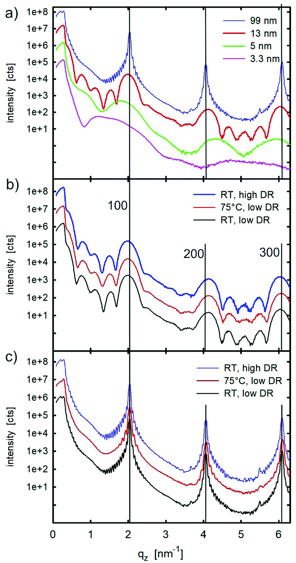 | ||
| Fig. 4 Specular X-ray reflectivity of (a) films with different thickness prepared at room temperature (RT) and a low deposition rate (0.15 nm min−1, low DR); and of films prepared at different conditions with a nominal thickness of (b) 13 nm and of (c) 99 nm. The intensity scales are given for the blue curves; all other curves are vertically shifted for clarity. | ||
 | ||
| Fig. 5 (a) X-ray reflectivity of a 5 nm thick film prepared at a substrate temperature of 75 °C and at a low deposition rate (0.15 nm min−1) with a fit to obtain the electron density profile perpendicular to the surface normal (z-direction), (b) electron density profile as obtained by the fit of the X-ray reflectivity curve and a direct comparison with results of the atomic force microscopy studies. | ||
The electron density profile from the XRR can be compared to the results from AFM. For this comparison the molecule has to be divided into segments with different electron densities: side chains are assumed to have a lower electron density than that of the aromatic core.34 The values used are 282 nm−3 and 520 nm−3 for the aliphatic chains and the aromatic core, respectively, their characteristic lengths are 0.9 nm and 1.2 nm, respectively. In addition, the coverage of the different monolayers has to be taken into account to obtain the final electron density profiles. Based on the AFM micrograph (Fig. S2, ESI†), we found a coverage of 94% for the first monolayer, 63% for the second monolayer, 6% and 2% for the third and fourth monolayer.
Based on this information, the expected electron density profile is plotted with vertical bars in Fig. 5b. The agreement between the fitted electron density from the XRR data and the calculated electron density from the AFM data is reasonably good so that the orientation of the molecules within the first monolayers can be determined. We find upright-standing molecules in a nearly closed first monolayer and in a partially covered second monolayer.
The X-ray reflectivity of the films with thicknesses of 13 and 99 nm (Fig. S4 and S5, ESI†) were fitted by assuming upright-standing molecules with modulation of the electron density according to the individual segments of the molecule (i.e. aromatic core and aliphatic chains). The fit of the experimental data is based on a stack of fully closed monolayers with a partially covered top layer. For the 13 nm film, five closed layers were used in the fit and, for the 99 nm film, 33 layers were required to obtain a good fit. In both cases, film thickness oscillations at low q-values (Kiessig fringes) as well as the coherent film thickness (Laue fringes) around the Bragg peaks could be clearly explained with the fits. Please note that the crystal size (coherent film thickness) agrees very well with the nominal film thickness. Detailed consideration of the XRR curve of the 99 nm thick sample (Fig. 4a) reveals two separated critical angles of total external reflection. The first, located at 0.163°, is related to the organic film, the second located at 0.218° is related to the silicon dioxide substrate. Their positions were determined by half of the intensity drops for the organic film and at half of the intensity maximum for the silicon dioxide substrate. Based on these values, the average electron densities can be determined; values of 378 nm−3 and 677 nm−3 are obtained for the two materials, respectively. The value for the organic material agrees very well with the average electron density from the different segments of the molecule used to fit the experimental data, the expected value derived from the known crystal structure of the SIP would be 371 nm−3. The observed electron density of the silicone dioxide substrate justifies the scaling of the electron density profile fits (Fig. 5b).
XRR curves from 13 nm thick films prepared under different sample preparation conditions are shown in Fig. 4b. There are no clear differences in the pattern, so that a similar morphology as well as crystalline structure can be assumed for 13 nm films with different preparation conditions. Also, the XRR curves of the 99 nm thick films prepared under different sample preparation conditions (Fig. 4c) are found to be similar to each other; however, there are some distinct differences. While the two patterns of the films which are prepared at room temperature (at low and high deposition rates) show identical features, the films prepared at an elevated substrate temperature are slightly different; the Laue fringes in the vicinity of the Bragg peaks are less pronounced and the Kiessig fringes close to the critical angles are missing. In this particular case, a lower uniformity across the thin film surface is present which accounts for the observed phenomena.
C Grazing incidence X-ray diffraction
The crystalline structure of the films was also probed by GIXD. Fig. 6 shows diffraction patterns of films with nominal thicknesses of 3 nm (one monolayer), 6 nm (a double layer) and 15 nm of a multilayer film. In the cases of the 6 nm and multilayer films, clear Bragg peaks are observed. In both cases calculated peak positions and peak intensities (calculated from their structure factors) are plotted based on the known structure of the substrate-induced phase of the molecule C8O-BTBT-OC8 with a 001 texture (i.e. the molecules are upright-standing on the substrate surface).22 The agreement between the measured data and the calculated peak positions and intensities is very good, so it can be concluded that this phase is present within the films presented here with a 100 orientation of the crystallites. In contrast, the diffraction pattern of the monolayer film (Fig. 6a) shows Bragg rods rather than the clear diffraction peaks which are observed for the thicker films. These rods reflect the two-dimensional order within the monolayer. The qxy position of the Bragg rods agrees quite well (within the experimental resolution) with the Bragg peak series in the thicker films. Along the Bragg rods, there is a progression in intensity: in the first rod (located at qxy = 13.3 nm−1) enhanced intensities are found at qz = 1 nm−1 and at qz = 3 nm−1, the second rod (located qxy = 16.2 nm−1) shows enhanced intensity at qz = 0.3 nm−1. These intensities reflect the alignment and conformation of the molecules within the first monolayer.35 The similarities in the diffraction patterns of the monolayer sample and the thicker films reveal that the molecular order and orientation within the first monolayer is comparable to the order within the substrate-induced phase structure of the molecule.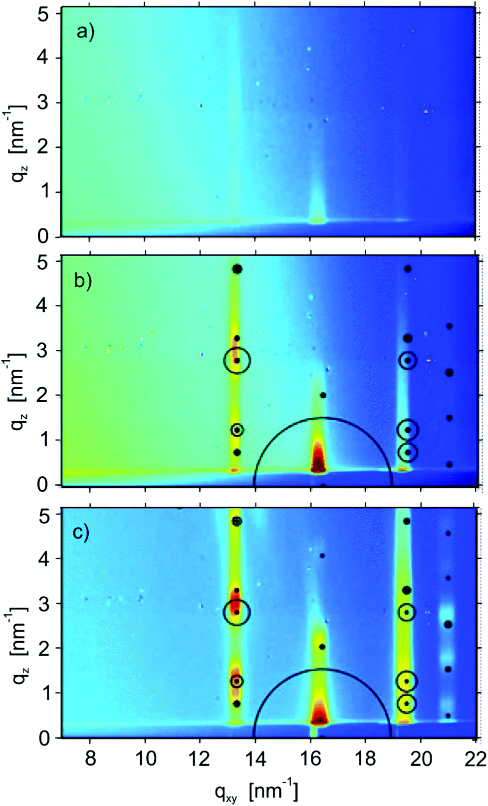 | ||
| Fig. 6 Grazing incidence X-ray diffraction data from films prepared at room temperature at low deposition rates (0.15 nm min−1) with nominal thicknesses of 3 nm/1 monolayer (a), of 6 nm/2 monolayers (b), and of a multilayer film (c). Calculated peak positions and their structure factors based on the known substrate-induced phase structure with a 001 orientation are shown by circles, where the size of the circle corresponds to calculated intensity. | ||
Discussion
The thin film growth of conjugated molecules on surfaces can follow different scenarios which are typically described by a roughening of the film surface with increasing film thickness. Amorphous films have a strong tendency to form smooth layers up to very thick films.36 However, in the case where the film crystallizes, the roughness typically increases considerably with the film thickness.37 In the case presented here, there is a crystalline film which shows the completion of the first monolayer before the onset of the second monolayer (compare Fig. 3a and e). A slight increase of the nominal film thickness to 1.6 monolayers already leads to a terrace-like structure with three terrace levels visible (Fig. 3b and f). This microscopic picture of film growth could also be confirmed by X-ray reflectivity investigations (Fig. 5). After the first few monolayers, the number of terrace levels at the film surface increases only slowly with the film thickness: about three terrace levels are observed for film thicknesses of 13 nm and four levels for the 99 nm thick film.In a next step, the evolution of the surface roughness is considered. Fig. 7 gives the surface roughness as a function of the film thickness in a double logarithmic representation; the values for the surface roughness are determined from the AFM images. Assuming an exponential relationship between the surface roughness (σRMS) and the nominal film thickness, a fit of the experimental data reveals a growth exponent β ∼ 0.1; the fit is given in Fig. 7 by a thick solid line. The value for the film with a thickness of 3.3 nm was not included into the fit, since the thin film growth mode is different for the formation of the first monolayer. For comparison, the random deposition limit with a growth exponent β = 1/2 is plotted in Fig. 7. This is expected for kinetic roughening assuming that the molecules do not diffuse across different terrace levels.38 Such cases have been experimentally observed;39,40 but also rapid surface roughening is frequently observed with growth exponents of β > 1/2.41,42 A growth exponent smaller than β = 1/2 reveals that diffusion across step edges is possible, however the detailed shape of the step edges play an important role for overcoming the barrier.9,43
 | ||
| Fig. 7 Root mean square surface roughness (σRMS) for thin films of the molecule C8O-BTBT-OC8 as a function of the film thickness. Values for films prepared at a low deposition rate (0.15 nm min−1) at room temperature (RT) and at 75 °C are shown. The thick solid line represents a fit of the experimental data by an exponential function to determine the growth exponent β, the thin line represents a random deposition mode with a growth exponent of β = 1/2. | ||
In our case, we can conclude that the surface of the terraces is formed by collective layers of alkyl chains, as confirmed by X-ray reflectivity fits (Fig. 5 and Fig. S3, ESI†) and the GIXD results (Fig. 6), while the AFM investigations reveal sharp step edges (Fig. 3). It has already been shown that step edges of flexible alkyl chains support the diffusion between the different terrace levels, as shown by a comparative study of pentacene and alkylperylene-tetracarboxylic diimides.44,45
The smooth film surface at large film thicknesses has clear effects on the XRR investigations of the 13 nm and 99 nm films: film thickness oscillations (Kiessig fringes) are observed close to the angle of total external reflection (Fig. 4b and c). Additionally, coherent crystal size oscillations around the Bragg peaks (Laue fringes) are present which highlight uniform crystallite thicknesses within the films. Since the film thickness is identical to the thickness of the crystallites, it can be concluded that the film is built by continuous crystals throughout the whole film thickness. The GIXD investigations reveal the presence of the substrate-induced phase already in the first monolayer, it can be concluded that the crystal growth starts at the first monolayer and continues up to the final film thickness of 99 nm.
Interestingly, no transfer from the substrate-induced phase to the bulk crystal structure appears at large film thicknesses. In the case of pentacene, a critical film thickness of the substrate induced phase is reported at 50 nm.46 The transfer to the bulk phase is mediated by the dendritic shape of the islands and by the large surface roughness of pentacene thin films. Structural defects within single layers due to the dendritic character of monolayer formation are present. In addition, molecular disorder at step edges of terrace levels may play an important role in the phase transition process.47,48 In the case presented here, the low surface roughness together with the layer-type crystallisation supports the continuous growth of the substrate-induced phase up to large film thicknesses.
Conclusions
In summary, we investigated the crystallographic structure and morphology of thin films of the molecule 2,7-dioctyloxy[1]benzothieno[3,2-b]benzothiophene (C8O-BTBT-OC8) grown on silicon oxide surfaces. The films were prepared by physical vapor deposition using different substrate temperatures (room temperature and 75 °C) and different deposition rates (0.15 nm min−1 and 1.2 nm min−1). The film thicknesses were varied from 1.5 nm (sub-monolayer regime) up to 99 nm (33 monolayers). Combining X-ray reflectivity and atomic force microscopy with grazing incidence X-ray diffraction data reveals that the molecules form layers of upright-standing molecules with a layer thickness of 3 nm; the upper surface of the layers is formed by the terminal alkyl chains of the molecule. Terraced islands are formed by stacking of the layers. These results reveal that the migration of molecules at the thin film surface happens predominantly at layers formed by alkyl chains. The low surface roughness at large film thicknesses reveals that the molecules have some ability to diffuse across step edges formed by the different terrace levels. Additionally, it is observed that the coherent thin film thickness (crystal size) agrees quite well with the deposited film thickness. A transition from the substrate-induced phase to the bulk crystal structure is not observed in films with a thickness of up to 99 nm.Conflicts of interest
There are no conflicts to declare.Acknowledgements
The authors thank Diamond Light Source for access to beamline I07 (proposal SI13569-1). The authors thank Alexander Hinderhofer, University Tübingen for valuable discussions. This work was supported by the Fonds de la Recherche Scientifique – FNRS and the Fonds voor Wetenschappelijk Onderzoek – Vlanderen (FWO) under EOS project no. 005018F and the Austrian Science Fund (FWF): [P25887], [I1788].Notes and references
- A. O. F. Jones, B. Chattopadhyay, Y. Geerts and R. Resel, Adv. Funct. Mater., 2016, 26, 2233 CrossRef CAS.
- H. Chung and Y. Diao, J. Mater. Chem. C, 2016, 4, 3915 RSC.
- R. Ruiz, D. Choudhary, B. Nickel, T. Toccoli, K. C. Chang, A. C. Mayer, P. Clancy, J. M. Blakely, R. L. Headrick, S. Iannotta and G. G. Malliaras, Chem. Mater., 2004, 16, 4497 CrossRef CAS.
- T. Hosokai, A. Hinderhofer, F. Bussolotti, K. Yonezawa, C. Lorch, A. Vorobiev, Y. Hasegawa, Y. Yamada, Y. Kubozoro, A. Gerlach, S. Kera, F. Schreiber and N. Ueno, J. Phys. Chem. C, 2015, 119, 29027 CrossRef CAS.
- C. Lorch, R. Banerjee, C. Frank, J. Dieterle, A. Hinderhofer, A. Gerlach and F. Schreiber, J. Phys. Chem. C, 2015, 119, 819 CrossRef CAS.
- C. Lercher, C. Rothel, O. M. Roscioni, Y. H. Geerts, Q. Shen, C. Teichert, R. Fischer, G. Leising, M. Sferrazza, G. Gbabode and R. Resel, Chem. Phys. Lett., 2015, 630, 12 CrossRef CAS PubMed.
- E. K. Burnett, J. Ly, M. R. Niazi, L. Zhang, S. R. Mc Cuskey, A. Amassian, D. Smilgies, S. C. B. Mannsfeld and A. L. Briseno, Adv. Mater. Interfaces, 2018, 5, 1701607 CrossRef.
- C. W. Miller, A. Sharoni, G. Liu, C. Colesniuc, B. Fruhberger and I. K. Schuller, Phys. Rev. B: Condens. Matter Mater. Phys., 2005, 72, 104113 CrossRef.
- G. Hlawacek and C. Teichert, J. Phys.: Condens. Matter, 2013, 25, 143202 CrossRef PubMed.
- A. Winkler, Surf. Sci., 2016, 652, 367 CrossRef CAS PubMed.
- M. Truger, O. M. Roscioni, C. Rothel, D. Kriegner, C. Simbrunner, R. Ahmed, E. D. Glowacki, J. Simbrunner, I. Salzmann, A. M. Coclite, A. O. F. Jones and R. Resel, Cryst. Growth Des., 2016, 16, 3647 CrossRef CAS PubMed.
- A. C. Durr, F. Schreiber, K. A. Ritley, V. Kruppa, J. Krug, H. Dosch and B. Struth, Phys. Rev. Lett., 2003, 90, 016104 CrossRef CAS PubMed.
- G. Hlawacek, F. S. Khokhar, R. van Gastel, B. Poelsema and C. Teichert, Nano Lett., 2011, 11, 333 CrossRef CAS PubMed.
- T. Nonaka, Y. Mori, N. Nagai, Y. Nakagawa, M. Saeda, T. Takahagi and A. Ishitani, Thin Solid Films, 1994, 239, 214 CrossRef CAS.
- M. Dohr, H. M. A. Ehmann, A. O. F. Jones, I. Salzmann, Q. Shen, C. Teichert, C. Ruzie, G. Schweicher, Y. H. Geerts and R. Resel, Soft Matter, 2017, 13, 2322 RSC.
- H. Iino, T. Usui and J. Hanna, Nat. Commun., 2015, 6, 6828 CrossRef CAS PubMed.
- B. Kosata, V. Kozmik, J. Svoboda, V. Novotna, P. Vanek and M. Glogarova, Liq. Cryst., 2003, 30, 603 CrossRef CAS.
- H. Iino and J. Hanna, Adv. Mater., 2011, 23, 1748 CrossRef CAS PubMed.
- S. Steudel, S. De Vusser, S. De Jonge, D. Janssen, S. Verlaak, J. Genoe and P. Heremans, Appl. Phys. Lett., 2004, 85, 4400 CrossRef CAS.
- J. Martin, M. Dyson, O. G. Reid, R. P. Li, A. Nogales, D. M. Smilgies, C. Silva, G. Rumbles, A. Amassian and N. Stingelin, Adv. Electron. Mater., 2018, 4, 1700308 CrossRef.
- A. O. F. Jones, Y. H. Geerts, J. Karpinska, A. R. Kennedy, R. Resel, C. Röthel, C. Ruzié, O. Werzer and M. Sferrazza, ACS Appl. Mater. Interfaces, 2015, 7, 1868 CrossRef CAS PubMed.
- N. Bedoya-Martínez, B. Schrode, A. O. F. Jones, T. Salzillo, C. Ruzié, N. Demitri, Y. H. Geerts, E. Venuti, R. G. Della Valle, E. Zojer and R. Resel, J. Phys. Chem. Lett., 2017, 8, 3690 CrossRef PubMed.
- C. Ruzié, J. Karpinska, A. Laurent, L. Sanguinet, S. Hunter, T. D. Anthopoulos, V. Lemaur, J. Cornil, A. R. Kennedy, O. Fenwick, P. Samorì, G. Schweicher, B. Chattopadhyay and Y. H. Geerts, J. Mater. Chem. C, 2016, 4, 4863 RSC.
- D. Nečas and P. Klapetek, Open Phys., 2012, 10, 181 Search PubMed.
- S. M. Danauskas, D. Li, M. Meron, B. Lin and K. Y. C. Lee, J. Appl. Crystallogr., 2008, 41, 1187 CrossRef CAS.
- C. Nicklin, T. Arnold, J. Rawle and A. Warne, J. Synchrotron Radiat., 2016, 23, 1245 CrossRef CAS PubMed.
- D. Kriegner, E. Wintersberger and J. Stangl, J. Appl. Crystallogr., 2013, 46, 1162 CrossRef CAS PubMed.
- A. Moser, PhD thesis, Graz University of Technology, Austria, 2012.
- L. Lyu, D. Niu, H. Xie, Y. Zhao, N. Cao, H. Zhang, Y. Zhang, P. Liu and Y. Gao, Phys. Chem. Chem. Phys., 2017, 19, 1669 RSC.
- T. Izawa, E. Miyazaki and K. Takimiya, Adv. Mater., 2008, 20, 3388 CrossRef CAS.
- B. Stadlober, U. Haas, H. Maresch and A. Hase, Phys. Rev. B: Condens. Matter Mater. Phys., 2006, 74, 165302 CrossRef.
- R. Matsubara, M. Sakai, K. Kudo, N. Yoshimoto, I. Hirosawa and M. Nakamura, Org. Electron., 2011, 12, 195 CrossRef CAS.
- A. Neuhold, H. Brandner, S. J. Ausserlechner, S. Lorbek, M. Neuschitzer, E. Zojer, C. Teichert and R. Resel, Org. Electron., 2013, 14, 479 CrossRef CAS PubMed.
- M. Dohr, O. Werzer, Q. Shen, I. Salzmann, C. Teichert, C. Ruzié, G. Schweicher, Y. H. Geerts, M. Sferrazza and R. Resel, ChemPhysChem, 2013, 14, 2554 CrossRef CAS PubMed.
- V. M. Kaganer, H. Mohwald and P. Dutta, Rev. Mod. Phys., 1999, 71, 779 CrossRef CAS.
- L. F. Cheng, L. S. Liao, W. Y. Lai, X. H. Sun, N. B. Wong, C. S. Lee and S. T. Lee, Chem. Phys. Lett., 2000, 319, 418 CrossRef CAS.
- S. Kowarik, A. Gerlach, S. Sellner, F. Schreiber, J. Pflaum, L. Cavalcanti and O. Konovalov, Phys. Chem. Chem. Phys., 2006, 8, 1834 RSC.
- T. Michely and J. Krug, Islands Mounds and Atoms, Springer Series in Surface Sciences, Berlin, 2004, vol. 42 Search PubMed.
- A. R. Woll, T. V. Desai and J. R. Engstrom, Phys. Rev. B: Condens. Matter Mater. Phys., 2011, 84, 075479 CrossRef.
- G. X. Zhang, B. L. Weeks and M. Holtz, Surf. Sci., 2011, 605, 463 CrossRef CAS.
- S. D. Wang, X. Dong and C. S. Lee, J. Phys. Chem. B, 2005, 109, 9892 CrossRef CAS PubMed.
- F. Biscarini, P. Samori, O. Greco and R. Zamboni, Phys. Rev. Lett., 1997, 78, 2389 CrossRef CAS.
- J. E. Goose, E. L. First and P. Clancy, Phys. Rev. B: Condens. Matter Mater. Phys., 2010, 81, 205310 CrossRef.
- E. R. Kish, R. K. Nahm, A. R. Woll and J. R. Engstrom, J. Phys. Chem. C, 2016, 120, 6165 CrossRef CAS.
- A. Zykov, S. Bommel, C. Wolf, L. Pithan, C. Weber, P. Beyer, G. Santoro, J. P. Rabe and S. Kowarik, J. Chem. Phys., 2017, 146, 052803 CrossRef PubMed.
- T. Kakudate and N. Yoshimoto, Appl. Phys. Lett., 2007, 90, 81903 CrossRef.
- S. Pachmajer, A. O. F. Jones, M. Truger, C. Rothel, I. Salzmann, O. Werzer and R. Resel, ACS Appl. Mater. Interfaces, 2017, 9, 11977 CrossRef CAS PubMed.
- C. Westermeier, A. Cernescu, S. Amarie, C. Liewald, F. Keilmann and B. Nickel, Nat. Commun., 2014, 5, 4101 CrossRef CAS PubMed.
Footnote |
| † Electronic supplementary information (ESI) available. See DOI: 10.1039/c9tc01979k |
| This journal is © The Royal Society of Chemistry 2019 |