
Electronic structure engineering of tin telluride through co-doping of bismuth and indium for high performance thermoelectrics: a synergistic effect leading to a record high room temperature ZT in tin telluride†
U. Sandhya
Shenoy
 *a and
D. Krishna
Bhat
*b
*a and
D. Krishna
Bhat
*b
aDepartment of Chemistry, College of Engineering and Technology, Srinivas University, Mukka, Mangalore-574146, India. E-mail: sandhyashenoy347@gmail.com
bDepartment of Chemistry, National Institute of Technology Karnataka, Surathkal, Mangalore-575025, India. E-mail: denthajekb@gmail.com
First published on 23rd March 2019
Abstract
The ever increasing demand for alternative clean energy sources has led to intense research towards the optimization of thermoelectric performance of known systems. In this work, we engineer the electronic structure of SnTe by co-doping it with Bi and In. The co-doping not only results in the formation of two different resonance states and a reduced valence band offset, as in the case of previously reported co-doped SnTe, but also leads to opening of the band gap, which otherwise was closed in the case of Bi and In doped SnTe configurations, leading to suppression of bipolar diffusion. The synergistic action of all these effects leads to an increased Seebeck co-efficient throughout the temperature range and a ZTmax of ∼1.32 at 840 K. This strategy of co-doping two different resonant dopants resulted in a record high room temperature ZT of ∼0.25 at 300 K for SnTe based materials. This work suggests that appropriate combination of dopants to engineer the electronic structure of a material can lead to unpredictable results.
1. Introduction
Thermoelectric (TE) materials with the potential to convert waste heat into electricity have made a name in clean energy sources.1–3 Metal chalcogenides, particularly lead-free SnTe, have been recently sought after for resolving the world-wide energy crisis due to their tunable TE properties.1,2,4 The dimensionless figure of merit, ZT, which is given by ZT = σS2T/κ, where σ is electrical conductivity, S is the Seebeck co-efficient and κ is total thermal conductivity, governs the TE efficiency of a material. The conflicting nature of the terms involved makes optimization of ZT a tricky problem. Hence, there is an urgent need to develop strategies to either come up with new materials with intriguing properties or improve the properties of the existing TE materials.5–7Although SnTe on its own has a very small value for ZT, various strategies have been implemented in the past to improve its efficiency for application as a TE material.1 Doping and co-doping of various elements for carrier concentration optimization, electronic structure engineering and nanostructuring have been implemented to improve the power factor as well as to decrease the total thermal conductivity of the material.2 Co-doping of SnTe with Ag–In, Ca–In, Cd–In, Hg–In, Mg–In, and Mn–In has been particularly useful as it is able to simultaneously introduce a resonance level as well as decrease the energy difference between valence sub-bands, which synergistically leads to an enlarged ZT of about ∼1.65 at 840 K in the case of Ca–In co-doped SnTe, which is by far the maximum value in the case of SnTe based materials.8–14 Although in the above mentioned cases doping of M (M = Ag, Ca, Cd, Hg, Mg, and Mn) individually in SnTe enlarges the band gap, co-doping of M and In generally decreases or completely closes the band gap. However, it may be noted here that the effect of co-doping two resonant dopants has not been reported.
Bi doping in SnTe is known to modulate the carrier concentration of SnTe and enhance the S values while In is known to introduce a resonance level and thereby improve the S values.15,16 Herein, we study co-doping of Bi and In in SnTe and its effect on the TE properties both theoretically and experimentally. The effect of co-doping Bi–In in SnTe on the electronic structure was studied using first principles density functional theory (DFT) simulations. Bi–In co-doped SnTe was prepared through sealed tube melting reactions keeping the ratio of Bi to In as 2![[thin space (1/6-em)]](https://www.rsc.org/images/entities/char_2009.gif) :1 (see the ESI† for details on methods).
:1 (see the ESI† for details on methods).
2. Results and discussion
The first principles DFT calculations of the electronic structure of a 2 × 2 × 1 supercell of SnTe revealed a direct band gap of 0.081 eV with conduction and valence band edges symmetric through the gap at the Z point and an energy difference of 0.263 eV between the light hole (at the Z point) and the heavy hole (at the M + δ point along the M → Γ direction) valence sub-bands (Fig. 1a). The valence band is primarily constituted by Te ‘p’ orbitals while the conduction bands have a predominant Sn ‘p’ character (Fig. S1, ESI†). Fig. 1b shows the electronic structure of Sn15InTe16 wherein the valence band maximum (VBM) splits off as resonance levels and shuts down the band gap, as well documented in the previous literature.8,9 The appearance of a hump within the valence band in the density of state (DOS) plot due to the In ‘s’ orbital confirms the presence of the resonance level (Fig. S2, ESI†).10 The hybridization between the In ‘s’ orbital and Te ‘p’ orbitals in the ‘deep defect states’ appearing at the Fermi level around ∼0 eV and ‘hyperdeep defect states’ appearing around ∼−5.5 eV can be clearly seen in Fig. S1 and S2 (ESI†) showing the dramatic change in the appearance of the Te ‘p’ orbitals in the presence of In. The electronic structure of Sn15BiTe16 reveals that doping of Bi in SnTe disturbs the degeneracy of the conduction band minimum (CBM) and the impurity induced band appears as resonance states and closes the band gap at the Z point (Fig. 1c). This observation of shutting down the band gap agrees very well with the previously reported Bi doped SnTe.17 The impurity induced band appears as a hump below the CBM in the DOS plot due to the contribution from the Bi ‘p’ orbitals (Fig. S2, ESI†). We see that the Fermi level lies in the conduction band, making it an n-type material.17 This nature of Bi impurity induced resonance states is seen in the case of PbTe also.18 We see that in SnTe, the resonance states introduced by ‘p’ valence electron impurities are rather broader than that of the ‘s’ valence electron impurities, as in the case of PbTe.18 When Bi and In are simultaneously co-doped in SnTe, we see an unexpected change in the electronic structure. The electronic structure of Sn14BiInTe16 shows the presence of resonance levels due to both Bi and In (Fig. 1d). It also reveals that the initially eight fold degenerate band (due to spin orbit coupling) of SnTe splits into four two-fold degenerate bands due to the co-doping of In and Bi. Prominent humps are seen in the DOS plot, which could be matched with the contribution from the In ‘s’ orbital for the resonance states closer to the VBM and that from the Bi ‘p’ states for the resonance level near the CBM (Fig. S3, ESI†). Here also we see contributions from the Te ‘p’ orbitals to the localized bands due to the hybridization as in the individual doping cases (Fig. S1, ESI†). The interesting feature to be noted here is that although both Bi and In when individually doped close the band gap of SnTe, when co-doped, the principal band gap at the Z point increases to 0.096 eV. In previously reported Ag–In and Ca–In co-doped SnTe, the principal band gap, which is enlarged due to Ag/Ca doping, shuts down when co-doped with In.8,9 Although there is a large increase in the band gap due to doping of Cd/Mn in SnTe, co-doping it along with In resulted in the decrease of the band gap.10,14 Previously, when Ag was co-doped along with Bi in SnTe, there also we saw that the impurity induced band due to Bi got pulled down so much lower that it resulted in a larger overlap with the valence band despite Ag having the ability to increase the band gap.17 To the best of our knowledge, this is the first case where we see that co-doping of Bi and In enlarges the band gap in the co-doped configuration. When co-doping of Bi and In is done in a 2:1 ratio, viz. Sn13Bi2InTe16, we see that the band gap further enlarges to 0.2 eV (Fig. 2). This shows that the right combination of co-dopants is essential in order to enlarge the band gap since a larger band gap is very much essential to counteract the detrimental effect of bipolar diffusion on the Seebeck as well as thermal conductivity values. When the ratio of Bi and In is changed from 1:1 to 2:1, we see that the edges of light and heavy hole valence sub-bands approach each other further with the energy difference decreasing to 0.068 eV for the 2:1 configuration from the calculated value of 0.145 eV for the 1:1 configuration. Due to the above said facts, the 2:1 ratio for co-doping was maintained during the synthesis of samples.
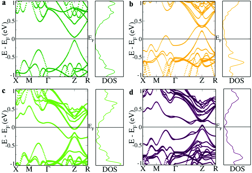 | ||
| Fig. 1 Electronic structure and DOS of (a) Sn16Te16, (b) Sn15InTe16, (c) Sn15BiTe16, and (d) Sn14BiInTe16. The principal band gap occurring at the L point folds onto the Z point and the heavy hole valence band occurring at the Σ point folds on the M + δ point along the M → Γ direction due to the dimensions of the supercell (2 × 2 × 1) used. The resonant states can clearly be identified in the form of humps in the respective DOS for the doped and co-doped configurations. | ||
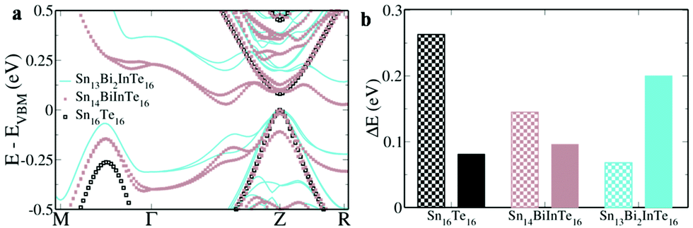 | ||
| Fig. 2 Comparison of (a) electronic structures and (b) band gaps (solid bars) and energy differences between light and heavy hole valence subbands (checkered bars) of Sn16Te16, Sn14BiInTe16 and Sn13Bi2InTe16. The increase in the band gap and the decrease in the energy offset of valence subbands are clearly seen in the electronic structure as the Bi–In ratio changes from 1:1 to 2:1. In the electronic structure, the energies are shifted with respect to the energy of the valence band maximum (VBM), which is set at zero. | ||
Fig. 3a reveals the powder X-ray diffraction pattern of Sn1−3xBi2xInxTe (x = 0.00 to 0.03), which could be indexed to the face centered cubic structure of sodium chloride (space group Fm3m). For the x = 0.03 composition, deviation from a single phase is observed as we see extra peaks appearing that could be indexed to a Bi precipitate. Since the ionic radius of Bi3+ is higher than Sn2+ by 0.03 Å and that of In is comparable to Sn, we see a linear increase in the lattice parameter for the co-doped compositions (Fig. 3b).9 The TEM images reveal that for the x = 0.03 composition, Bi precipitates (around 2–10 nm in size) start appearing that are absent at lower concentrations of doping (Fig. 3c, d and Fig. S4, ESI†). The elemental composition for various spots encircled in the TEM image, obtained via energy dispersive spectrometry (EDS), is given in Table S1 (ESI†).
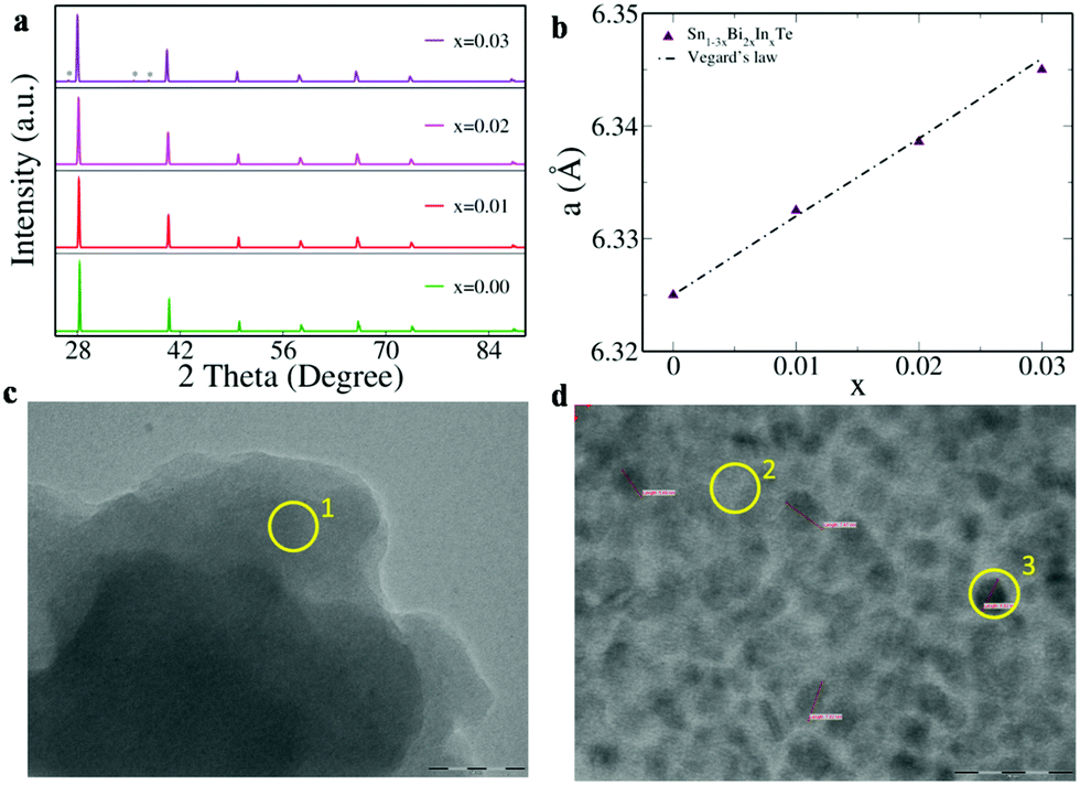 | ||
| Fig. 3 (a) Powder XRD pattern; * in the uppermost panel indicates peaks due to Bi precipitates. (b) Variation of lattice parameter ‘a’ of Sn1−3xBi2xInxTe versus dopant concentration ‘x’. TEM images of (c) Sn0.94Bi0.04In0.02Te and (d) Sn0.91Bi0.06In0.03Te showing nanoparticle formation when x = 0.03. The scale in ‘c’ measures 50 nm and in ‘d’ measures 20 nm. The percentage elemental composition of the area marked in the yellow circle is given in Table S1 (ESI†). | ||
Electrical conductivity values of Sn1−3xBi2xInxTe as a function of temperature and doping concentration were observed to decrease (Fig. 4a). The decrease with respect to the increase in the temperature is due to the degenerate semiconducting nature while the decrease in value with an increase in the dopant concentration is due to the decrease in the carrier concentration from 4.1 × 1020 cm−3 (x = 0.00) to 2.9 × 1020 cm−3 (x = 0.03). The formation of resonance states by both Bi and In, opening of the band gap and approaching of the valence sub-band edges towards each other as revealed by the DFT calculations have a profound impact on the Seebeck co-efficient values (Fig. 4b). The room temperature values of S increase from 36 μV K−1 (x = 0.00) to 107 μV K−1 (x = 0.03) and a maximum of 198 μV K−1 at 840 K is reached for x = 0.03. Comparison of the room temperature values of S with the Pisarenko plot reported by Zhang et al. (Fig. S5, ESI†) reveals that the S value for pristine SnTe falls exactly on top of the line while those of the co-doped samples are much higher than the predicted values.16 This is attributed to the increase in band effective mass due to the resonant states introduced by both Bi and In. Also, the decrease in the separation of light and heavy hole valence bands as determined by the DFT study increases the valley degeneracy from 4 to 16 (4 from light and 12 from heavy hole bands) and hence increases the Seebeck values.12 The effect of dopants on the Seebeck values was also determined theoretically using the Boltztrap code.19 The variation of calculated Seebeck coefficient as a function of chemical potential (μ) in the temperature range of 300–800 K is shown in Fig. S6 (ESI†). The negative and positive chemical potentials indicate the hole and electron doping corresponding to p and n-type doping, respectively. At a particular value of μ, the value of S increases with an increase in temperature. The positive Seebeck peak is found in the negative chemical potential region in Bi doped SnTe due to the Fermi level lying almost at the tip of the conduction band with a resonant peak lying below the Fermi level (Fig. S6a, ESI†). In the case of In doped SnTe, the positive Seebeck peak lies in the positive chemical potential region because of the presence of the Fermi level in the valence band and the resonance level appearing above the Fermi level (Fig. S6b, ESI†). This indicates that the resonance states are responsible for the increase in the S values in both cases. The Seebeck peak lies in the positive potential range closer to the Fermi level due to the Fermi level residing at the top of the valence band, as revealed in the electronic structure (Fig. S6c, ESI†). The features of both singly doped configurations are present in the co-doped configuration. The co-doped SnTe configuration exhibits a higher Seebeck coefficient at larger potential windows at higher temperatures. These results suggest that ZT can be improved for a wide range of carrier concentrations at higher temperatures. Further, this observation also indirectly supports the fact that bipolar diffusion is prevented due to the larger band gap of the co-doped sample.
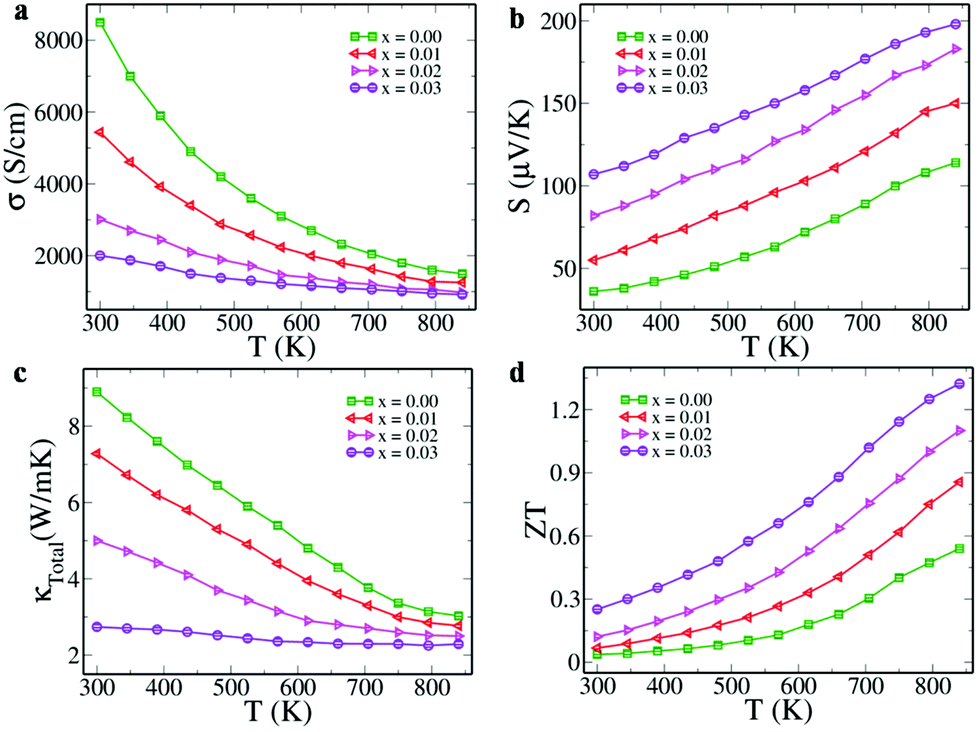 | ||
| Fig. 4 Variation of (a) electrical conductivity, (b) Seebeck coefficient, (c) thermal conductivity, and (d) ZT with temperature in Sn1−3xBi2xInxTe. The positive value of the Seebeck coefficient reveals that holes are the majority carriers leading to p-type conduction in the material. | ||
A maximum power factor (given by σS2) of ∼36 μW cm−1 K−2 was observed when x = 0.03 at 840 K (Fig. S7, ESI†), which is appreciably higher than the optimized compositions of Bi doped SnTe (∼20 μW cm−1 K−2) and In doped SnTe (∼21 μW cm−1 K−2) reported previously.15,16 Although the electrical conductivity decreases with increasing temperature, the large increase in S value makes the power factor increase as a function of temperature and dopant fraction. The total thermal conductivity of the samples decreases as a function of temperature and dopant concentration (Fig. 4c). The lattice thermal conductivity was obtained by subtracting the electronic thermal conductivity from the total thermal conductivity. The lattice thermal conductivity shows a decreasing trend with increasing temperature and dopant concentration (Fig. S8, ESI†). This indicates that the dopants effectively scatter the heat carrying phonons due to mass contrast. Moreover, the formed Bi nanoprecipitates in the Sn1−3xBi2xInxTe (x = 0.03) sample further scatter the additional phonons causing the decrease in the thermal conductivity values.5 Also, the increase in the band gap of the material, as revealed by DFT studies, prevents the bipolar thermal transport from further decreasing the total thermal conductivity.
We see that the ZT value increases both as a function of temperature and dopant concentration (Fig. 4d). We report here a record high room temperature ZT of ∼0.25 at 300 K, higher than the previously reported record high value of ∼0.2 for Ca doped SnTe.20 The result of all these thermal transport properties is the ZTmax value of ∼1.32 attained at 840 K for x = 0.03 and ZTavg of ∼0.73, considering 300 and 840 K as cold and hot ends, respectively. These values are comparable to the ZTmax value of ∼1.4 at 923 K and ZTavg of ∼0.78 between 300 and 900 K reported for Cd–In co-doped SnTe. Our reported ZTmax is also comparable to the value of ∼1.4 (at 773 K) recently reported for In–I co-doped PbTe. Notably, our material has the advantage of being free from toxic Cd and Pb and is hence more environmentally benign.10,21 The reported ZTmax value is higher than the previously reported values for SnTe singly doped with In (∼1.1 at 873 K) and Bi (∼1.1 at 873 K), and co-doped with Ag–In (∼1 at 856 K), Cd–In (∼1.1 at 850 K), Hg–In (∼0.9 at 850 K), and Mn-In (∼1.03 at 923 K), and Sn1−xPbxTe (x = 0.3) co-doped with Mg–In (∼1 at 710 K).8,11,13–16,22 The ZT values of the Bi–In co-doped SnTe are found to be much higher than the Bi/In singly doped SnTe, as revealed in Fig. S9 (ESI†), indicating the synergistic effect of the dopants. Although the reported value of ZTmax in the present work is lower than the one reported for Ca–In co-doped SnTe (∼1.65 at 840 K), which by far holds the record in SnTe based materials, the ZTavg value reported here is ∼0.95, much higher than ∼0.87 reported for Ca–In co-doped SnTe for the same temperature range of 500–840 K, indicating its higher potential for thermoelectric application, as the efficiency of a TE device depends more on ZTavg than ZTmax.9
3. Conclusions
In this work, we engineer the electronic structure of SnTe by co-doping it with Bi and In using first principles DFT simulations and experiments. For the first time, we report that Bi introduces resonance states in SnTe. We see that the co-doping of two different resonant dopants not only results in edges of valence sub-bands approaching one another but also leads to opening of the band gap, which otherwise was closed in the case of the doped Bi and In configurations. This leads to an increased Seebeck co-efficient throughout the temperature range and reduced thermal conductivity at elevated temperatures due to the suppression of the bipolar diffusion and the formation of nanoprecipitates at x = 0.03 in Sn1−3xBi2xInxTe. The synergistic action of all these effects makes the material achieve a record high room temperature ZT of ∼0.25 at 300 K for SnTe based materials and a maximum ZT of ∼1.32 at 840 K, making it a promising thermoelectric material. This strategy of co-doping n-type and p-type resonant dopants to increase the band gap of SnTe and to introduce deep defect states to improve ZT throughout the temperature range can potentially be used for other materials as well.Conflicts of interest
There are no conflicts of interest to declare.Acknowledgements
The authors gratefully acknowledge the financial support received from the SERB, Govt. of India and the CSIR, Govt. of India in the form of R&D project grants and the DST for the INSPIRE Faculty award.References
- S. Li, X. Li, Z. Ren and Q. Zhang, Recent progress towards high performance of tin chalcogenide thermoelectric materials, J. Mater. Chem. A, 2018, 6, 2432–2448 RSC.
- R. Moshwan, L. Yang, J. Zou and Z. G. Chen, Eco-friendly SnTe thermoelectric materials: progress and future challenges, Adv. Funct. Mater., 2017, 27, 1703278 CrossRef.
- Y. Liu, W. Wang, J. Yang and S. Li, Recent advances of layered thermoelectric materials, Adv. Sustainable Syst., 2018, 2, 1800046 CrossRef.
- P. Ren, Y. Liu, J. He, T. Lv, J. Gao and G. Xu, Recent advances in inorganic material thermoelectrics, Inorg. Chem. Front., 2018, 5, 2380–2398 RSC.
- X. Zhou, Y. Yan, X. Lu, H. Zhu, X. Han, G. Chen and Z. Ren, Routes for high-performance thermoelectric materials, Mater. Today, 2018, 21, 974–988 CrossRef CAS.
- S. U. Shenoy and D. K. Bhat, Enhanced bulk thermoelectric performance of Pb0.6Sn0.4Te: effect of magnesium doping, J. Phys. Chem. C, 2017, 121, 20696–20703 CrossRef CAS.
- A. Banik, U. S. Shenoy, S. Anand, U. V. Waghmare and K. Biswas, Mg Alloying in SnTe Facilitates Valence Band Convergence and Optimizes Thermoelectric Properties, Chem. Mater., 2015, 27, 581–587 CrossRef CAS.
- A. Banik, U. S. Shenoy, S. Saha, U. V. Waghmare and K. Biswas, High Power Factor and Enhanced Thermoelectric Performance of SnTe-AgInTe2: Synergistic Effect of Resonance Level and Valence Band Convergence, J. Am. Chem. Soc., 2016, 138, 13068–13075 CrossRef CAS PubMed.
- D. K. Bhat and S. U. Shenoy, Enhanced thermoelectric performance of bulk tin telluride: synergistic effect of calcium and indium co-doping, Mater. Today Phys., 2018, 4, 12–18 CrossRef.
- G. Tan, F. Shi, S. Hao, H. Chi, L. D. Zhao, C. Uher, C. Wolverton, V. P. Dravid and M. G. Kanatzidis, Codoping in SnTe: Enhancement of Thermoelectric Performance through Synergy of Resonance Levels and Band Convergence, J. Am. Chem. Soc., 2015, 137, 5100–5112 CrossRef CAS PubMed.
- X. Tan, X. Tan, G. Liu, J. Xu, H. Shao, H. Hu, M. Jin, H. Jiang and J. Jiang, Optimizing the thermoelectric performance of In-Cd codoped SnTe by introducing Sn vacancy, J. Mater. Chem. C, 2017, 5, 7504–7509 RSC.
- D. K. Bhat and S. U. Shenoy, High thermoelectric performance of co-doped tin telluride due to synergistic effect of magnesium and indium, J. Phys. Chem. C, 2017, 121, 7123–7130 CrossRef CAS.
- X. Tan, G. Liu, J. Xu, X. Tan, H. Shao, H. Hu, H. Jiang, Y. Lu and J. Jiang, Thermoelectric properties of In–Hg co-doping in SnTe: energy band engineering, J. Materiomics, 2018, 4, 62–67 CrossRef.
- H. Wang, J. Hwang, C. Zhang, T. Wang, W. Su, H. Kim, J. Kim, J. Zhai, X. Wang, H. Park, W. Kim and C. Wang, Enhancement of the thermoelectric performances of bulk SnTe alloys via the synergistic effect of band structure modification and chemical bond softening, J. Mater. Chem. A, 2017, 5, 14165–14173 RSC.
- Z. Zhou, J. Yang, Q. Jiang, Y. Luo, D. Zhang, Y. Ren, X. He and J. Xin, Multiple effects of Bi doping in enhancing the thermoelectric properties of SnTe, J. Mater. Chem. A, 2016, 4, 13171–13175 RSC.
- Q. Zhang, B. Liao, Y. Lan, K. Lucas, W. Liu, K. Esfarjani, C. Opeil, D. Broido, G. Chen and Z. Ren, High Thermoelectric Performance by Resonant Dopant Indium in Nanostructured SnTe, Proc. Natl. Acad. Sci. U. S. A., 2013, 110, 13261–13266 CrossRef CAS PubMed.
- K. Hoang, S. D. Mahanti and M. G. Kanatzidis, Impurity clustering and impurity-induced bands in PbTe-, SnTe- and GeTe-based bulk thermoelectrics, Phys. Rev. B: Condens. Matter Mater. Phys., 2010, 81, 115106 CrossRef.
- S. Ahmad, S. D. Mahanti, K. Hoang and M. G. Kanatzidis, Ab initio studies of the electronic structure of defects in PbTe, Phys. Rev. B: Condens. Matter Mater. Phys., 2006, 74, 155205 CrossRef.
- G. K. H. Madsen and D. J. Singh, BoltzTrap. A code for calculating band structure dependent quantities, Comput. Phys. Commun., 2006, 175, 67–71 CrossRef CAS.
- R. A. R. A. Orabi, N. A. Mecholsky, J. Hwang, W. Kim, J. S. Rhyee, D. Wee and M. Fornari, Band Degeneracy, Low Thermal Conductivity, and High Thermoelectric Figure of Merit in SnTe-CaTe Alloys, Chem. Mater., 2016, 28, 376–384 CrossRef.
- Q. Zhang, Q. Song, X. Wang, J. Sun, Q. Zhu, K. Dahal, X. Lin, F. Cao, J. Zhou, S. Chen, G. Chen, J. Mao and Z. Ren, Deep defect level engineering: a strategy of optimizing the carrier concentration for high thermoelectric performance, Energy Environ. Sci., 2018, 11, 933–940 RSC.
- S. Roychowdhury, U. S. Shenoy, U. V. Waghmare and K. Biswas, An enhanced seebeck coefficient and high thermoelectric performance in p-type In and Mg co-doped Sn1−xPbxTe via the co-adjuvant effect of the resonance level and heavy hole valence band, J. Mater. Chem. C, 2017, 5, 5737–5748 RSC.
Footnote |
| † Electronic supplementary information (ESI) available: Methods, partial density of states showing contributions of various orbitals, TEM images, elemental composition from EDS results, the Pisarenko plot, variation of theoretically calculated Seebeck coefficient with chemical potential, and variation of power factor, lattice thermal conductivity and ZT with temperature. See DOI: 10.1039/c9tc01184f |
| This journal is © The Royal Society of Chemistry 2019 |