
 Open Access Article
 This Open Access Article is licensed under a Creative Commons Attribution-Non Commercial 3.0 Unported Licence
Multifunctional nanopatterned porous bismuth ferrite thin films
Alichandra
Castro
a,
Manuel A.
Martins
 b,
Liliana P.
Ferreira
cd,
Margarida
Godinho
c,
Paula M.
Vilarinho
*a and
Paula
Ferreira
*a
b,
Liliana P.
Ferreira
cd,
Margarida
Godinho
c,
Paula M.
Vilarinho
*a and
Paula
Ferreira
*a
aCICECO – Aveiro Institute of Materials, Department of Materials and Ceramics Engineering, University of Aveiro, 3810-193 Aveiro, Portugal. E-mail: paula.vilarinho@ua.pt; pcferreira@ua.pt; Fax: +351 234401470; Tel: +351 234401419
bCICECO – Aveiro Institute of Materials, Department of Physics, University of Aveiro, 3810-193 Aveiro, Portugal
cDepartment of Physics, University of Coimbra, 3004-516 Coimbra, Portugal
dBiosystems and Integrative Sciences Institute (BioISI), Faculdade de Ciências, University of Lisbon, 1749-016 Lisbon, Portugal
First published on 6th June 2019
Abstract
Nanopatterned porous thin films of bismuth ferrite (BiFeO3) with porosity perpendicular to the plane are prepared by an evaporation-induced self-assembly methodology using nitrate metal salts and a commercial block copolymer as a structure-directing agent. The sol–gel based method is successfully used to achieve crystalline nanopatterned porous BiFeO3 layers with 66 nm thickness and an average pore diameter of 100 nm after treatment at 600 °C. The large vertical porosity markedly enhances the nanoscale electric properties when compared to the dense counterparts. The porosity orients the piezoelectric domains and reduces the energy necessary to reorient the dipoles. The induced instability in the dipole–dipole interactions results in an increase of the effective piezoelectric coefficient. The porous structure also has a positive effect on the magnetic characteristics of the system, displaying a larger ferromagnetic component relative to the dense thin film counterparts. Thus, the vertical nanoporosity may have a broad impact in applications of ferroelectric and multiferroic thin films. Moreover, the nanoporosity may be used for further functionalization, aiming at the improvement of the weak ferromagnetic properties of BiFeO3 at room temperature and the enhancement of the magnetoelectric coupling. We may add that the nanoporosity is important for photocatalytic applications conjugating a low direct band gap (2.58 eV) and an extended porous area (ca. 57%), as well. Our observations though related to BiFeO3 can be extended to other ferroic systems and have a marked effect on the extended use of ferroic thin films with optimized properties for actuator, sensor and memory applications.
1. Introduction
BiFeO3 has been one of the most studied ferroic materials in the last few decades. BiFeO3, with a rhombohedral distorted perovskite structure, is a multiferroic material presenting the coexistence of large spontaneous electrical polarization and magnetization and coupling between these functionalities.1–3 The coexistence of ferroelectricity, ferroelasticity and antiferromagnetism below the Néel temperature makes this material particularly interesting for several applications, including multifunctional sensors, resistive memories, information storage, and spintronics, among others. In 2013, heteroepitaxially constrained BiFeO3 thin films presenting a substantial magnetization (∼150 emu cm−3) and enhanced ferroelectric polarization (50 to 60 μC cm−2) comparable to that of lead-based materials were reported.2 Beyond these attractive ferroic properties, BiFeO3 also presents interesting optical properties and, consequently a great potential for applications in solid state devices that utilize heterojunction effects, and in photovoltaic and photocatalytic devices due to its small bandgap.4–10Among the most common processing methods to prepare ferroic thin films and nanostructures, chemical solution deposition as sol–gel is a low cost method that offers high versatility for the synthesis and development of a wide range of compositions, nanostructures and properties.11 To fulfill the constant needs of the microelectronics industry of size and cost reduction, while enhancing performance, films with thickness below 100 nm and a well-patterned surface area are needed. The design of nanofeatures, uniform in size and shape at a reasonable large-scale/range order, i.e. “nanopatterning”, would extend the thin films’ utility for electronic devices and integrated circuits, which require that each pixel feature can be individually addressed. To the best of our knowledge, up to now, nanopatterned porous structures involving BiFeO3 were mainly produced by nanolithography based on the combination of the templated self-assembly method with electron-beam lithography (also named as soft electron-beam lithography),12–14 focused ion-beam15 or UV photolithography.16 Although, these thin films present well-defined structures, the application of such methods is limited by the high cost of the fabrication equipment and the difficulty to cover large surface areas. Moreover, the etching methods usually associated with lithography are typically harmful to the electric and magnetic properties of ferroics.
In recent years, we have been interested in nanostructuring multimetallic oxide ferroelectric porous phases by low cost solution-based methods. We have reported the preparation and characterization of porous ferroelectric thin films with around 100 nm thickness and with ∼50 nm pore size. We have proved the piezo- and ferro-electric properties at the nanoscale of porous barium titanate (BaTiO3) and lead titanate (PbTiO3) thin films.17,18 The main difficulty in this work is the control of the porosity order during the thermal treatment needed to crystalize the tetragonal phase. We have also observed that porosity induces the crystallization of tetragonal PbTiO3 at a temperature lower than that of the dense counterparts. Moreover for the same thermal conditions, the porous PbTiO3 films exhibit enhanced piezoelectric coefficients, switchable polarization and low local coercivity.17,18 In 2011, Brezesinski et al.19 reported the preparation of BiFeO3 thin films with anisotropic crystallites combined with a continuous mesoporosity using the same soft-templating methodology. However, these thin films do not present a porosity directed to the substrate. In addition, only the photocatalytic activity was studied. Quickel et al.20 reported the fabrication of porous BiFeO3 thin films by a similar methodology to that of Brezesinski et al.19 The films display order when amorphous, losing the organization upon crystallization. Recently, Zhang et al.21 identified in a review paper the opportunity of exploring texture and domain engineering in high quality BiFeO3 films using sol–gel methodology.
The present study aims to describe the preparation of a nanostructured porous thin film of BiFeO3 with highly uniform porosity perpendicular to the substrate surface, with ca. 66 nm thickness and an average pore size of 100 nm. This work also addresses the electrical and magnetic properties of the nanopatterned porous BiFeO3 thin films, not reported up to now. To understand the porosity effect on the material's ferroic response, a comparison with the bulk counterparts is established. Optical absorption behavior was also analyzed to exploit the multifunctional character of the nanopatterned porous BiFeO3 thin films and their potential for a wide range of applications.
2. Experimental
2.1 Film preparation
Nanopatterned porous BiFeO3 thin films were prepared using a sol–gel method and evaporation-induced self-assembly methodology. PB51-b-PEO62 block-copolymer with MWPB = 51![[thin space (1/6-em)]](https://www.rsc.org/images/entities/char_2009.gif) 000 g mol−1, MWPEO = 62000 g mol−1, from Polymer Source, was used as a structure-directing agent. Two solutions, solutions A and B, were prepared. In solution A, PB51-b-PEO62 block-copolymer (37 mg) was dissolved in a mixture of ethanol (51.4 mmol, Riedel-de Haën) and 2-methoxyethanol (38.1 mmol, Sigma-Aldrich, purity ≥99.8% w/w) at 70 °C. Solution B was prepared by the dissolution of iron(III) nitrate nonahydrate (0.77 mmol, Sigma-Aldrich, purity ≥98% w/w) and bismuth(III) nitrate pentahydrate (0.77 mmol, Sigma-Aldrich, purity ≥98% w/w) in a mixture of 2-methoxyethanol (12.7 mmol, Sigma-Aldrich, purity ≥99.8% w/w), ethanol (17.1 mmol, Riedel-de Haën) and glacial acetic acid (0.35 mmol, Sigma-Aldrich, ≥99.7% w/w). Afterwards, solution B was added to solution A, forming the final solution. For dense thin films, a similar procedure was used. However, in this case, only solvents of solution A were added. Nanopatterned porous and dense BiFeO3 thin films were deposited by dip-coating onto platinized silicon (Pt/TiO2/SiO2/Si) (Radiant Inc.) at 90 °C. In order to get similar film thicknesses, the withdrawal rates were adjusted to 0.34 mm s−1 (dense) and 0.76 mm s−1 (nanopatterned). All films were thermally treated in air at 300 °C during 20 h in order to complete the inorganic condensation (mesostructuration) of the matrix and to decompose the organic content. The dense thin films were heated at 120 °C for 3 min after deposition and before the thermal treatment at 300 °C. The films were then annealed at 500 °C during 10 min and using a 5 °C min−1 ramp rate. After that and in order to achieve crystallization, all films were thermally treated at 550 and 600 °C for 5 min.
000 g mol−1, MWPEO = 62000 g mol−1, from Polymer Source, was used as a structure-directing agent. Two solutions, solutions A and B, were prepared. In solution A, PB51-b-PEO62 block-copolymer (37 mg) was dissolved in a mixture of ethanol (51.4 mmol, Riedel-de Haën) and 2-methoxyethanol (38.1 mmol, Sigma-Aldrich, purity ≥99.8% w/w) at 70 °C. Solution B was prepared by the dissolution of iron(III) nitrate nonahydrate (0.77 mmol, Sigma-Aldrich, purity ≥98% w/w) and bismuth(III) nitrate pentahydrate (0.77 mmol, Sigma-Aldrich, purity ≥98% w/w) in a mixture of 2-methoxyethanol (12.7 mmol, Sigma-Aldrich, purity ≥99.8% w/w), ethanol (17.1 mmol, Riedel-de Haën) and glacial acetic acid (0.35 mmol, Sigma-Aldrich, ≥99.7% w/w). Afterwards, solution B was added to solution A, forming the final solution. For dense thin films, a similar procedure was used. However, in this case, only solvents of solution A were added. Nanopatterned porous and dense BiFeO3 thin films were deposited by dip-coating onto platinized silicon (Pt/TiO2/SiO2/Si) (Radiant Inc.) at 90 °C. In order to get similar film thicknesses, the withdrawal rates were adjusted to 0.34 mm s−1 (dense) and 0.76 mm s−1 (nanopatterned). All films were thermally treated in air at 300 °C during 20 h in order to complete the inorganic condensation (mesostructuration) of the matrix and to decompose the organic content. The dense thin films were heated at 120 °C for 3 min after deposition and before the thermal treatment at 300 °C. The films were then annealed at 500 °C during 10 min and using a 5 °C min−1 ramp rate. After that and in order to achieve crystallization, all films were thermally treated at 550 and 600 °C for 5 min.
2.2 Film characterization
Film microstructure was investigated by high-resolution SEM using a SU-70 Hitachi microscope. Thickness values were taken from the cross-sectional images (data not shown). Crystalline phases were identified by XRD using a Philips X’Pert MPD X-ray diffractometer with Cu Kα radiation and 2° grazing incidence angle. Topography, piezoelectric and ferroelectric properties were evaluated using atomic force microscopy (AFM), vertical piezo force microscopy (VPFM) and piezoresponse force spectroscopy (PFS) techniques. These techniques were carried out on a Nanoscope III, Digital Instruments system with a lock-in amplifier, and SRS Stanford Research Systems, using Tap300 cantilevers with Al-coated tips (Budget Sensors, resonant frequency of 200–400 kHz, force constant of 20–75 N m−1) and DPE-18 cantilevers with Pt-coated tips (Mikromasch, resonant frequency of 60–100 kHz, force constant of 1.1–5.6 N m−1), respectively. For the VPFM measurements, the topography signal of the film surface was taken simultaneously with the mixed signal in contact mode. The AFM measurements were collected in tapping mode. Since the results were obtained with the same type of cantilevers and under identical scanning and acquisition conditions, comparison between films can be established. Several hysteresis loops with bias from −45 to +45 V were obtained to ensure the reproducibility of the results, and the achievement of a representative hysteresis loop. The piezoelectric and ferroelectric properties are average values taken from at least ten hysteresis loops. Switchable polarization corresponds to the difference between the positive saturated piezoresponse and negative ones (Rm = (RS)+ − (RS)−). The imprint is defined as Im = (V+ + V−)/2, where V+ corresponds to the positive coercive bias and V− to the negative coercive bias and these bias values were taken from the phase signal. Remnant piezoelectric coefficients were taken from the amplitude signal for zero bias values. As the effective piezoelectric coefficient ((d33)eff) is proportional to the amplitude signal, this can be defined as (d33)eff ∝ (amplitude signal·cos(phase signal))/Vac, where Vac is the ac voltage applied, and its value can be taken from the mixed signal at zero voltage. Optical absorption measurements were carried out on a JASCO V-560 (UV-vis) spectrophotometer with a wavelength range from 900 to 190 nm and a resolution of 0.1 nm in diffuse reflectance mode. A clean platinized silicon (Pt/TiO2/SiO2/Si) substrate was used as a reference for diffuse reflectance measurements before the analysis on BiFeO3 thin films.Magnetization measurements as a function of temperature, M(T), and applied magnetic field, M(H), were performed using a SQUID magnetometer (Quantum Design MPMS). The M(T) curves were collected at 20 mT for temperatures between 10 and 370 K, using both zero field cooling and field cooling procedures and hysteresis loops were obtained at 35 and 300 K for magnetic fields up to 5.0 T.
3. Results and discussion
Nanopatterned porous BiFeO3 thin films were prepared by evaporation-induced self-assembly (EISA) methodology using a volatile sol–gel solution containing a commercial block copolymer (PB-b-PEO) as a structure-directing agent (Scheme 1 and experimental part). This amphiphilic block-copolymer presents high chemical and thermal stability, allowing the dehydration of the network before the organic decomposition, preventing thus the structure collapse. During the deposition process, at 90 °C, the evaporation of volatile solvents (2-methoxyethanol and ethanol) occurs leading to the co-assembling of the system to form a hybrid inorganic/organic nanostructure with long-range periodicity and good homogeneity. The block copolymer is slowly removed by heat treatment at low temperature (300 °C) to impart porosity and fully condense the inorganic network. Fig. 1 shows a set of top view SEM micrographs of nanopatterned porous and dense BiFeO3 thin films thermally treated at 500, 550 and 600 °C. The micrographs are representative of the entire covered surfaces and reveal hexagon-like arrays of pores with diameter of 98.5 ± 8.6 nm and a wall thickness between the pores of 77.9 ± 8.0 nm. Fig. 1a displays the nanopatterned thin films after 20 h of thermal treatment at 300 °C followed by 10 min at 500 °C. One can see that the pores of the nanostructure are totally empty, and the porosity is perpendicular to the substrate. In addition, upon thermal treatment at 550 °C (Fig. 1b), the periodicity of the nanostructure is retained. This happened because the walls formed between the pores through this block copolymer template are sufficiently thick allowing the nucleation and growth of the crystalline phase, and the shrinkage, without collapsing the porosity order. At 600 °C (Fig. 1c), the nanostructure slightly changes due to the shrinkage of the inorganic component. Some walls between the pores slightly collapse and consequently some pores are connected. However, the hexagonal array of nanopores is clearly kept throughout the films. The percentage of porosity calculated from analysis of the SEM image (Fig. 1c) is 56.5 ± 2.4. In what concerns the dense films, these are crack-free and the presence of major structural defects can be ruled out. As the temperature of the thermal treatment increases, and concomitant with the crystallization, dense thin films develop a well-defined grain structure. The growth of the grains is evident for the films heated at 600 °C (Fig. 1f). To get similar film thicknesses, the withdrawal rates during film deposition were adjusted to 0.34 mm s−1 for dense and 0.76 mm s−1 for nanopatterned thin films. The thickness values for both films were measured through SEM cross-sectional micrographs (not presented). Nanopatterned porous films display a thickness of 66.2 ± 1.9 nm and dense films are 65.7 ± 1.4 nm thick.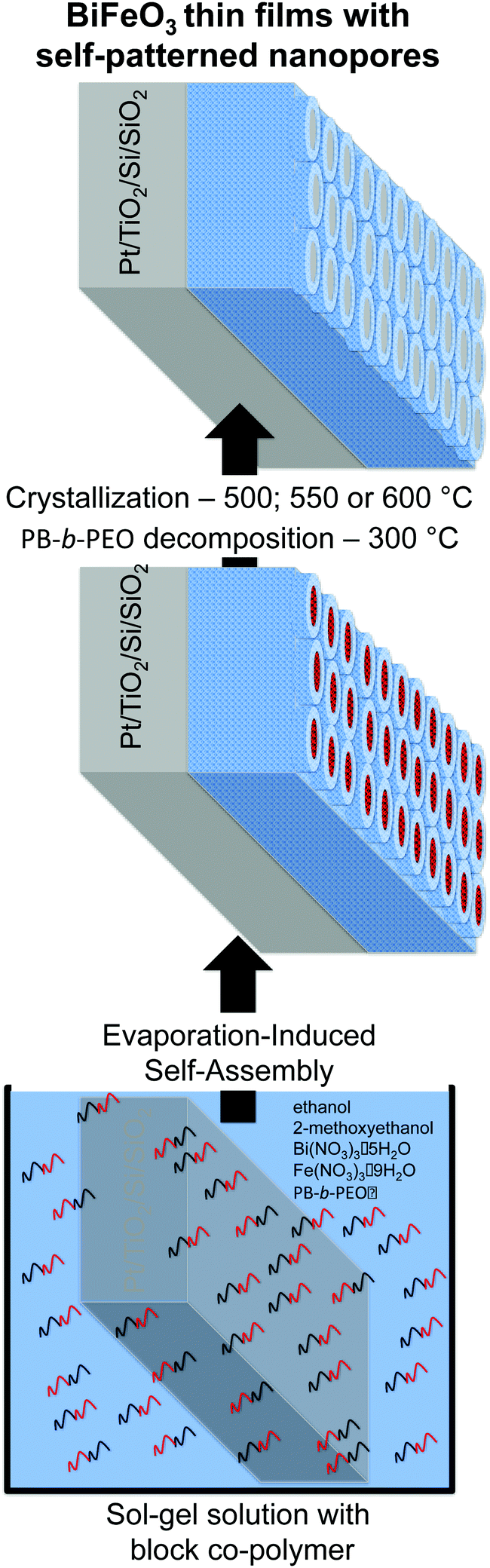 | ||
| Scheme 1 Schematic illustration of the preparation of the nanopatterned porous BiFeO3 thin films. | ||
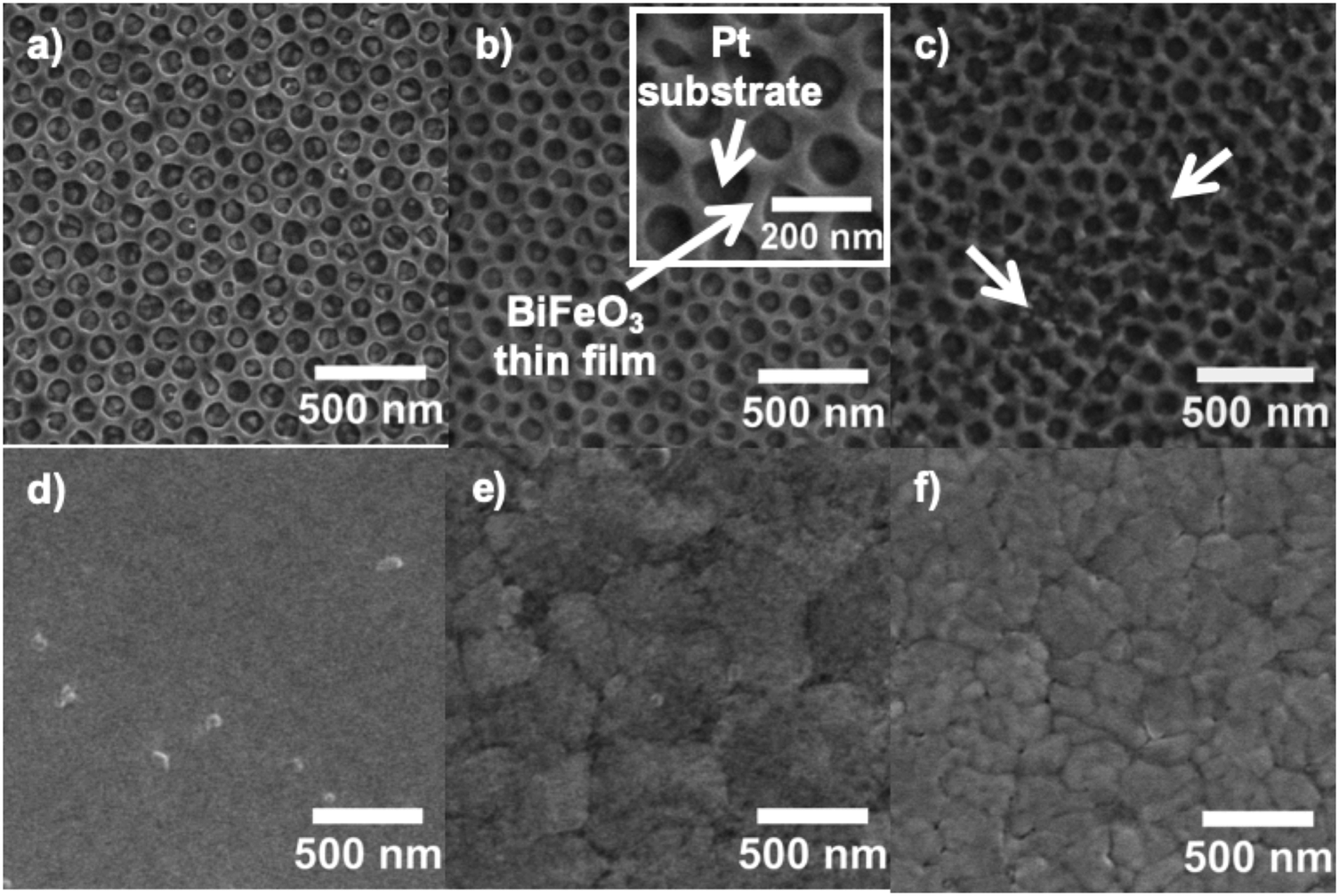 | ||
| Fig. 1 SEM micrographs of nanopatterned porous (a–c) and dense (d–f) BiFeO3 thin films thermally treated at 500 °C for 10 min (a and d), 550 °C for 5 min (b and e) and 600 °C for 5 min (c and f). The nanopatterned porous thin films show for all heating conditions well-ordered hexagonal arrays of pores (a–c). The inset in the SEM micrograph (b) shows that the pores of the nanostructure are completely empty, and that the porosity is perpendicular to the substrate. The nanopatterned thin films treated at 600 °C present some interconnected pores as shown by the white arrows, but the order and porosity at large range remain. The dense thin films present crack-free surfaces with the grain size increasing as a function of the heating temperature (d–f). | ||
The phase composition and structure of the nanopatterned porous and dense BiFeO3 thin films were analyzed by XRD for films thermally treated at 600 °C (Fig. 2). All the peaks were indexed to the perovskite-type rhombohedral structure according to JCPDS 01-075-6667, indicating practically a monophasic phase for both nanopatterned porous and dense BiFeO3 thin films. A very small peak at around 28° 2θ, and attributed to the orthorhombic pyrochlore Bi2Fe4O9 secondary phase (JCPDS 01-081-9285) can be observed in both patterns. This phase is often present in residual amounts in BiFeO3 samples. The Bi2Fe4O9 phase is known as non-ferroelectric due to the inversion symmetry structure and its high resistivity (>108 Ω cm−1), presenting paramagnetism at room temperature due to antiferromagnetism with Néel temperature of 265 K.22,23
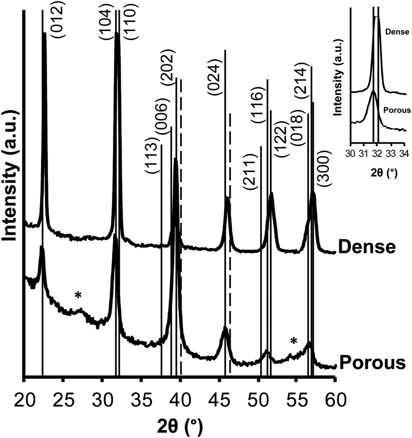 | ||
| Fig. 2 X-ray diffraction patterns of nanopatterned and dense thin films thermally treated at 600 °C. Solid black vertical lines correspond to the rhombohedral phase of BiFeO3 (JCPDS 01-075-6667) and dashed vertical lines correspond to the Pt layer of the substrate. The asterisk corresponds to the residual secondary phase, Bi2Fe4O9 (JCPDS no. 01-074-1098). The inset shows an expansion of the (104) and (110) peaks. | ||
The splitting of the peaks around 2θ 39 and 57° is indicative of the rhombohedral distortion of BiFeO3. Comparing the nanopatterned porous and dense film XRD patterns, the last ones present a profile with higher peak intensity, which can be explained by the relatively higher amount of material present in these films when compared to the nanopatterned porous ones (only ca. 43.5% of dense film).
Fig. 3 represents the topography evaluated via AFM in tapping mode of nanopatterned porous and dense BiFeO3 thin films thermally treated at 600 °C. The ordered hexagonal array of pores in the nanopatterned porous thin films (Fig. 3a and b), and well-defined grains in the dense ones (Fig. 3d and e) are easily seen from the AFM images, supporting the previous SEM observations. The line profiles (Fig. 3c and f) confirm the periodicity of pores in the nanopatterned films and the presence of grains with different sizes and heights in the dense films. Root-mean-square (RMS) roughness values are 7.3 nm and 4.3 nm for nanopatterned porous and dense films, respectively, indicating the flat surface of dense films when compared to that of the nanopatterned porous ones. Moreover, as the thin films have the same thickness, the difference in roughness supports the open porosity structure of the thin films and the availability of the pores for further functionalization.
 | ||
| Fig. 3 AFM topography images (5 μm × 5 μm and 2.5 μm × 2.5 μm) of nanopatterned porous (a and b) and dense (d and e) BiFeO3 thin films thermally treated at 600 °C. (c and f) are the line profiles along the black lines represented in (b and e). The images reveal the well-defined porous and grain structures of the nanopatterned and dense thin films, respectively. | ||
To probe the piezo and ferroelectric nature at room temperature of the nanopatterned porous and dense thin films treated at 600 °C, VPFM and PFS were carried out (Fig. 4 and 5). Though the topography images have been taken simultaneously with the mixed signal in contact mode and under the convolution effect of the tip, the porous and grain structures are clearly evident in these images (Fig. 4a and c), respectively. The results agree with the microstructure observed from SEM and AFM (Fig. 1 and 3). The application of 2 V to the films during the scan allowed us to observe the piezoelectric domains in both thin films (Fig. 4b and d). The images show the mixed signal i.e., the piezoresponse and the well-defined domain structure indicating the pronounced piezoelectric properties of both films. As these films present a low thickness, polycrystalline structure and random grain distribution as a result of the sol–gel process, the mixed signal images (Fig. 4b and d) do not display the characteristic stripe-like domains as observed for epitaxial BiFeO3 thin films with a thickness of a few hundred nanometers.8,24 On the contrary, the films present a mosaic-like structure which is similar to the results reported by Ramesh et al.25 for epitaxial BiFeO3 thin films with very low thickness (below 15 nm) and by Coondoo et al.26 for sol–gel derived BiFeO3 thin films. As the polarization in rhombohedral BiFeO3 lies along the body diagonals (111), it has three polarization directions: 71°, 109° and 180° by application of an external electrical field,25 and, consequently, its out-of-plane polarization possesses different contrasts. Bright and dark contrasts correspond to anti-parallel domains with polarization oriented towards the free surface of the films (phase = 180°) and towards the substrate (phase = −180°), respectively. Intermediate contrast corresponds to the other polarization direction. Comparing the mixed signal images of both films, one can observe that the nanopatterned porous ones have two distinct piezoelectric behaviours, corresponding to areas with strong piezoelectric response and areas where the response is almost absent. This latest observation can be associated to areas with reduced degree of crystallization, or even to size effects. The representative PFS results obtained from the strong piezoresponse domains are depicted in Fig. 5a. The piezoelectric hysteresis loops are obtained by keeping the PFM tip fixed on BiFeO3 domains and applying a bias between the conductive substrate (bottom electrode) coated with the film and the conductive AFM tip (top electrode). The voltage induces a local structural deformation due to a converse piezoelectric effect; the piezoresponse of the sample is detected by the cantilever and acquired through a lock-in amplifier circuit.27 The obtained piezoelectric hysteresis loops provide information about the switching behavior of the polarization domains. Fig. 5a shows the remnant d33 hysteresis loops of both thin films with bias from −45 to +45 V. Both nanopatterned porous and dense films display well-defined hysteresis loops, which are evidence of their ferroelectric behavior. However, and importantly, these films display different values of imprint, saturated piezoresponse and coercivity. The imprint effect is usually caused by the preference of a certain polarization state over the other. Dense films present a higher imprint effect when compared with the porous ones (Fig. 5b), which can be attributed to the presence of defects in the films, including oxygen vacancies and surface/interface defects (lattice distortion due to the difference between the thermal expansion coefficients of the film and the substrate) generating a layer of negative charge.28–30 The coercivity (here meaning the coercive field) is the required electric field strength to switch the direction of the polarization. From a statistical study of at least ten hysteresis loops for each of these films, the coercivity and the effective piezoelectric coefficient (d33)eff are estimated to be, respectively, around 5.5 ± 0.4 V and 69.8 ± 2.5 pm V−1 for the nanopatterned porous thin films, and 6.3 ± 0.9 V and 28.9 ± 1.8 pm V−1 for the dense ones (Fig. 5b). The analysis of these values shows a lower coercivity in the nanopatterned porous films, meaning that it is easier to switch the polarization in these films than in the dense ones. On the other hand, the (d33)eff value is higher for the nanopatterned porous than for the dense films. These results clearly point to the enhancement at the nanoscale of the electrical properties of the nanopatterned porous films and to the role of nano organized porosity. Comparing with the values reported in the literature, the (d33)eff value obtained for the nanopatterned porous thin film is in good agreement with the (d33)eff values reported for epitaxial BiFeO3 thin films with tetragonal phase (∼70 pm V−1)31 and for heteroepitaxially constrained BiFeO3 thin films (60 pm V−1).2,25 Furthermore, this value discloses the possibility of obtaining good piezo and ferroelectric behavior with rhombohedral structure for which the spontaneous polarization value should be significantly smaller than the expected one for a ferroelectric with such a high TC. Beyond the positive effect of the porosity on local ferroelectric properties, other possible explanations can be based on the multiferroic character of BiFeO3, the magnetoelectric coupling at the domain walls,24,32 and the symmetry breaking and the lack of homogeneity in domain walls induced by the presence of the pore. The porosity can thus lead to a reduction of the energy necessary to reorient the dipoles in the ferroelectric structures and induce instability in the dipole–dipole interaction producing a significant increase in the spontaneous polarization. In fact, this positive effect of the porosity in BiFeO3 films corroborates our previous results for nanoporous PbTiO3 thin films, in which we verified for the first time that the nanoporosity has a positive effect on the overall piezoelectric response by facilitating the domain switching.18 In addition, the better local electric properties of the nanopatterned thin films can also be related with the reduced constraining effect of the substrate when compared with that of the equivalent dense ones. The obtained (d33)eff value for dense thin films is comparable to the values previously reported for dense BiFeO3 thin films prepared by soft chemical deposition.26,33 Recently, Zhang et al.34 reported experimental and modelling studies on the effect of the macro porosity volume fraction and morphology on the polarisation-electric field response of ferroelectric bulk materials. The results of the authors corroborate the results described here as they observed that porosity up to 25% volume leads to a decrease in coercive field with increasing porosity, and this was justified by the increase of compliance of the ceramic matrix which facilitates non-180° domain switching.
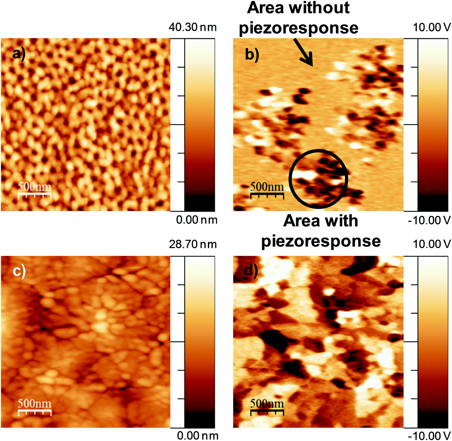 | ||
| Fig. 4 Topography and VPFM mixed signal images for nanopatterned porous (a and b) and dense (c and d) BiFeO3 thin films thermally treated at 600 °C, respectively. The data scale for VPFM mixed signal image ranges from −10 to 10 V. This 20 V scale corresponds to 360°, and thus the opposite domains oscillate 180° out of phase, as expected. | ||
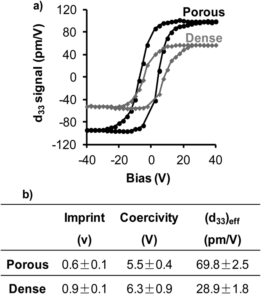 | ||
| Fig. 5 The representative remnant local hysteresis loops obtained for both thin films are presented in (a). Average values of imprint, coercivity and (d33)eff piezoelectric coefficient calculated from several mixed hysteresis loops of the nanopatterned porous and dense thin films are presented in (b). The nanopatterned porous thin films present enhanced ferroelectric properties as a consequence of their porous structure. | ||
The temperature dependence of the in-plane magnetization (magnetic field parallel to the substrate) was studied by SQUID magnetometry for both nanopatterned porous and dense BiFeO3 films thermally treated at 600 °C. The results, shown in Fig. 6a, are obtained after subtraction of the diamagnetic signal of the substrate (≈−10−7 emu g−1 Oe−1), previously measured. In these M(T) measurements, two types of procedures were used: the films were first cooled to the lowest temperature under zero magnetic field and the magnetization (ZFC curve) recorded afterwards as a function of increasing temperature, under the applied magnetic field (200 Oe); in the field cooled case (FC curve) the films were cooled under the ZFC measurement field and the magnetization measured as temperature increases, using the same rate of temperature change. In the case of dense films, the M(T) curves show an FC magnetization value that increases slightly under cooling down to 50 K, varying abruptly for the lowest temperatures assessed. The FC and ZFC curves are coincident for temperatures between 50 and 380 K but some irreversibility appears in the lowest temperature range (T < 50 K) which can be associated with a spurious residual phase not detected by XRD. For the porous film, the FC magnetization curve remains constant down to 50 K with a value around 2.7 times higher than the one observed for dense films. In contrast with the dense case, the ZFC–FC curves reveal a highly irreversible magnetic system, with a zero-field cooled magnetization that remains almost constant up to 250 K, indicating an anisotropic magnetic material where the magnetic domains remain blocked up to this temperature.
 | ||
| Fig. 6 Magnetic characterization of the dense and nanopatterned porous films. (a) ZFC curves (closed symbols) and FC curves (open symbols), measured under 200 Oe. (b) Magnetic hysteresis loops at 35 and 300 K for the dense film (inset) and the porous film, both after subtraction of the diamagnetic component. | ||
Fig. 6b shows the magnetic hysteresis loops for both films at 35 and 300 K, obtained after subtraction of the substrate diamagnetic signal. The magnetic hysteresis curves of dense films (see inset) are consistent with an antiferromagnetic behavior, as expected for BiFeO3. At both temperatures a constant magnetic susceptibility is detected for the whole magnetic field range, the higher value at 35 K being consistent with the possibility of a residual spurious phase detected in the M(T) measurements. For the nanopatterned porous film the field variation of the magnetization shows a ferromagnetic signal, leading to a saturation magnetization of 7.0(2) emu cm−3, at 300 K, with a low remnant magnetization value (0.75(1) emu cm−3) and a small coercivity (30(1) Oe). Therefore, both M(T) and M(H) measurements point to the inhibition of antiferromagnetism caused by the presence of the nano porosity and its order. Brezesinski et al.35,36 reported a preferential orientation of the magnetization as a consequence of the shape anisotropy within the pore walls for CoFe2O435 and Ho3Fe5O1236 mesoporous thin films obtained by EISA. In our case in opposition to epitaxial thin films, the magnetization orientation effect is less dependent on the substrate as stress does not result (so markedly) from a lattice or thermal expansion mismatch between the substrate and the film, but mainly from the strain of the porous structure itself.35,36
Somehow corroborating the effect on the electrical response, the nanoporosity also affects significantly the magnetic response by inhibiting the antiferromagnetic behavior of BiFeO3 films.
As BiFeO3 is a multifunctional material which can be used in several applications, the optical properties were also evaluated. Fig. 7 shows the UV-vis reflectance spectra for nanopatterned and dense BiFeO3 films thermally treated at 600 °C. The absorption of the Pt/TiO2/SiO2/Si substrate was subtracted. To determine the direct and indirect band gaps of the films, the relationship between the absorption coefficient and the incident photon energy which satisfies the Tauc representations37 was used. The (αhν)1/2versus (hν) and (αhν)2versus (hν) for both BiFeO3 thin films are plotted in Fig. 7a and b, where α and (hν) are the absorption coefficient and the incident photon energy, respectively. From a linear extrapolation of (αhν)1/2versus (hν) and (αhν)2versus (hν) plots, the indirect and direct band gaps were determined, respectively. The indirect band gaps for nanopatterned porous and dense BiFeO3 films are 2.25 eV and 2.23 eV, respectively, (Fig. 7a), while the direct band gaps are 2.58 eV and 2.39 eV, respectively (Fig. 7b). Both band gap values are located in the range of visible light and are in good agreement with other reports,19,38–40 and lower than values reported for other ferroelectric materials such as BaTiO3, and Pb(Zr,Ti)O3,4,41 which present band gaps in the ultraviolet region. The identification of band gaps in the visible range identifies BiFeO3 as an important material for solar energy conversion, photocatalysis, and artificial photosynthesis. Nanopatterned porous thin films present slightly higher direct band gap values when compared to those of dense films. This suggests that the porosity in thin films with so low a thickness induces variations in the density of states and band gaps, which can be related to quantum-confinement properties of nanocrystals.42 As reported in the literature, for thick films, around 1.5 μm in thickness, the direct band gap value is comparable to the values obtained for dense ones.40 Comparing indirect and direct band gap values, the indirect band gap usually occurs at lower energy values than the direct band gap. This observation is in accordance with previously reported results for other BiFeO3 thin films prepared by chemical methods.38,39 Furthermore, the porosity (ca. 57%) significantly increases the specific surface area.
 | ||
| Fig. 7 Plots for: (a) indirect and (b) direct optical transitions of nanopatterned porous and dense BiFeO3 thin films thermally treated at 600 °C. Extrapolation of the linear parts of the curves to zero reveals that the nanopatterned and dense thin films present a similar indirect and slightly different direct optical band gaps supporting the dependence of this property with the porosity. | ||
4. Conclusions
To the best of our knowledge, here we report for the first time the preparation of crystalline nanopatterned porous BiFeO3 thin films with pores running perpendicular to the plane, ca. 66 nm in thickness and with an average pore size of 100 nm, using a sol–gel solution and evaporation-induced self-assembly approach. The relevance of this approach lies in its simplicity, reproducibility, nonhazardous nature, cost effectiveness and suitability for producing extensive area patterns. Due to the porous structure, the nanopatterned porous thin films present enhanced electrical and magnetic properties when compared to dense counterpart films. This result allows it to be concluded that the porosity can be a way to reduce the energy necessary to reorient the dipoles in the ferroelectric structures and induce instability in the dipole–dipole interaction, thus producing a significant increase in the spontaneous polarization. In addition, the porous structure seems to inhibit the antiferromagnetic coupling leading to a stronger ferromagnetic component and remnant magnetization than that of the dense films. Hence, nanopatterned porous BiFeO3 thin films are relevant for the microelectronic industry as lead-free ferroelectric systems with tunable optimised properties for high resistive random access memories,43 actuators, etc. or as a single phase multiferroic with enhanced ferroic properties for application in spintronics and magnetic memory devices, which can be addressed electrically and magnetically.44 Moreover, nanopatterned porous films having a continuous structure of large pores are attractive structures for the development of novel and original multiferroic structures, where the magnetic behavior can be enhanced by the functionalization of the pores with a ferromagnetic material, enlarging the temperature range of application and/or increasing the magnetoelectric coupling. Additionally, due to the small band gap compared with other semiconductor materials, these nanopatterned BiFeO3 thin films can be used as novel and effective visible-light photocatalyts,45 in photovoltaic devices4 and as alternative materials for energy-related applications.Conflicts of interest
There are no conflicts to declare.Acknowledgements
This work was developed within the scope of the project CICECO-Aveiro Institute of Materials (FCT Ref. UID/CTM/50011/2019), FLEXIDEVICE (PTDC/CTM/CTM/29671/2017) and Smart Green Homes Project (POCI-01-0247-FEDER-007678) financed by national funds through the FCT/MCTES and when appropriate co-financed by FEDER under the PT2020 Partnership Agreement. AC, MAM and PF are grateful to FCT and POPH/FSE, respectively, for doctoral, post-doctoral and coordinator investigator FCT fellowships (SFRH/BD/67121/2009, SFRH/BPD/89563/2012 and IF/00300/2015-NANOTRONICS). This work was also supported by the center grant BioISI, (Ref. UID/MULTI/04046/2019) from FCT/MCTES/PIDDAC, Portugal.References
-
C. Lichtensteiger, P. Zubko, M. Stengel, P. Aguado-Puente, J.-M. Triscone, P. Ghosez and J. Junquera, Oxide Ultrathin Films: Science and Technology, 2012, pp. 1–49 Search PubMed
.
- J. Wang, J. B. Neaton, H. Zheng, V. Nagarajan, S. B. Ogale, B. Liu, D. Viehland, V. Vaithyanathan, D. G. Schlom, U. V. Waghmare, N. A. Spaldin, K. M. Rabe, M. Wuttig and R. Ramesh, Science, 2003, 299, 1719–1722 CrossRef CAS PubMed
- C. Ederer and N. A. Spaldin, Phys. Rev. B: Condens. Matter Mater. Phys., 2005, 71, 060401 CrossRef
- S. Y. Yang, L. W. Martin, S. J. Byrnes, T. E. Conry, S. R. Basu, D. Paran, L. Reichertz, J. Ihlefeld, C. Adamo, A. Melville, Y.-H. Chu, C.-H. Yang, J. L. Musfeldt, D. G. Schlom, J. W. Ager and R. Ramesh, Appl. Phys. Lett., 2009, 95, 062909 CrossRef
- L. Gao, F. Wei, Y. Zhou, X. X. Fan, Y. Wang and J. H. Zhu, Chemistry, 2009, 15, 8310–8318 CrossRef CAS PubMed
- L. Gao, S. Song, J. Ma and J. Yang, Cryst. Growth Des., 2007, 7, 895–899 CrossRef CAS
- L. W. Martin, S. P. Crane, Y.-H. Chu, M. B. Holcomb, M. Gajek, M. Huijben, C.-H. Yang, N. Balke and R. Ramesh, J. Phys.: Condens. Matter, 2008, 20, 434220 CrossRef
- G. Catalan and J. F. Scott, Adv. Mater., 2009, 21, 2463–2485 CrossRef CAS
- N. Bassiri-Gharb, Y. Bastani and A. Bernal, Chem. Soc. Rev., 2014, 43, 2125–2140 RSC
- S. M. Selbach, M.-A. Einarsrud and T. Grande, Chem. Mater., 2009, 21, 169–173 CrossRef CAS
- D. Grosso, F. Cagnol, G. J. de, A. A. Soler-Illia, E. L. Crepaldi, H. Amenitsch, A. Brunet-Bruneau, A. Bourgeois and C. Sanchez, Adv. Funct. Mater., 2004, 14, 309–322 CrossRef CAS
- N. M. Aimon, D. H. Kim, X. Sun and C. A. Ross, ACS Appl. Mater. Interfaces, 2015, 7, 2263–2268 CrossRef CAS PubMed
- R. Comes, H. Liu, M. Khokhlov, R. Kasica, J. Lu and S. A. Wolf, Nano Lett., 2012, 12, 2367–2373 CrossRef CAS PubMed
- T. Sun, Z. Pan, V. P. Dravid, Z. Wang, M.-F. Yu and J. Wang, Appl. Phys. Lett., 2006, 89, 163117 CrossRef
- N. M. Aimon, H. K. Choi, X. Y. Sun, D. H. Kim and C. A. Ross, Adv. Mater., 2014, 26, 3063–3067 CrossRef CAS PubMed
- H. K. Choi, N. M. Aimon, D. H. Kim, X. Y. Sun, J. Gwyther, I. Manners and C. A. Ross, ACS Nano, 2014, 8, 9248–9254 CrossRef CAS PubMed
- P. Ferreira, R. Z. Hou, A. Wu, M.-G. Willinger, P. M. Vilarinho, J. Mosa, C. Laberty-Robert, C. Boissière, D. Grosso and C. Sanchez, Langmuir, 2012, 28, 2944–2949 CrossRef CAS PubMed
- A. Castro, P. Ferreira, B. J. Rodriguez and P. M. Vilarinho, J. Mater. Chem. C, 2015, 3, 1035–1043 RSC
- C. Reitz, C. Suchomski, C. Weidmann and T. Brezesinski, Nano Res., 2011, 4, 414–424 CrossRef CAS
- T. E. Quickel, L. T. Schelhas, R. A. Farrell, N. Petkov, V. H. Le and S. H. Tolbert, Nat. Commun., 2015, 6, 6562 CrossRef CAS PubMed
- Q. Zhang, D. Sando and V. Nagarajan, J. Mater. Chem. C, 2016, 4, 4092–4124 RSC
- D. H. Wang and C. K. Ong, J. Appl. Phys., 2006, 100, 044111 CrossRef
- H. Naganuma, T. Okubo, K. Kamishima, K. Kakizaki, N. Hiratsuka and S. Okamura, IEEE Trans. Sonics Ultrason., 2008, 55, 1051–1055 CAS
- G. Catalan, H. Béa, S. Fusil, M. Bibes, P. Paruch, A. Barthélémy and J. Scott, Phys. Rev. Lett., 2008, 100, 027602 CrossRef CAS PubMed
- Y. H. Chu, T. Zhao, M. P. Cruz, Q. Zhan, P. L. Yang, L. W. Martin, M. Huijben, C. H. Yang, F. Zavaliche, H. Zheng and R. Ramesh, Appl. Phys. Lett., 2007, 90, 252906 CrossRef
- I. Coondoo, N. Panwar, A. Tomar, I. Bdikin, A. L. Kholkin, V. S. Puli and R. S. Katiyar, Thin Solid Films, 2012, 520, 6493–6498 CrossRef CAS
- A. Baji, Y.-W. Mai, Q. Li, S.-C. Wong, Y. Liu and Q. W. Yao, Nanotechnology, 2011, 22, 235702 CrossRef PubMed
- S. Jesse, H. N. Lee and S. V. Kalinin, Rev. Sci. Instrum., 2006, 77, 073702 CrossRef
- A. Gruverman and A. Kholkin, Rep. Prog. Phys., 2006, 69, 2443–2474 CrossRef CAS
- M. Alexe, C. Harnagea, D. Hesse and U. Gösele, Appl. Phys. Lett., 2001, 79, 242–244 CrossRef CAS
- S. Y. Yang, F. Zavaliche, L. Mohaddes-Ardabili, V. Vaithyanathan, D. G. Schlom, Y. J. Lee, Y. H. Chu, M. P. Cruz, Q. Zhan, T. Zhao and R. Ramesh, Appl. Phys. Lett., 2005, 87, 102903 CrossRef
- M. Daraktchiev, G. Catalan and J. F. Scott, Ferroelectrics, 2008, 375, 122–131 CrossRef CAS
- A. H. M. Gonzalez, A. Z. Simões, L. S. Cavalcante, E. Longo, J. A. Varela and C. S. Riccardi, Appl. Phys. Lett., 2007, 90, 052906 CrossRef
- Y. Zhang, J. Roscow, R. Lewis, H. Khanbareh, V. Y. Topolov, M. Xie and C. R. Bowen, Acta Mater., 2018, 154, 100–112 CrossRef CAS
- T. E. Quickel, V. H. Le, T. Brezesinski and S. H. Tolbert, Nano Lett., 2010, 10, 2982–2988 CrossRef CAS PubMed
- C. Suchomski, C. Reitz, D. Pajic, Z. Jaglicic, I. Djerdj and T. Brezesinski, Chem. Mater., 2014, 26, 2337–2343 CrossRef CAS
- J. Tauc, R. Grigorovic and A. Vancu, Phys. Status Solidi, 1966, 15, 627–637 CrossRef CAS
- J. F. Ihlefeld, N. J. Podraza, Z. K. Liu, R. C. Rai, X. Xu, T. Heeg, Y. B. Chen, J. Li, R. W. Collins, J. L. Musfeldt, X. Q. Pan, J. Schubert, R. Ramesh and D. G. Schlom, Appl. Phys. Lett., 2008, 92, 142908 CrossRef
- T. P. Gujar, V. R. Shinde and C. D. Lokhande, Mater. Chem. Phys., 2007, 103, 142–146 CrossRef CAS
- D. Tiwari, D. J. Fermin, T. K. Chaudhuri and A. Ray, J. Phys. Chem. C, 2015, 119, 5872–5877 CrossRef CAS
- P. S. Brody and F. Crowne, J. Electron. Mater., 1975, 4, 955–971 CrossRef CAS
- A. M. Alwan, Eng. Tech., 2007, 25, 1143–1148 Search PubMed
- Y. Wang, Z. Lv, L. Zhou, X. Chen, J. Chen, Y. Zhou, V. A. L. Roy and S.-T. Han, J. Mater. Chem. C, 2018, 6, 1600–1617 RSC
- H. Hojo, K. Oka, K. Shimizu, H. Yamamoto, R. Kawabe and M. Azuma, Adv. Mater., 2018, 30, 1705665 CrossRef PubMed
- S. J. Clark and J. Robertson, Appl. Phys. Lett., 2007, 90, 132903 CrossRef
| This journal is © The Royal Society of Chemistry 2019 |