
 Open Access Article
 This Open Access Article is licensed under a
 Creative Commons Attribution 3.0 Unported Licence
Radiative emission from Cu2ZnSnS4/ZnSn core/shell nanocrystals†
A.
Irkhina
 a,
S.
Levcenko
*a,
L.
Xie
b,
K.
Leifer
b and
T.
Unold
a
a,
S.
Levcenko
*a,
L.
Xie
b,
K.
Leifer
b and
T.
Unold
a
aDepartment Structure and Dynamics of Energy Materials, Helmholtz-Zentrum Berlin für Materialien und Energie, Berlin 14109, Germany. E-mail: sergiu.levcenco@helmholtz-berlin.de
bThe Ångström Laboratory, Department of Engineering Sciences, Uppsala University, Lägerhyddsvägen 1 Box 534, 75121 Uppsala, Sweden
First published on 23rd April 2019
Abstract
Kesterite Cu2ZnSnS4 (CZTS) nanocrystals so far have been found to luminesce neither at room temperature nor at low temperature. Here a core–shell architecture for kesterite CZTS nanocrystals is demonstrated by applying a ZnSn-alloy shell overcoating approach. These CZTS/ZnSn nanocrystals show luminescence emission at 1.05 eV, which is red-shifted by about 0.4 eV from the absorption onset and is attributed to a radiative transition involving a deep defect. Temperature-dependent photoluminescence measurements within a range of 20–200 K indicate the presence of a competing nonradiative channel with an activation energy of 50–60 meV.
Introduction
Cu2ZnSnS4 and related kesterite structure type quaternary materials have interesting potential applications in optoelectronic devices, such as photovoltaics, thermoelectrics and water-splitting.1–4 The compositional flexibility of these materials allows tuning of the band gap as well as using earth-abundant elements to tailor the electronic properties.5–7 Kesterite nanocrystals (NCs) can be readily solution processed at relatively low temperature and have been successfully employed to fabricate absorber layers of thin film solar cells with demonstrated conversion efficiencies above 9%.8,9 The syntheses of kesterite NCs are well documented in the literature and often employ the hot-injection method,5,10,11 ‘heating-up’ synthesis12 and thermal decomposition of a single-source precursor.13,14 In contrast to the large amount of available experimental data on kesterite NC growth kinetics, size and chemical composition and structure control, few studies have focused on the optical properties. There has been only one report demonstrating low temperature photoluminescence (PL) emission for sulfur and selenium containing CZTSSe nanocrystals grown in the metastable wurtzite phase,15 while the demonstration of luminescence of pure sulfur containing CZTS nanocrystals grown in the thermodynamically stable kesterite phase has been elusive. We note that the reference to kesterite-NC luminescence in ref. 16 is misleading since the luminescence in these cases actually arises from processed thin films and not from isolated NCs. It is not clear if the lack of PL emission in kesterite NCs is due to nonradiative recombination caused by intrinsic or surface defects. Although the current state of the available PL data for kesterite materials in the form of bulk or polycrystalline thin films supports the idea of significant volume nonradiative recombination leading to a low PL yield17 at room temperature, band-edge or defect-related radiative recombination is typically observed in this material.18,19 The strong effect of the unpassivated sites at the surface of nanocrystals on the optical properties has been studied for metal chalcogenide semiconductor NCs.16,20,21 A common strategy in quantum dot/nanocrystal research to eliminate surface recombination is the introduction of a core/shell structure such as demonstrated for CdSe/ZnS,22,23 CdS/CdSe24 and for ternary chalcogenides CuInSe2/ZnS.21 The inorganic shell in the ideal case provides a lattice-matched surface defect passivation layer, with a larger band gap than the NC core band gap, thus effectively confining both charge carriers in the NC. Several methods for growing a ZnS shell were developed for CuInS2 NCs, and the process parameters such as the reaction time and temperature of the core and shell, the stoichiometry of the core, the Znshell/Cu feed ratio and the type of ligand have to be optimized to improve the PL of the nanocrystals.20 For kesterite, ZnS is a natural candidate as the shell layer, because of the closely matched lattice constants allowing epitaxial growth.25 However, surface passivation can be also achieved by the formation of semiconductor/metal core/shell nanostructures with a nonepitaxial growth mechanism despite large lattice mismatches.26 In this contribution, we will demonstrate for the first time the synthesis of crystallite CZTS/amorphous ZnSn core/shell (CS) structures and show how the presence of the ZnSn shell enables the activation of radiative emission in these CZTS NCs. In addition, the influence of the Znshell/Cu feed ratio and shell temperature synthesis on the PL properties is studied and discussed.Experimental section
Materials
Copper(II) acetylacetonate (Cu(acac)2; ≥99.99% trace metal basis), zinc(II) acetate (Zn(CH3COO)2; ≥99.99% trace metal basis), tin(IV) acetate (Sn(CH3COO)4; ≥99.99% trace metal basis), elemental sulfur (powder, 99.98% trace metal basis), trioctylphosphine (TOP; technical grade, 97%), oleylamine (OAm; technical grade, 70%), oleic acid (OA; technical grade, 90%), octadecene (ODE; technical grade, 90%), hexane (≥99%), acetone (≥99.5%) and methanol (≥99.8%) were purchased from Sigma Aldrich. All chemicals were used as received without further purification.Synthesis of CZTS nanocrystals
For a typical synthesis of the core nanocrystals Cu acetylacetonate (1.32 mmol), Zn acetate (0.79 mmol), and Sn acetate (0.75 mmol) were dissolved in oleylamine (10 ml) in a three-neck flask. The mixture was heated to 100–120 °C under magnetic stirring, degassed for 30 min, backfilled with nitrogen and heated to 140 °C for 40 min followed by further heating to the injection temperature of 225 °C. Separately, a sulphur/OAm (1 M) solution was injected into the metal precursor solution. After the injection, the reaction mixture immediately changed colour to dark-brown. The system was kept at the injection temperature for 40 min, cooled down and disconnected from the heating source. The product was isolated by adding an acetone/methanol (3![[thin space (1/6-em)]](https://www.rsc.org/images/entities/char_2009.gif) :1) mixture and further centrifuging. The NCs were redispersed in 6 ml of hexane. The purification procedure was repeated at least 4 more times in order to eliminate oleylamine, unreacted precursors and by-products.
:1) mixture and further centrifuging. The NCs were redispersed in 6 ml of hexane. The purification procedure was repeated at least 4 more times in order to eliminate oleylamine, unreacted precursors and by-products.
Synthesis of the core/shell CZTS/ZnSn nanocrystals
Quasispherical CZTS nanocrystals with a Cu-poor, slightly Zn-poor composition and with an average size of 3.5 ± 0.5 nm (see the ESI,† Fig. S1) were synthesized by a hot-injection method, where zinc and tin acetates were used as metal precursors.27 For the shell growth procedure, sulfur powder was dissolved in trioctylphosphine in a glove-box at room temperature to obtain a 1 M transparent solution of tryoctylphosphine sulphide (TOPS). In the overcoating procedure, 0.5 ml of as synthesized CZTS core NCs were mixed with a zinc acetate/oleic acid (1 ml)/octadecene (8 ml) solution in a three-neck flask, which was evacuated and backfilled with nitrogen. The zinc acetate to Cu acetylacetonate (Znshell/Cu) feeding molar ratio was adjusted from 2 to 4.5 (see Table 1). Then the mixture was heated to 160 °C for 40 min. Thereafter the TOPS solution was added dropwise within 45 min to the CZTS NC containing reaction mixture (Zn/TOPS = 1/2), whereafter the temperature was kept for 15 min to allow the completion of the shell growth process. The shell growth temperature was kept at ∼160–180 °C to avoid self-nucleation of ZnS and changes of the core nanocrystals. Purification of the core/shell NCs was carried out in the same way as described for the core NCs but with a lower number of purification steps. In order to achieve effective passivation of surface defects, three types of core/shell NCs based on the same type of core NC (Tcore = 225 °C) were synthesized under different conditions as shown in Table 1.| Sample | T core (°C) | Znshell/Cu | T shell (°C) |
|---|---|---|---|
| CS1 | 200 | 2.0 | 160 |
| CS2 | 225 | 2.0 | 160 |
| CS3 | 250 | 2.0 | 160 |
| CS4 | 225 | 4.5 | 160 |
| CS5 | 225 | 4.5 | 180 |
Characterization
To analyze the structural and chemical properties of the CZTS nanocrystals, we employ the high angle annular dark field imaging technique and EDX analysis in the scanning transmission electron microscope mode on an aberration-corrected TEM, Titan Themis. The microscope was equipped with an ultra-bright XFEG electron gun, coupled with Super-X quad EDX detectors for elemental analysis. The acceleration voltage is 200 kV. The STEM-HAADF images were acquired by scanning a focused electron probe (1 Å) across the sample and recording the high angle scattered electrons on an annular detector. As the HAADF signal was generated from the different atomic planes, to a good approximation the brightest contrasts indicate the atomic columns containing Sn atoms. For the chemical analysis, the STEM-EDX technique is used. The beam current of EDX mapping for samples CS4 and CS5 was set to about 24 nA. The acquisition time was about 28 minutes. XRD measurements are performed in a grazing incidence X-ray diffraction (GIXRD) geometry using a PANalytical X’pert Pro MPD diffractometer equipped with Cu Kα-radiation (λ = 1.54056 Å). Raman measurements are carried out in the backscattering configuration on a Horiba HR800 setup at room temperature. In these measurements the 632.8 nm line of the He–Ne laser is focused on the sample by using an Olympus objective (NA = 0.1). The Raman spectra are corrected by using 638.3 and 640.2 nm lines of the calibrated lamp. The temperature-dependent PL spectra are taken in a He closed-cycle cryostat using a 660 nm laser diode as an excitation source. The PL signal is detected by a 0.5 m grating spectrometer in combination with a liquid nitrogen cooled InGaAs detector diode array. The excitation intensity is varied in the range from 0.7 to 70 W cm−2 with a set of neutral density filters. We would like to note that the upper value is chosen to avoid a heating effect evidenced by a PL emission shift to lower energy.Results and discussion
Fig. 1(a) shows the scanning transmission electron microscope high angle annular dark field (STEM-HAADF) image of the core/shell nanocrystals (CS5) obtained at 180 °C and a maximum Znshell/Cu feeding molar ratio of 4.5. Analysis of a large number of nanocrystals shows an average size of the particles of 4.4 ± 0.9 nm as depicted in the histogram in Fig. 1(b). Looking more closely at Fig. 1(a), a core/shell like structure composed of a well-crystallised nanosphere with an amorphous surface layer can be observed. The STEM image illustrates a crystal interplanar spacing within the core of 5.4 Å, which can be ascribed to the (002) plane of kesterite phase CZTS (JCPDS 00-026-0575). No lattices fringes can be observed in the shell region. The shell is completely closed and has a thickness in the range of 1–2 nm.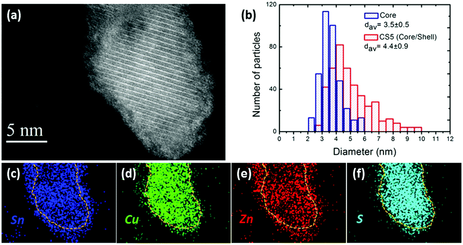 | ||
| Fig. 1 (a) STEM-HAADF image and (b) size distribution of CZTS/ZnSn core/shell NCs (b), and STEM-EDX elemental maps of core/shell NCs (c–f) using the X-ray signals of the Sn L-line, Cu K-line, Zn K-line and S K-line, respectively. | ||
Fig. 2(a) shows the results of X-ray diffraction (XRD) analysis of the initial CZTS core nanocrystals and the core/shell nanocrystals. For all samples, the diffractograms exhibit three prominent peaks which can be attributed to the kesterite CZTS (112), (220) and (312) crystal planes (JCPDS 00-026-0575), which however also coincide with corresponding reflexes of sphalerite ZnS (JCPDC 01-071-5975) and tetragonal CTS (JCPDC).
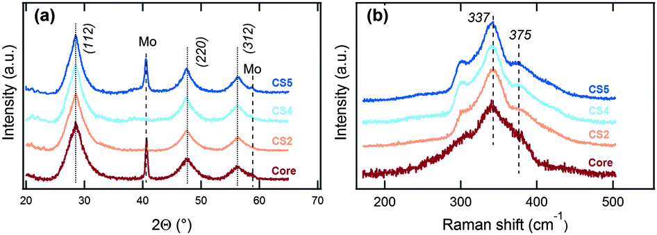 | ||
| Fig. 2 (a) XRD and (b) Raman spectra of as-grown CZTS NCs (core sample) and CZTS/ZnSn core/shell NCs (CS2, CS4 and CS5 samples). | ||
The decrease of peak broadening in the XRD pattern observed in Fig. 2(a) is consistent with an increasing average size of the corresponding core/shell nanocrystals as obtained from TEM statistics (Table 2). According to the TEM data the polydispersity of the particles increases with the shell growth. Since the growth of the shell was performed at a relatively low temperature to prevent Ostwald ripening of the core nanocrystals, the increase in NC size can be attributed to the growth of a shell layer.
| Sample | Crystallite size (nm) | Particle size (nm) |
|---|---|---|
| Core | 2.9 | 3.5 ± 0.5 |
| CS2 | 3.1 | 3.4 ± 0.6 |
| CS3 | 3.3 | — |
| CS4 | 3.7 | 4.4 ± 0.9 |
A STEM-energy dispersive X-ray (EDX) compositional analysis was applied to reveal the spatial distribution of Cu, Zn, Sn and S in the core/shell nanostructure as shown in Fig. 1(c)–(f). It can be seen that only Zn and Sn signals but no sulfur or copper are detected in the shell, from which we can conclude the formation of a Zn–Sn alloy shell. It should be noted that also no oxygen signal was observed for the shell of the NCs. Additionally, no diffraction peaks corresponding to a Zn–Sn alloy were observed in XRD, which supports an amorphous nature of the shell. The same elemental composition of the shell was found for the CS4 nanocrystals obtained at a lower shell growth temperature, which however led to a reduced shell thickness (see the ESI,† Fig, S2).
For the nanocrystal cores the TEM-EDX analysis shows a homogeneous distribution of Cu–Zn–Sn–S, indicating that these nanocrystals are composed of single phase Cu2ZnSnS4 in agreement with our previous study.27 Although XRD cannot unambiguously prove this due to the similar lattice parameters of the main secondary phases, this, however, can be resolved directly by Raman spectroscopy. Analysis of the CS nanocrystals using Raman spectroscopy shows the main kesterite peak at 337 cm−1 and a shoulder at 375 cm−1 but no secondary phase related peaks (Fig. 2(b)). In addition, the kesterite peaks become more pronounced (Fig. 2(b)) with increasing shell thickness. This could be attributed either to an increase in the CZTS nanocrystal diameter or to the improvement of the NC crystallinity. According to the XRD data the average crystallite size of the core is smaller than the average nanoparticle size obtained from TEM (Table 2), which can be explained by the fact that particles may consist of several crystallites. However, with increasing shell growth temperature and Znshell/Cu ratio the average crystallite size of the CZTS phase increased and approached the size of the initial core nanoparticles, which can be explained by an improvement of the nanoparticle crystal structure. In order to investigate whether simple annealing during the shell growth has an effect on the NC crystallinity, annealing experiments in the presence of the Zn precursor and oleic acid (but no sulfur source) were performed (see the ESI,† Fig. S3). This experiment showed that annealing alone did not change the Raman properties. Thus, we conclude that the narrowing of the Raman peaks observed after the shell growth must be due to an increase in crystallinity of the NC core caused by the shell growth process, as explained further below.
Based on the TEM and XRD observations presented above the following formation mechanism of the CS nanocrystals is suggested. As a first step, the additional Zn2+ ions can incorporate into the Zn-poor crystal structure of the CZTS core to form nanocrystals with better crystallinity and a composition closer to stoichiometry. This can occur because oleic acid has a stronger basicity than oleylamine and as a result the ligand–metal complexes can be reversibly displaced from the core surface,28,29 which can lead to vacancy formation and strong cation exchange on the surface.30 As a second step, the Sn4+, Zn2+ and Cu+ cations are reduced due to a large excess of TOP, which is well known as a good reducing agent.31 This process is expected to start with Sn4+, followed by Zn2+ because of the low reduction potential E0 (see the ESI,† Table S1). Here we assume that TOPS can detach its sulphur to provide free TOP to the reaction mixture. Since the initial composition of the core nanocrystals is slightly Sn-rich, Sn0 atoms can form a layer covering the CZTS core surface and further reduction of zinc leads to the formation of a Zn–Sn alloy on the surface, which blocks the ZnS growing process due to the large lattice mismatch. Additionally, the Zn–Sn alloy system does not form intermetallic compounds over its entire range of composition, which also inhibits sulphur incorporation into the shell.
The radiative emission properties of the CS nanocrystals were investigated by temperature-dependent PL spectroscopy. In this context, CS nanocrystals with cores synthesized at different temperatures (CS1–CS3 in Table 1) as well as CS nanocrystals based on the same core type (CS2, CS4 and CS5 in Table 1) will be discussed.
Fig. 3(a) shows the low temperature (20 K) PL for the differently synthesized CS nanocrystals. A broad PL band with a full width at a half maximum (FWHM) of about 0.35 eV centered at 1.05 eV is observed for all probed samples. There is a negligible small change in the PL maximum or FWHM between the different CS-NCs, but a clear difference in the PL yield for the NCs with different cores: CS1 (Tcore = 200 °C), CS2 (Tcore = 225 °C) and CS3 (Tcore = 250 °C), where CS1 has no detectable PL signal. For samples CS4 and CS5, the amount of Zn in the shell synthesis was increased for the same core (Tcore = 225 °C). As can be seen in Fig. 3(a) this leads to an additional increase in the PL intensity relative to the CS2 and CS3 sample types. On the other hand, it is found that the temperature of the ZnSn shell growth has little effect on the PL intensity, as seen by the identical signals observed for CS4 (Tshell = 160 °C) and CS5 (Tshell = 180 °C). It should be mentioned that in the control experiment for which Zn-rich precursors were used in the core growth, no PL signal was observed for the bare CZTS nanocrystals. Therefore, we can conclude that surface passivation of the CZTS NCs is a required step to eliminate an otherwise dominant non-radiative recombination path. The large Stokes shift (Fig. 3(b)) of the PL emission of ΔE > 0.4 eV with respect to the band gap of the CZTS core (Eg ∼ 1.5 eV)27 indicates the presence of a defect-related luminescence transition. This is in contrast to previous results of wurtzite CZTSSe nanocrystals (10–30 nm size) where no significant Stokes shift was observed,15 but is in agreement with results on CuInS2/ZnS core/shell structures where a broad PL band shifted by 0.3–0.4 eV to the lower energy region from the absorption onset was observed and attributed to a Cu related deep acceptor.21,32,33
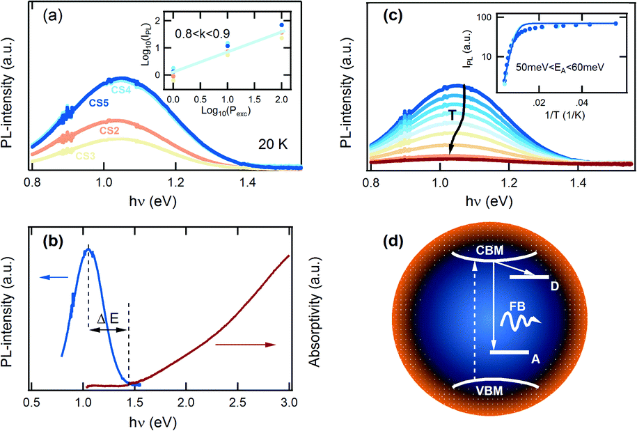 | ||
| Fig. 3 (a) PL spectra at 20 K of CZTS/ZnSn core–shell NCs. The inset illustrates the integrated PL intensity (IPL) as a function of the excitation power (Pexc) at 20 K and the solid line is a guide line plotted as IPL= Pexc0.85. (b) A comparison between PL (this work) and absorption spectra (ref. 27). (c) Temperature dependent PL emission for a CS5 sample. The inset shows the integrated PL intensity (IPL) as a function of inverse temperature (T) and the fits to a model with a single nonradiative path: IPL= I0/[1 + a1 exp(−EA/kBT)]. (d) A schematic diagram illustrating the proposed recombination mechanism for the emission in the CZTS/ZnSn core–shell NCs. | ||
We would like to point out that the FWHM and the Stokes shift between absorption and emission cannot be explained by strong electron phonon coupling.34 Considering a 1D configurational coordinate diagram with the phonons involved in the absorption and emission processes a Stokes shift ΔE ∼ 2SEph and FWHM ∼2.36EphS0.5 would be expected, where S is the Huang–Rhys factor and Eph is the phonon energy. Therefore the experimental values for CZTS nanocrystals ΔE ∼ 0.4 eV and FWHM ∼0.35 eV would correspond to S ∼ 1.8 and Eph ∼ 0.11 eV. These two values would indicate weak electron–phonon coupling and a rather large phonon energy exceeding the experimentally observed Raman-active phonon modes (Fig. 2(b)). We therefore conclude that the observed Stokes shift cannot be explained by strong electron–phonon coupling or self-trapping.
To further investigate the detailed recombination mechanism in the core/shell nanocrystals we performed excitation dependent PL measurements at low temperature. As shown (inset of Fig. 3(a)) a variation of the excitation density Pexc over 2 orders increases the PL yield but does not affect the PL maximum position, which remains at about 1.05 eV. The latter behaviour is different from the defect-related PL transitions typically observed for bulk or thin film CZTS, where a blue shift of about 5 to 20 meV per decade is usually reported.18,35 The integrated PL intensity, IPL, can be well described with a power law: IPL= Pkexc, where k is the power coefficient, which is found to be in the range 0.8–0.9 (inset of Fig. 3(a)). The obtained value of k supports a defect origin of the PL emission,36 while the lack of a shift in the PL maximum points to a free-to-bound (FB) type transition,37 possibly related to a similar mechanism to that previously proposed for CuInS2/ZnS core–shell structures: a free electron recombines with a hole localized on a deep acceptor level.21,32,33
Next, we turn to the temperature dependence of the PL emission. Fig. 3(c) shows the PL spectra obtained over the range from 18 to 200 K for sample CS5 (Tshell = 180 °C). A weak PL signal can be still detected up to temperatures of 250–260 K, albeit not at room temperature. Fig. 3(c) shows strong thermal quenching in the PL yield for temperatures above 100 K. At the same time, the PL maximum energy shifts slightly to lower energy by 10 meV and the FWHM broadens by 50 meV. From an Arrhenius plot of the integrated PL intensity versus inverse temperature (inset of Fig. 3(c)), an activation energy of 50–60 meV is determined for CZTS/ZnSn nanocrystals grown under Zn-rich conditions. Similar energy values are derived for the samples with different cores (CS2 (Tcore = 225 °C) and CS3 (Tcore = 250 °C)). Since these activation energies are much smaller than the energy depth of the deep defect involved in the radiative emission, we assign it to a different defect state acting as an effective electron trap in the competing non-radiative recombination channel,21 likely due to a residual surface state level (Fig. 3(d)).
Conclusions
A new route to improve the luminescence properties of kesterite CZTS nanocrystals is demonstrated by using a Zn–Sn overcoating technique leading to a crystalline CZTS/amorphous ZnSn core–shell structure. The CZTS/ZnSn nanocrystals exhibit a broad PL band at 1.05 eV, which we attribute to a free-to-bound transition, possibly originating from a Cu-related deep acceptor level. From the observation of PL quenching with increasing temperature, a shallow level at 50–60 meV is determined, which we associate with a surface electron trap state.Conflicts of interest
There are no conflicts to declare.Acknowledgements
A. I. acknowledges support from the MaTSEC graduate school at Helmholtz-Zentrum Berlin für Materialien und Energie.Notes and references
- M. Ibáñez, R. Zamani, A. LaLonde, D. Cadavid, W. Li, A. Shavel, J. Arbiol, J. R. Morante, S. Gorsse, G. J. Snyder and A. Cabot, J. Am. Chem. Soc., 2012, 134, 4060–4063 CrossRef PubMed.
- W. Wang, M. T. Winkler, O. Gunawan, T. Gokmen, T. K. Todorov, Y. Zhu and D. B. Mitzi, Adv. Energy Mater., 2014, 4, 1301465 CrossRef.
- M. L. Liu, I. W. Chen, F. Q. Huang and L. D. Chen, Adv. Mater., 2009, 21, 3808–3812 CrossRef CAS.
- X. Liu, Y. Feng, H. Cui, F. Liu, X. Hao, G. Conibeer, D. B. Mitzi and M. Green, Prog. Photovoltaics, 2016, 24, 879–898 Search PubMed.
- Q. Guo, H. W. Hillhouse and R. Agrawal, J. Am. Chem. Soc., 2009, 131, 11672–11673 CrossRef CAS PubMed.
- S. C. Riha, B. A. Parkinson and A. L. Prieto, J. Am. Chem. Soc., 2009, 131, 12054–12055 CrossRef CAS PubMed.
- Q. Guo, G. M. Ford, W. C. Yang, B. C. Walker, E. A. Stach, H. W. Hillhouse and R. Agrawal, J. Am. Chem. Soc., 2010, 132, 17384–17386 CrossRef CAS PubMed.
- C. J. Hages, S. Levcenco, C. K. Miskin, J. H. Alsmeier, D. Abou-Ras, R. G. Wilks, M. Bär, T. Unold and R. Agrawal, Prog. Photovoltaics, 2015, 23, 376–384 CAS.
- C. K. Miskin, W.-C. Yang, C. J. Hages, N. J. Carter, C. S. Joglekar, E. A. Stach and R. Agrawal, Prog. Photovoltaics Res. Appl., 2015, 23, 654–659 CrossRef CAS.
- C. Steinhagen, M. G. Panthani, V. Akhavan, B. Goodfellow, B. Koo and B. A. Korgel, J. Am. Chem. Soc., 2009, 131, 12554–12555 CrossRef CAS PubMed.
- Y. Zou, X. Su and J. Jiang, J. Am. Chem. Soc., 2013, 135, 18377–18384 CrossRef CAS PubMed.
- A. Shavel, M. Ibáñez, Z. Luo, J. D. Roo, A. Carrete, M. Dimitrievska, A. Genç, M. Meyns, A. Pérez-Rodríguez, M. V. Kovalenko, J. Arbiol and A. Cabot, Chem. Mater., 2016, 28, 720–726 CrossRef CAS.
- L. Arora, V. N. Singh, G. Partheepan, T. D. Senguttuvan and K. Jain, Appl. Nanosci., 2015, 1–10 Search PubMed.
- A. Khare, A. W. Wills, L. M. Ammerman, D. J. Norrisz and E. S. Aydil, Chem. Commun., 2011, 47, 11721–11723 RSC.
- A. Singh, S. Singh, S. Levcenko, T. Unold, F. Laffir and K. M. Ryan, Angew. Chem., Int. Ed., 2013, 52, 9120–9124 CrossRef CAS PubMed.
- K. E. Knowles, K. H. Hartstein, T. B. Kilburn, A. Marchioro, H. D. Nelson, P. J. Whitham and D. R. Gamelin, Chem. Rev., 2016, 116, 10820–10851 CrossRef CAS PubMed.
- C. J. Hages, A. Redinger, S. Levcenko, H. Hempel, M. J. Koeper, R. Agrawal, D. Greiner, C. A. Kaufmann and T. Unold, Adv. Energy Mater., 2017, 7, 1700167 CrossRef.
- K. Tanaka, Y. Miyamoto, H. Uchiki, K. Nakazawa and H. Araki, Phys. Status Solidi A, 2006, 203, 2891–2896 CrossRef CAS.
- S. Levcenko, V. E. Tezlevan, E. Arushanov, S. Schorr and T. Unold, Phys. Rev. B: Condens. Matter Mater. Phys., 2012, 86, 045206 CrossRef.
- M. Fu, W. Luan, S. T. Tu and L. Mleczko, Green Process. Synth., 2017, 6, 133–146 CAS.
- L. Li, A. Pandey, D. J. Werder, B. P. Khanal, J. M. Pietryga and V. I. Klimov, J. Am. Chem. Soc., 2011, 133, 1176–1179 CrossRef CAS PubMed.
- M. A. Hines and P. J. Guyot-Sionnest, J. Phys. Chem., 1996, 100, 468–471 CrossRef CAS.
- B. O. Dabbousi, J. Rodriguez, F. V. Mikulec, J. R. Heine, H. Mattoussi, R. Ober, K. F. Jensen and M. G. Bawendi, J. Phys. Chem. B, 1997, 101, 9463–9475 CrossRef CAS.
- C. Pu and X. Peng, J. Am. Chem. Soc., 2016, 138, 8134–8142 CrossRef CAS PubMed.
- N. Song, W. Li, X. Hao, Y. Huang and M. A. Green, Phys. Status Solidi RRL, 2014, 8, 404–407 CrossRef CAS.
- J. Zhang, Y. Tang, K. Lee and M. Ouyang, Science, 2010, 327, 1634–1638 CrossRef CAS PubMed.
- A. Irkhina, S. Levcenko, V. Hinrichs, P. Plate and T. Unold, RSC Adv., 2017, 7, 11752–11760 RSC.
- N. C. Anderson, M. P. Hendricks, J. J. Choi and J. S. Owen, J. Am. Chem. Soc., 2013, 135, 18536–18548 CrossRef CAS PubMed.
- H. Li, M. Zanella, A. Genovese, M. Povia, A. Falqui, C. Giannini and L. Manna, Nano Lett., 2011, 11, 4964–4970 CrossRef CAS PubMed.
- V. Lesnyak, R. Brescia, G. C. Messina and L. Manna, J. Am. Chem. Soc., 2015, 137, 9315–9323 CrossRef CAS PubMed.
- J. S. Steckel, B. K. H. Yen, D. C. Oertel and M. G. Bawendi, J. Am. Chem. Soc., 2006, 128, 13032–13033 CrossRef CAS PubMed.
- H. Zang, H. Li, N. S. Makarov, K. A. Velizhanin, K. Wu, Y.-S. Park and V. I. Klimov, Nano Lett., 2017, 17, 1787–1795 CrossRef CAS PubMed.
- W. D. Rice, H. McDaniel, V. I. Klimov and S. A. Crooker, J. Phys. Chem. Lett., 2014, 5, 4105–4109 CrossRef CAS PubMed.
- A. Alkauskas, M. D. McCluskey and C. G. Van de Walle, J. Appl. Phys., 2016, 119, 181101 CrossRef.
- T. Gershon, B. Shin, N. Bojarczuk, T. Gokmen, S. Lu and S. Guha, J. Appl. Phys., 2013, 114, 154905 CrossRef.
- T. Schmidt, K. Lischka and W. Zulehner, Phys. Rev. B: Condens. Matter Mater. Phys., 1992, 45, 8989–8994 CrossRef.
- D. M. Eagles, J. Phys. Chem. Solids, 1960, 16, 76–83 CrossRef CAS.
Footnote |
| † Electronic supplementary information (ESI) available: Additional STEM-HAADF image and STEM-EDX map of CZTS/ZnSn core/shell NCs, TEM image and Raman spectra of CZTS core NCs and reaction potential parameters. See DOI: 10.1039/c9tc00904c |
| This journal is © The Royal Society of Chemistry 2019 |