
 Open Access Article
 This Open Access Article is licensed under a
 Creative Commons Attribution 3.0 Unported Licence
An experimental and theoretical study into NaSbS2 as an emerging solar absorber
W. W. Winnie
Leung
ab,
Christopher N.
Savory
ab,
Robert G.
Palgrave
 ac and
David O.
Scanlon
*abd
ac and
David O.
Scanlon
*abd
aUniversity College London, Department of Chemistry, 20 Gordon Street, London WC1H 0AJ, UK. E-mail: d.scanlon@ucl.ac.uk
bThomas Young Centre, University College London, Gower Street, London WC1E 6BT, UK
cHarwell XPS, Room G.63, Research Complex at Harwell, Didcot, OX11 0FA, UK
dDiamond Light Source Ltd, Diamond House, Harwell Science and Innovation Campus, Didcot, Oxfordshire OX11 0DE, UK
First published on 21st January 2019
Abstract
As photovoltaics have grown to become one of the dominant renewable energy generating technologies, attention has fallen upon thin-film materials as a route to lightweight, flexible and portable solar cells. NaSbS2 has recently been proposed as a non-toxic, earth abundant solar absorber for thin-film cells. In this study, we use a combined theoretical and experimental approach to characterize and assess the electronic and optical properties of NaSbS2 as an emerging solar absorber. Our results, utilising two theoretical efficiency metrics, demonstrate that NaSbS2 may be limited for use in single-junction cells by a forbidden band gap and slow absorption onset. Other features of its electronic structure, however, indicate that the material may still be promising in thermoelectric applications.
1 Introduction
In recent decades, there has been an international drive to develop alternative renewable energy resources to replace the limited supply of fossil fuels. Solar cells represent one of the fastest-growing renewable energy markets – while the market is currently dominated by silicon cells, thin-film materials such as CdTe and Cu(InxGa1−xSe2) (CIGS) offer routes to cheap, flexible cells with lower manufacturing costs, which are useful for alternative applications to traditional rooftop panels.1,2 Despite high cell efficiencies of over 20%,3 the toxicity of Cd and the low abundance of In and Te in the earth's crust could still be major barriers to widespread, sustainable production of thin-film PV. So, there is still active research into new and promising solar absorber thin-film materials that could perform equally well as the current champions; in general, non-toxic earth abundant materials with band gaps between 1.1 eV and 1.7 eV are the most desirable targets for research for their high maximum theoretical efficiency, as well as low potential feedstock and manufacturing costs.4Ternary antimony chalcogenides such as CuSbS2 have gained rising attention in the last five years due to their non-toxicity, high earth abundancy and strong optical absorption – all suitable properties for a new sustainable material for thin film solar cells. Computational and experimental studies have reported that CuSbS2 thin films have band gaps between 1.4 eV to 1.6 eV,5–8 and an initial solar conversion efficiency of 0.5% to 3% was achieved with different prototype of CuSbS2 thin film solar cells.8–12 Other related ternary semiconductors are mostly Agx(Bi/Sb)ySez or Agx(Bi/Sb)yTez materials, where the compositions x, y and z of these compounds can be easily tuned to optimise the structural and electronic properties. These ternary semiconductors have displayed strong absorption coefficients and hence they have remained to be a popular research topic in photovoltaic applications.13–15 Given such prior success with ternary antimony semiconductors, are there other antimony chalcogenides that could possess similar properties and thus become an even better alternative solar absorber material?
Most recently, NaSbSe2 nanocrystals have been used in quantum dot-sensitized solar cells (QDSSCs) which display a relatively high solar efficiency of 2.22%.16 On the other hand, the sister compound NaSbS2, although less explored as an absorber material, also has promising features for an efficient photovoltaic material. NaSbS2 was found to have an experimental band gap value of 1.5 eV to 1.8 eV and a large absorption coefficient ∼104 cm−1 to 105 cm−1 within the visible light region.17–19 Rahayu et al. have also demonstrated a strong absorption of light in NaSbS2 coated semiconductor-sensitized solar cells, with the photovoltaic efficiency of this SSC increased from 2.30% to 3.18% under reduced light intensity.18 Furthermore, NaSbS2 quantum dot-sensitized solar cells showed to have an efficiency of 4.11%, which is the highest efficiency to date.20 Recent theoretical calculations of NaSbS2, using a Modified Becke–Johnson (MBJ) exchange potential, have shown a band gap of 1.21 eV and that it could potentially exhibit defect tolerance, as suggested by the hybridization between S p and Sb s states.21
In this work, we will explore the potential of NaSbS2 in photovoltaic applications by experimentally examining its optical and structural properties, using X-ray Diffraction, UV-Vis spectroscopy and X-ray Photoelectron Spectroscopy. Experimental properties of NaSbS2 are combined and compared with our theoretical results generated by hybrid Density Functional Theory (DFT). Our combined data show that NaSbS2 has a forbidden fundamental band gap and a poor optical absorption onset, indicating that it is less ideal for photovoltaic applications than previously proposed. Instead, the highly disperse regions around the band edges in the electronic structure of NaSbS2 and acoustic-optical phonon mixing are highly desirable for thermoelectric materials, suggesting that NaSbS2 could be a potential candidate in thermoelectric applications.
2 Methodology
2.1 Experimental synthesis
Na2S·9H2O (≥98%, Sigma-Aldrich) was first dessicated under dynamic vacuum, where there is a continuous vacuum environment ≤10−3 mbar, at 200 °C for a minimum of 2 days to obtain dehydrated Na2S. 0.2201 g of dehydrated Na2S and 0.9610 g of Sb2S3 (≥96%, Inoxia) were ground together in an agate mortar and pestle. The stoichiometric mixture was transferred in air to a quartz ampoule which was then evacuated to a pressure of ≤10−3 mbar and heated under dynamic vacuum at 550 °C for 2 h, with heating and cooling rates of 5 °C min−1.2.2 Characterization
Powder X-ray diffraction (PXRD) data was collected on a STOE diffractometer in transmission geometry using Mo Kα (0.7093 Å) radiation over the 2θ range of 2° to 40° with a step size of 0.02° at 20 s per step. Optical diffuse-reflectance spectroscopy was measured between 250 nm to 2000 nm with a step size of 1 nm using PerkinElmer Fourier Transform Lambda 950 UV-Vis spectrophotometer equipped with an integrating sphere at ambient temperature. X-ray photoelectron spectroscopy (XPS) was also performed using a Thermo Scientific Kα spectrometer utilizing a 72 W Al Kα X-ray source. High resolution scans with a binding energy step size of 0.1 eV was used and in situ Ar ion etching was performed using a 2 keV Ar ion beam in a background Ar pressure of 2 × 10⁻⁷. The binding energy scale was corrected for charing by adjusting the adventitious C 1s peak to 284.8 eV. Conductivity measurements were performed using an Ecopia HMS-3000 instrument and a van der Pauw electrode geometry.2.3 Theoretical
Density Functional Theory (DFT) calculations were performed on NaSbS2 within periodic boundary conditions through the Vienna Ab Initio Simulation Package (VASP).22–25 The screened hybrid functional HSE06 was used to relax the structure into its equilibrium geometry.26 HSE06, with the explicit addition of spin–orbit coupling (HSE06 + SOC), was then used to calculate the electronic density of states, band structure and optical properties. HSE06 includes 25% Hartree–Fock exchange at short range, determined by a screening parameter of ω = 0.11 bohr−1, with 75% exchange and 100% correlation from the GGA-functional PBE,27 returning to entirely PBE at long ranges. HSE06 has been used successfully to describe the structure and electronics of ternary antimony chalcogenides in previous studies.28–30 The projector-augmented wave (PAW) method is used to describe valence-core electron interactions,31 and scalar-relativistic pseudopotentials were used. A plane-wave cutoff energy of 350 eV and k-point mesh of 6 × 6 × 6 were used for the relaxation and electronic calculations, and were sufficient to converge the total energy to within 1 meV per atom.During the relaxation, the forces on each atom were reduced to below 0.01 eV Å−1, and the cutoff was increased by 40% to avoid errors relating to Pulay stress. Convergence of the optical spectrum and SLME with respect to k-mesh was checked using HSE06 calculations of increasing k-point density up to 12 × 12 × 12, and it was found that a mesh of 6 × 6 × 6 was sufficient for accurate optical properties, so this mesh was used for the HSE06 + SOC optical calculations. The optical calculations were performed within the method of Furthmüller et al.32 Additional calculations were performed on a 4 × 4 × 4 supercell to construct the phonon dispersion curve for NaSbS2 using the finite differences method within the PHONOPY package.33 Given the expense of HSE06, these displacements were instead performed with the PBEsol functional, which has been used previously to accurately describe the structural properties of bismuth and antimony-based semiconductors.34–36 The displacement calculations used a higher energy cutoff of 550 eV and convergence of 10−8 eV on the total energy to ensure sufficient accuracy in the calculation of the second-order force constants. Crystal structures were depicted using the program VESTA,37 while plots of the electronic and optical properties made use of the sumo package.38
3 Results and discussions
3.1 Structure
Fig. 1 shows the structure of NaSbS2, which is monoclinic, and consists of [4+2] Sb–S chains, with the sodium sitting in a distorted octahedral environment. A structural model in the C2/c space group was refined against the PXRD data using the Rietveld method on GSAS and EXPGUI software. Fig. 2 shows that as-synthesised NaSbS2 powders are phase pure and the experimental and calculated powder X-ray diffraction pattern from Rietveld refinement of NaSbS2.39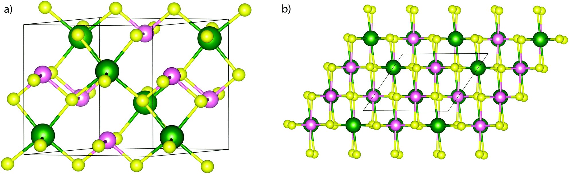 | ||
| Fig. 1 (a) Unit cell diagram of NaSbS2 with C2/c space group and (b) the structure viewed along (010), demonstrating the similarity to the rock salt structure. The Na atoms are marked in green, Sb in pink and S in yellow, with the unit cell boundary marked in black; only the short Sb–S bonds are drawn in. | ||
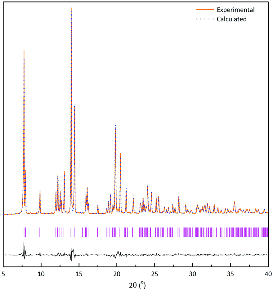 | ||
| Fig. 2 XRD pattern of as-synthesized NaSbS2 powder and calculated pattern from rietveld refinement with the difference between the experimental and calculated XRD shown in black. Positions of each reflection are shown in pink. | ||
Lattice parameters of as-synthesized NaSbS2 crystal structure were obtained during Rietveld refinement, and all values are in good agreement with the standard NaSbS2 structure,39 which are shown in Table 1.
| Experimental NaSbS2 (Å) | Standard NaSbS239 (Å) | |
|---|---|---|
| a | 8.249(1) | 8.232(1) |
| b | 8.278(1) | 8.252(2) |
| c | 6.851(1) | 6.836(1) |
The computational relaxation of NaSbS2, starting from the standard structure recorded by Fourcade et al., using the HSE06 functional resulted in the equilibrium lattice parameters included in Table 2. These parameters show only very slight (<1.5%) expansion in a and b, and similar contraction in c in comparison with our synthesised sample, as well as similar deviation from the Fourcade structure. Through this, the HSE06 functional appears to provide an accurate description of the room temperature structural properties.
| HSE06 (Å)/° | % difference from | ||
|---|---|---|---|
| As-synthesised NaSbS2 | Fourcade et al.39 | ||
| a | 8.2612 | +0.15 | +0.35 |
| b | 8.3931 | +1.39 | +1.71 |
| c | 6.8209 | −0.43 | −0.22 |
| β | 124.15 | −0.10 | |
3.2 Electronic structure
XPS spectra of NaSbS2 are shown above together with the curve fitting. The background was modelled using a Shirley function and spectral components were modelled using a convolution of Gaussian and Lorentzian functions. Where appropriate, these components were constrained according to the expected intensity raitos and splitting constants for spin orbit doublets. The as-synthesized powder sample was etched for 10 min, using a 2 keV Ar ion beam, to significantly reduce the amount of oxygen on the surface. Fig. 3 shows a symmetrical Na 1s peak at 1071.5 eV corresponding to Na(I) can be observed in the high resolution scan. In the same figure the Sb 3d spectra consists of a spin–orbit doublet, the higher binding energy component Sb 3d3/2 at 539.8 eV and lower binding energy component Sb 3d5/2, at 530.4 eV, which overlaps with O 1s regions. Due to the indistinguishable nature of Sb(III) and Sb(V) species on the surface, it is possible that both species co-exist on the surface. However, the presence of Sb(V) in the as-synthesized NaSbS2 powder would cause the unit cell lattice to shrink as it has a smaller ionic radius (0.60 Å) than Sb(III) (0.76 Å), the refined experimental lattice parameters shown previously suggested that only Sb(III) are present in the bulk of as-synthesized powder.40 The significantly reduced amount of oxygen can be accounted for the small trace shoulder region visible in the Sb 3d5/2 component of the etched NaSbS2 sample whereas a much larger shoulder region was observed in the same region of the non-etched NaSbS2 sample. S 2p spectrum shown in Fig. 3 was composed of an overlapping spin–orbit doublet, the lower binding energy component S 2p3/2 peak at 162.2 eV is consistent with expectations for S2− ions,41 whereas the higher binding energy component corresponding to sulfate species was not observed after etching. | ||
| Fig. 3 X-ray photoelectron spectra showing (a) Na 1s and (b) Sb 3d with overlapping O 1s regions, (c) S 2p and (d) the valence band region overlayed with simulated valence band data. | ||
The electronic Density of States (DOS), calculated using HSE06 + SOC, of NaSbS2 is included in Fig. 4. The overall trend and composition in the density of states is similar to many other ns2 absorber materials: the valence band is dominated by the anion p and antimony p, while antimony s appears at the very top – this mixing of cation s and anion p in an anti-bonding fashion (with stabilisation from the cation p) is consistent with the revised lone pair model proposed by Walsh et al.,42 and is also reflected in the crystal through a stereochemically active lone pair on the antimony. While NaSbS2 shares overall structural similarities with a rock salt structure, the C2/c ground state can be viewed as a distortion from a perfect octahedral (rock salt) cation environment to a [4+2] Sb environment due to the active lone pair occupying part of the coordination sphere. The conduction band in further accordance with the model is then dominated by the Sb p and S p. As discussed, these contributions are common to many lone pair materials, for example NaSbS2's stoichiometric counterpart, CuSbS2. Despite occupying very different crystal structures, the valence band of CuSbS2 is also composed of S p, Sb s and Sb p states (albeit with the addition of Cu d) and the conduction band is primarily composed of Sb p and S p.29,43 As has been done previously for CuSbS2,43 the density of states, when scaled by photoionisation cross-sections and smeared to replicate experimental broadening, matches well to our valence band XPS shown in Fig. 3, demonstrating the suitability of the HSE06 + SOC functional at describing these states. This strong match also includes the lower energy bands (at a binding energy of ∼−11 eV), which are the corresponding bonding states between Sb s and S s and p. The qualitative electronic similarities between CuSbS2 and NaSbS2 begin to break down, however, when we look at the band structure, and the influence of the crystal structure becomes apparent.
 | ||
| Fig. 4 Electronic density of states of NaSbS2, calculated using HSE06 + SOC; E = 0 is set to the valence band maximum. | ||
The electronic band structure of NaSbS2 is plotted in Fig. 5. The fundamental band gap is direct, occurring at the Y point, and has a magnitude of 1.585 eV. This is both close to the ideal range we would aim for to maximise the theoretical efficiency (∼1.0 eV to 1.5 eV) but also close to our experimentally recorded optical gap of 1.73 eV. The fundamental band gap is also consistent with the Bhattacharya et al.'s band gap of 1.58 eV, which was obtained using Engler-Vosko LAPW method.44 Both the valence and conduction bands show a mix of highly disperse regions around the band edges with comparatively flat regions elsewhere, to the extreme where the conduction band at M is nearly degenerate with the conduction band minimum at Y. This form of structure is often described as ‘multi-valley’, and has been highlighted in previous studies for allowing both good carrier mobility and relatively high joint density of states, enabling strong absorption – two properties that are both highly desirable for photovoltaic absorber materials, but which can sometimes be mutually exclusive.4,36 Notably, while the magnitude of the spin–orbit coupling is small in this system (antimony is light in comparison to the cations used in other ns2 solar absorbers), its inclusion is crucial for this direct gap behaviour: using HSE06 alone, the conduction band separation at Y is lessened, the CBM instead occurs at M, and so the band gap becomes indirect by 18 meV.
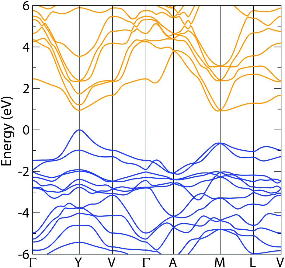 | ||
| Fig. 5 Electronic band structure of NaSbS2, calculated using HSE06 + SOC; valence band is in blue, conduction band in orange and E = 0 is set to the valence band maximum. The notation of Bradley and Cracknell is used for identifying special k-points in the C2/c Brillouin zone.45 | ||
3.3 Electrical properties
In order to measure the electrical conductivity of NaSbS2, as-synthesized powder was pressed into two pellets, A and B. Pellet A was measured directly using a four point probe Hall machine and pellet B was sintered at 400 °C for 2 h in prior to the measurement. The Hall voltage induced, under a magnetic flux density of 0.58 T, in both pellets were negligible, causing the results to be unreliable. Alternatively, molten NaSbS2 was obtained upon heating at 800 °C and it was also measured on the Hall machine, yet the Hall voltage was too small to give any reliable and accurate data. As a result, it is highly likely that stoichiometric NaSbS2 powders synthesised in this method are non-conductive. Future work can be done on densifying the pellets to minimise the effects of grain boundaries, changing the stoichiometry of NaSbS2 and modifying the synthesis method.The hole and electron effective masses were estimated from the HSE06 + SOC band structure of NaSbS2 using a parabolic fit to the band edges, and are recorded in Table 3. The local dispersion at the band edges means that the effective masses of both holes and electrons are low and, indeed, reasonably ideal for an absorber material.46 Despite the distortion of the structure away from a perfect rock salt due to the lone pair on antimony, the effective masses are also quite isotropic in both the conduction and valence bands. One might expect such effective masses to be reflected by high carrier mobilities in a Hall effect measurement, however with our stoichiometric samples not demonstrating sufficient conductivity, this comparison is not possible.
| Valence band (m0) | Conduction band (m0) | ||
|---|---|---|---|
| Y → Γ | Y → V | Y → Γ | Y → V |
| −0.346 | −0.391 | 0.342 | 0.372 |
3.4 Optical properties
Diffuse-reflectance measurements were transformed using Kubelka–Munk function, F(R), which is considered to be proportional to absorption assuming that the scattering is constant throughout the wavelength range used in the measurement.47 Poeppelmeier and his team have proposed a method for accurate determination of the band gap in crystalline and degenerately-doped semiconductors, the major difference between Poeppelmeier and the conventional Tauc method is that Poeppelmeier takes into account the presence of a large concentration of charge carriers in crystalline materials whereas Tauc method was originally used to assess amorphous materials.48,49Fig. 6 shows the plots of F(R) and F(R)2 where each of the absorption edges was extrapolated to the x-axis (y = 0), giving values of E1 and E2 respectively. According to the Poeppelmeier method, the optical band gap value (Eg) can be calculated using 2E2 − E1, giving NaSbS2 a band gap of 1.73 eV, which is consistent with the experimental band gap of NaSbS2 nanoparticles (∼1.7 eV) demonstrated by Rahayu et al.18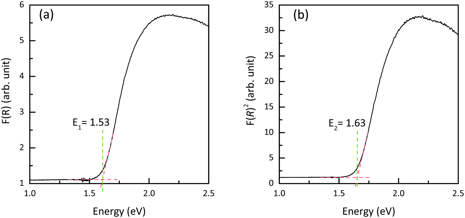 | ||
| Fig. 6 Plots of (a) F(R) and (b) F(R)2 of NaSbS2. | ||
We can then compare to the theoretical optical behaviour of the system – the absorption coefficient, calculated using HSE06 + SOC, is plotted in Fig. 7. Unfortunately, while the absorption is strong (above 105 cm−1) for energies above 2.5 eV, it is much lower in the crucial energy range just above the fundamental gap (represented by the dashed line). This low absorption originates from forbidden transitions (defined here as having a transition amplitude <0.0001): both of the direct transitions from VBM to CBM and from the VBM to the next conduction band at Y (the next-lowest energy transition) are forbidden in this way. Instead, transitions are allowed from valence to conduction band along the Y to V, however the dispersion of these bands mean that the lowest direct transition is not available until 1.77 eV. This is then representative of a theoretical optical gap, and correlates very well with our optical gap from diffuse-reflectance above. These forbidden transitions, and resultant low absorption coefficient in a crucial region of the solar spectrum, could have significant impact on the material's ability to act as a useful photovoltaic absorber, particularly within a ‘thin-film’ style architecture.
 | ||
| Fig. 7 Optical absorption coefficient (solid blue line) of NaSbS2, calculated using HSE06 + SOC. The position of the fundamental band gap is marked by the dotted line. | ||
In order to assess how badly these optical losses may affect NaSbS2, we can calculate metrics that take such properties into account, such as Spectroscopically Limited Maximum Efficiency (SLME), as designed by Yu and Zunger.50,51 With a difference of ∼0.2 eV between the lowest allowed transition and the fundamental gap, coupled with weak optical absorption, the SLME of NaSbS2 is calculated to be 11.50% for a film thickness (L) of 200 nm; such a value compares poorly with other proven and emerging solar absorbers, which often have SLME above 20%.35,51,52 Another metric for screening photovoltaic materials has recently been proposed by Blank et al., which also includes the refractive index as a crucial parameter that influences the resultant external properties, such as the current density, in the calculation of a theoretical efficiency limit.53 The Blank et al. model also uses the internal luminescence quantum efficiency (Qi, the proportion of total recombination that is radiative) as a free parameter, and so a range of values were calculated for NaSbS2, for a 200 nm thickness, and recorded in Table 4.
| Q i | Flat front surface | Lambertian scatterer | ||
|---|---|---|---|---|
| η at 200 nm (%) | Optimal L (m) | η at 200 nm (%) | Optimal L (m) | |
| 1 | 13.3 | — | 22.3 | — |
| 10−3 | 11.2 | 1.39 × 10⁻⁴ | 19.8 | 1.94 × 10⁻⁵ |
| 10−5 | 10.1 | 1.00 × 10⁻⁴ | 17.8 | 1.39 × 10⁻⁵ |
| 10−7 | 8.98 | 1.00 × 10⁻⁴ | 15.9 | 1.39 × 10⁻⁵ |
The refractive index of NaSbS2 is moderate, and so the predicted efficiency differs significantly whether the front surface of the absorber is modelled as flat, or as a Lambertian scatterer: the flat surface values give a low efficiency, similar to the SLME value, even at high values of Qi; the efficiencies from the Lambertian model are more promising, although only exceed 20% near the radiative limit. Table 4 also contains, for the given Qi, the ‘optimal’ thickness of absorber (the thickness needed to give the maximum overall efficiency) – while these thicknesses provide maximum efficiency values between 20% to 25%, comparable to those of promising absorbers,53 the inherent limitation of the absorption coefficient of NaSbS2 is evident in that ∼10 μm to 100 μm of material, as opposed to nm, is required to achieve such efficiencies.
Within both metrics, bulk NaSbS2 is not predicted to be able to reach optimal efficiencies within a thin-film style architecture, and so while the initial moderate efficiency cells being produced are promising, further progress may be limited unless relative thick layers of material are used. The influence of the surface scattering is also predicted to be relatively strong, and so texturing of a film surface or retention of nano-scale architectures may aid cell efficiencies.
Finally, the phonon dispersion curve of NaSbS2 was calculated to ensure that it is dynamically stable within the C2/c structure – the resultant curve is shown in Fig. 8. The lack of any imaginary modes demonstrates the dynamic stability of the C2/c structure, and thus shows that the distortions from an ideal rock-salt are a realistic description of the low-temperature behaviour of NaSbS2. Given the above results reflecting its poor optical behaviour however, we may also consider this spectrum in the context of other proposed applications, namely as a thermoelectric. The ABX2 (A = Ag, Na; B = Sb, Bi; X = Se, Te) compounds, which have a rocksalt structure with 1+ and 3+ cations distributed over the cation site, have been previously noted to have promising low lattice thermal conductivities due to the behaviour of the Sb lone pair.54,55 NaSbS2, with the stereochemically active lone pair demonstrable in the structure, is likely to follow similar behaviour: the acoustic phonon modes visible in the dispersion curve are somewhat flat, and there is some mixing of these modes with lower frequency optical modes – this mixing has been highlighted as characteristic of a number of other lone-pair materials, as well as beneficial for low lattice thermal conductivities.56,57
 | ||
| Fig. 8 Phonon dispersion curve of NaSbS2, calculated using the PBEsol functional. | ||
4 Conclusion
Phase pure NaSbS2 powders were synthesised and our experimental and theoretical lattice parameters agree well with previous reports. The electronic band structure of NaSbS2, calculated using the HSE06 + SOC functional, demonstrates a direct fundamental band gap of 1.59 eV and a theoretical optical gap of 1.77 eV, which is consistent with the band gap of 1.73 eV extracted from UV-Vis measurements via the Poeppelmeier method, higher than ideal for a single-junction absorber. Our calculations have also demonstrated a relatively low absorption coefficient just above the band gap in NaSbS2 due to forbidden transitions at the Y point. Combining this information, the SLME of NaSbS2 is found to be 11.5% assuming a film thickness of 200 nm, which is significantly lower than 20%, the typical value for other champion solar absorbers; calculation of the more recent metric of Blank et al. demonstrates that efficiency improvement may only be possible using a thicker film or surface engineering. With such detrimental optical properties, NaSbS2 does not seem feasible for single-junction photovoltaic applications. The electronic band structure does, however, show areas of both low and high dispersion, together with near-degenerate points within the conduction band at Y and M; a multi-valley band structure such as this has been linked to optimal thermoelectric behaviour, and so NaSbS2 may have more success in thermoelectric devices.Conflicts of interest
There are no conflicts to declare.Acknowledgements
WWL and CNS acknowledge the Department of Chemistry at UCL for the provision of DTA studentships. DOS acknowledges support from the SUPERSOLAR SolarEnergy Hub (EP/J017361/1) for the provision of a flexible funding call award and membership of the Materials Design Network. XPS data collection was performed at the EPSRC National Facility for XPS (‘HarwellXPS’) under contract No. PR16195. This work made use of the ARCHER UK National Supercomputing Service (http://www.archer.ac.uk), via our membership of the UK's HEC Materials Chemistry Consortium, which is funded by EPSRC (EP/L000202) in addition to the UCL Grace (Grace@UCL) and Legion (Legion@UCL) HPC Facilities. The authors are extremely grateful to Prof. T. Kirchartz for the provision of scripts allowing the calculation of the Blank et al. selection metric.Notes and references
- L. M. Peter, Philos. Trans. R. Soc., A, 2011, 369, 1840–1856 CrossRef CAS PubMed.
- N. M. Haegel, R. Margolis, T. Buonassisi, D. Feldman, A. Froitzheim, R. Garabedian, M. Green, S. Glunz, H.-M. Henning, B. Holder, I. Kaizuka, B. Kroposki, K. Matsubara, S. Niki, K. Sakurai, R. A. Schindler, W. Tumas, E. R. Weber, G. Wilson, M. Woodhouse and S. Kurtz, Science, 2017, 356, 141–143 CrossRef CAS PubMed.
- M. A. Green, Y. Hishikawa, E. D. Dunlop, D. H. Levi, J. Hohl-Ebinger and A. W. Ho-Baillie, Prog. Photovoltaics Res. Appl., 2017, 26, 3–12 CrossRef.
- A. M. Ganose, C. N. Savory and D. O. Scanlon, Chem. Commun., 2017, 53, 20–44 RSC.
- Y. Rodrìguez-Lazcano, M. T. S. Nair and P. K. Nair, J. Electrochem. Soc., 2005, 152, G635 CrossRef.
- J. Zhou, G.-Q. Bian, Q.-Y. Zhu, Y. Zhang, C.-Y. Li and J. Dai, J. Solid State Chem., 2009, 182, 259–264 CrossRef CAS.
- J. T. Dufton, A. Walsh, P. M. Panchmatia, L. M. Peter, D. Colombara and M. S. Islam, Phys. Chem. Chem. Phys., 2012, 14, 7229–7233 RSC.
- B. Yang, L. Wang, J. Han, Y. Zhou, H. Song, S. Chen, J. Zhong, L. Lv, D. Niu and J. Tang, Chem. Mater., 2014, 26, 3135–3143 CrossRef CAS.
- W. Septina, S. Ikeda, Y. Iga, T. Harada and M. Matsumura, Thin Solid Films, 2014, 550, 700–704 CrossRef CAS.
- B. Krishnan, S. Shaji and R. E. Ornelas, J. Mater. Sci.: Mater. Electron., 2015, 26, 4770–4781 CrossRef CAS.
- F. W. de Souza Lucas, A. W. Welch, L. L. Baranowski, P. C. Dippo, H. Hempel, T. Unold, R. Eichberger, B. Blank, U. Rau and L. H. Mascaro, et al. , J. Phys. Chem. C, 2016, 120, 18377–18385 CrossRef CAS.
- S. Banu, S. J. Ahn, S. K. Ahn, K. Yoon and A. Cho, Sol. Energy Mater. Sol. Cells, 2016, 151, 14–23 CrossRef CAS.
- S. Zhou, J. Yang, W. Li, Q. Jiang, Y. Luo, D. Zhang, Z. Zhou and X. Li, J. Electrochem. Soc., 2016, 163, D63–D67 CrossRef CAS.
- M. Bernechea, N. C. Miller, G. Xercavins, D. So, A. Stavrinadis and G. Konstantatos, Nat. Photonics, 2016, 10, 521–525 CrossRef CAS.
- F. Viñes, M. Bernechea, G. Konstantatos and F. Illas, Phys. Rev. B, 2016, 94, 235203 CrossRef.
- B. A. Aragaw, J. Sun, D. J. Singh and M.-W. Lee, RSC Adv., 2017, 7, 45470–45477 RSC.
- V. A. Bazakutsa, N. I. Gnidash, A. K. Kul'chitskaya and A. V. Salov, Soviet Physics Journal, 1975, 18, 472 CrossRef.
- S. U. Rahayu, C.-L. Chou, N. Suriyawong, B. A. Aragaw, J.-B. Shi and M.-W. Lee, APL Mater., 2016, 4, 116103 CrossRef.
- Z. Xia, F.-X. Yu, S.-C. Lu, D.-J. Xue, Y.-S. He, B. Yang, C. Wang, R.-Q. Ding, J. Zhong and J. Tang, Chin. Chem. Lett., 2017, 28, 881–887 CrossRef CAS.
- W.-C. Sun, S. U. Rahayu and M.-W. Lee, IEEE Journal of Photovoltaics, 2018, 8, 1011–1016 Search PubMed.
- J. Sun and D. J. Singh, Phys. Rev. Appl., 2017, 7, 024015 CrossRef.
- G. Kresse and J. Hafner, Phys. Rev. B: Condens. Matter Mater. Phys., 1993, 47, 558 CrossRef CAS.
- G. Kresse and J. Hafner, Phys. Rev. B: Condens. Matter Mater. Phys., 1994, 49, 14251 CrossRef CAS.
- G. Kresse and J. Furthmüller, Phys. Rev. B: Condens. Matter Mater. Phys., 1996, 54, 11169 CrossRef CAS.
- G. Kresse and J. Furthmüller, Comput. Mater. Sci., 1996, 6, 15–50 CrossRef CAS.
- A. V. Krukau, O. A. Vydrov, A. F. Izmaylov and G. E. Scuseria, J. Chem. Phys., 2006, 125, 224106 CrossRef PubMed.
- J. Perdew, K. Burke and M. Ernzerhof, Phys. Rev. Lett., 1996, 77, 3865–3868 CrossRef CAS PubMed.
- M. Kumar and C. Persson, J. Renewable Sustainable Energy, 2013, 5, 031616 CrossRef.
- D. J. Temple, A. B. Kehoe, J. P. Allen, G. W. Watson and D. O. Scanlon, J. Phys. Chem. C, 2012, 2, 7334–7340 CrossRef.
- M. Birkett, C. N. Savory, M. K. Rajpalke, W. M. Linhart, T. J. Whittles, J. T. Gibbon, A. W. Welch, I. Z. Mitrovic, A. Zakutayev, D. O. Scanlon and T. D. Veal, APL Mater., 2018, 6, 084904 CrossRef.
- P. Blochl, Phys. Rev. B: Condens. Matter Mater. Phys., 1994, 50, 17953–17979 CrossRef.
- M. Gajdoš, K. Hummer, G. Kresse, J. Furthmüller and F. Bechstedt, Phys. Rev. B: Condens. Matter Mater. Phys., 2006, 73, 045112 CrossRef.
- A. Togo and I. Tanaka, Scr. Mater., 2015, 108, 1–5 CrossRef CAS.
- K. K. Bass, L. Estergreen, C. N. Savory, J. Buckeridge, D. O. Scanlon, P. I. Djurovich, S. E. Bradforth, M. E. Thompson and B. C. Melot, Inorg. Chem., 2017, 56, 42–45 CrossRef CAS PubMed.
- C. N. Savory, A. M. Ganose and D. O. Scanlon, Chem. Mater., 2017, 29, 5156–5167 CrossRef CAS.
- R. X. Yang, K. T. Butler and A. Walsh, J. Phys. Chem. Lett., 2015, 6, 5009–5014 CrossRef CAS PubMed.
- K. Momma and F. Izumi, J. Appl. Crystallogr., 2011, 44, 1272–1276 CrossRef CAS.
- A. M. Ganose, A. J. Jackson and D. O. Scanlon, J. Open Source Software, 2018, 3, 717 CrossRef.
- J. Olivier-Fourcade, E. Philippot and M. Maurin, Z. Anorg. Allg. Chem., 1978, 446, 159–168 CrossRef.
- R. Shannon and C. Prewitt, J. Inorg. Nucl. Chem., 1970, 32, 1427–1441 CrossRef CAS.
- M. Descostes, F. Mercier, N. Thromat, C. Beaucaire and M. Gautier-Soyer, Appl. Surf. Sci., 2000, 165, 288–302 CrossRef CAS.
- A. Walsh, D. J. Payne, R. G. Egdell and G. W. Watson, Chem. Soc. Rev., 2011, 40, 4455–4463 RSC.
- T. J. Whittles, T. D. Veal, C. N. Savory, A. W. Welch, F. W. de Souza Lucas, J. T. Gibbon, M. Birkett, R. J. Potter, D. O. Scanlon, A. Zakutayev and V. R. Dhanak, ACS Appl. Mater. Interfaces, 2017, 9, 41916–41926 CrossRef CAS PubMed.
- S. Bhattacharya, R. Chmielowski, G. Dennler and G. K. H. Madsen, J. Mater. Chem. A, 2016, 4, 11086–11093 RSC.
- C. J. Bradley and A. P. Cracknell, Mathematical Theory of Symmetry in Solids, Oxford University Press, 1972 Search PubMed.
- G. Hautier, A. Miglio, D. Waroquiers, G.-M. Rignanese and X. Gonze, Chem. Mater., 2014, 26, 5447–5458 CrossRef CAS.
- P. Kubelka, Z. Tech. Phys., 1931, 12, 539 Search PubMed.
- J. Tauc, R. Grigorovici and A. Vancu, Phys. Status Solidi B, 1966, 15, 627–637 CrossRef CAS.
- A. Dolgonos, T. O. Mason and K. R. Poeppelmeier, J. Solid State Chem., 2016, 240, 43–48 CrossRef CAS.
- L. Yu and A. Zunger, Phys. Rev. Lett., 2012, 108, 068701 CrossRef PubMed.
- L. Yu, R. S. Kokenyesi, D. A. Keszler and A. Zunger, Adv. Energy Mater., 2013, 3, 43–48 CrossRef CAS.
- C. N. Savory, A. M. Ganose, W. Travis, R. S. Atri, R. G. Palgrave and D. O. Scanlon, J. Mater. Chem. A, 2016, 4, 12648–12657 RSC.
- B. Blank, T. Kirchartz, S. Lany and U. Rau, Phys. Rev. Appl., 2017, 8, 024032 CrossRef.
- D. T. Morelli, V. Jovovic and J. P. Heremans, Phys. Rev. Lett., 2008, 101, 035901 CrossRef CAS PubMed.
- M. D. Nielsen, V. Ozolins and J. P. Heremans, Energy Environ. Sci., 2013, 6, 570–578 RSC.
- S. Mukhopadhyay, L. Lindsay and D. J. Singh, Sci. Rep., 2016, 6, 37076 CrossRef CAS PubMed.
- M. K. Jana and K. Biswas, ACS Energy Lett., 2018, 3, 1315–1324 CrossRef CAS.
| This journal is © The Royal Society of Chemistry 2019 |