
Artificial synapses emulated through a light mediated organic–inorganic hybrid transistor†
Jing-Yu
Mao
ab,
Liang
Hu
 c,
Shi-Rui
Zhang
a,
Yi
Ren
a,
Jia-Qin
Yang
b,
Li
Zhou
b,
Yu-Jia
Zeng
c,
Ye
Zhou
*a and
Su-Ting
Han
*b
c,
Shi-Rui
Zhang
a,
Yi
Ren
a,
Jia-Qin
Yang
b,
Li
Zhou
b,
Yu-Jia
Zeng
c,
Ye
Zhou
*a and
Su-Ting
Han
*b
aInstitute for Advanced Study, Shenzhen University, Shenzhen, 518060, P. R. China. E-mail: yezhou@szu.edu.cn
bShenzhen Key Laboratory of Flexible Memory Materials and Devices, College of Electronic Science & Technology, Shenzhen University, Shenzhen, 518060, P. R. China. E-mail: sutinghan@szu.edu.cn
cShenzhen Key Laboratory of Laser Engineering, College of Optoelectronic Engineering, Shenzhen University, Shenzhen, 518060, P. R. China
First published on 2nd November 2018
Abstract
Neuromorphic computing could tackle the inherent limitations of traditional von Neumann architecture in devoted machine learning applications. Nevertheless, implementation of a transistor-based artificial synapse which is the fundamental building block for mimicking the functions of biological synapses remains challenging owing to the nonlinear and asymmetric weight update protocol and fast saturation within the initial few pulses. Here, a three-terminal photoactive synapse is proposed based on black phosphorus (BP)–ZnO hybrid nanoparticles (NPs) with a combination of an electronic mode and a photoactive mode. By the electronic mode, the channel conductance can be manipulated by charge trapping inside the thin BP–ZnO NPs which ensures an enlarged variation margin and the realization of 4 synaptic weight levels, while optical modulation of the excitatory and inhibitory synaptic weights with symmetry and linearity variation was realized, since an extended energy threshold of photon absorption and accelerated dissipation of excitons can be achieved in the BP–ZnO hybrid NPs. Crucially, we can modulate the synaptic weight simply by varying the wavelength of the light source (365, 520, and 660 nm) and achieve an extended synaptic weight change of 400% within 10 optical pulses. This study proposes an extremely simple and powerful system with multiple forms of synaptic plasticity resembling an analogue of a natural biological synapse due to the broadband response of the BP–ZnO hybrid NPs.
1. Introduction
Recently, Google's latest Go-playing program-AlphaGo Zero has been hailed as a major milestone in artificial intelligence research because of its powerful self-taught capability no longer being constrained by the limits of human knowledge, which benefits from a reinforcement learning system. Machine learning algorithms have attracted considerable attentions due to their versatile applications.1,2 The development of systems that resemble the workings of the human brain is traditionally implemented on the software level with algorithms rather than by using hardware.3 Meanwhile, the execution of deep learning mainly relies on the conventional von Neumann architecture-based traditional computing system which possess separated main memory and a central processing unit, operating in sequential ways.4–6 The hardware of the brain is capable of processing information with consumption of only ∼1–100 fJ per synaptic event via a parallel approach.7 Parallel data processing is ensured since the neurons have one to ten thousand synapse links that connect with each other. Biological synapses are fast conductive connections between typical cortical neurons which are capable of transmitting and receiving electrochemical signals. Action potentials are generated from pre-neuron broadcasting along the axon and convey through the synapse to the post-neurons and neutral activity-determined synaptic plasticity is considered to be the main principle for learning and memory in human brains.It would be highly desirable to mimic synaptic functionality, to execute neural network algorithms with low energy and dense interconnectivity comparable to that of the human brain.8 As the first and vital step in developing an artificial synapse network, electronic synapses have been widely investigated to seek building blocks to achieve large scale neural network parallelism.9–11 To date, several works have shown some basic synaptic learning rules with resistive memory devices,12–15 and phase-change memories16 as well as field-effect transistors.17–21 It is worth noting that in a biological synapse, the plasticity originates from ion movement and exhibits less than 15% asymmetric behaviour which is associated with the signal direction. The long term potentiation (LTP)22 and long term depression (LTD) observed in biological synapses correspond to continuously increased and decreased conductivity in the artificial counterparts in which the desirable variation should be both symmetric (direction of change) and linear (differential magnitude). Among the above-mentioned elementary synaptic devices, the field-effect transistor (FET) with an extra gate-control is promising to achieve hysteresis for mimicking dynamic, linear plasticity. Integrating extended functionalities into an individual synapse to enhance the synaptic plasticity and signal processing parallelism allows the development of robust neuromorphic circuitry. Nevertheless, according to previous reports, for FET-based synaptic devices, both potentiation and depression updates of synaptic weight exhibit highly nonlinearity.19,23 Consequently, the weight change is comparatively large during the initial few pulses which then becomes saturated with an increased number of pulses.23
To tackles these issues, this study demonstrates a synaptic device based on organic transistors in which a thin layer of black phosphorus (BP)–ZnO hybrid nanoparticles (NPs) is intentionally embedded as a charge trapping layer. The synapse functions including excitatory postsynaptic current (EPSC), spike-rate-dependent plasticity (SRDP), long-term potentiation (LTP), and long-term depression (LTD) as well as spike-time-dependent plasticity (STDP) were emulated at the device-level. The optoelectronic synaptic plasticity in a BP–ZnO FET has been investigated via the synergistic combination of electrical and optical gating approaches. By an electronic mode, the channel conductance can be manipulated by charge trapping inside the thin BP–ZnO NP charge trapping layer which ensures an enlargement in the variation margin. In addition, since an extended energy threshold of photon absorption and accelerated dissipation of excitons can be achieved in BP–ZnO hybrid NPs, optical modulation of the excitatory and inhibitory synaptic weight with symmetry and linearity variations was realized which would facilitate an advance in the novel neural network with less interconnection limitations. Significantly, exploitation of the novel BP–ZnO based synaptic transistor could be used to finely control the plasticity. Multiple forms of synaptic plasticity could be achieved by simply modulating the wavelength of light used for illumination, which could ensure high efficacy of the processing capability of multifunctional neuromorphic computing systems.
2. Experimental
2.1 Device fabrication
A silicon substrate with 300 nm of SiO2 on top was pre-cleaned in DECON 90 and pure water under ultrasonic treatment for 30 minutes. The surface of the SiO2 was then dried with nitrogen gas. BP–ZnO hybrid NPs was ultrasonicated in a cold water bath for 2 hours. The NPs were then spin coated on the SiO2 at a spinning speed of 3000 rpm for 40 s, followed by annealing at 120 °C to form a thin film. A 30 nm thick pentacene semiconductor layer was thermally deposited under a pressure of 4 × 10⁻⁴ Pa. Finally, 30 nm thick Au electrodes were also thermally evaporated through a shadow mask designed for source/drain electrodes with a channel length (L) of 50 μm and width (W) of 1000 μm.2.2 Characterization
The electrical measurements of the devices were carried out using a Keysight B2902A precision source/measure unit connected with a PRCBE probe station under ambient conditions. The pulse application and measurements were conducted with a Keysight B1500A semiconductor device analyzer, and a Keysight CX3324A device current waveform analyzer. During electrical measurements, voltage biases were applied to the gate/drain electrodes, while the source electrode was kept grounded. Raman spectra were recorded using a confocal micro-Raman spectrometer (HORIBA LabRAM HR Evolution, with a 1800 gr mm−1 grating, a micrometre resolved XYZ scanning stage, and a ×100 objective lens of NA = 0.90). Raman measurements were conducted at a low power density of 5 kW cm−2. Absorption spectra were achieved using a UV-vis-NIR spectrophotometer (PerkinElmer LAMBDA). The surface morphologies of all deposited films were demonstrated by scanning electron microscopy (SEM, Hitachi S-4800). Elemental analysis was conducted using energy dispersive X-ray spectroscopy (EDS). The crystalline quality and structural properties were investigated using high resolution transmission electron microscopy (HRTEM, FEI Tecnai G2 F30). Ultraviolet photoelectron spectroscopy (UPS) and X-ray photoelectron spectroscopy (XPS) studies were performed on an ESCALAB 250XI (Thermo Scientific) using He I (21.2 eV) and Al Kα monochromatic sources (1486.6 eV), respectively. The in situ surface potential measurements were conducted under ambient conditions using a Bruker Dimension Icon Atomic Force Microscope (AFM). SCM-PIT-V2 conductive tips (resonant frequency, f0, of 75 kHz, and spring constant k of 3 N m−1) coated with Pt/Ir were used in both contact mode for charge carrier injection and KPFM mode for surface potential measurements. In KPFM mode, for recording surface potential, the conductive tip was kept 80 nm away from the sample surface (lift mode).3. Results and discussion
Transmission electron microscopy (TEM) images of the synthesized BP–ZnO hybrid spherical particles are shown in Fig. 1a. The average particle dimensional scale is 87.4 nm, which is much larger than that of pristine ZnO NPs of 8 nm (Fig. S1, ESI†).24Fig. 1b shows high resolution TEM (HRTEM) images and corresponding crystal plane identifications of ZnO and BP, respectively. The scanning electron microscopy (SEM) image of the BP–ZnO hybrid NPs (Fig. 1c) indicates a homogeneous distribution of nanoparticles and a dense film. Besides, the elemental analysis of one spherical BP–ZnO hybrid NP was conducted by energy dispersive X-ray spectroscopy (EDS) (from SEM, on Si substrate) to study the distributions of each composite. As shown in Fig. 1d, uniformly distributed P, Zn and O elements were found in this spherical particle, suggesting a uniform composition of BP and ZnO in the BP–ZnO hybrid NPs. The elemental characteristic peaks acquired from the EDS results also provide elemental information about these three elements (Fig. S2, ESI†). A UV-visible absorption spectrum of the BP–ZnO NPs is shown in Fig. 1e. The absorption band spans from the ultraviolet (UV) to the near infrared (NIR) range and includes the characteristic absorption of ZnO NPs in the UV region as well as an additional extended band marked in the red rectangle area, which is mainly due to the contribution of the BP QDs and the inter-band absorption of a type-II heterojunction.24 Raman characterization of the BP–ZnO hybrid NPs (Fig. 1f) further confirmed the presence of BP in the hybrid NPs. In addition, in situ X-ray photoelectron spectroscopy (XPS) measurements were conducted for the proof of the presence of BP as shown in Fig. S3 (ESI†), and the surface area of the BP–ZnO NPs possesses a P-related chemical state at around 132.5 eV, indicating the existence of slightly oxidized phosphorus. The obtained results were mainly attributed to the preservation of a lone pair of electrons on the phosphorous by charge transfer at the junction region, thus leading to the good antioxidation under ambient conditions. | ||
| Fig. 1 Microscopic characterizations of the BP–ZnO NPs. (a) TEM and (b) high resolution TEM images of the synthesized BP–ZnO NPs. The inset shows a magnified image of the identified region. (c) A top-view SEM image of the BP–ZnO NPs film. (d) EDS mapping of 4 elements by TEM. (e) UV-visible absorption spectrum. (f) Raman scattering signals of the BP–ZnO NPs proving the presence of BP. | ||
Fig. 2a illustrates the schematic fabrication process of a bottom-gate-top-contacted three-terminal synaptic transistor with solution processed BP–ZnO hybrid NPs as a charge trapping layer. A BP–ZnO hybrid NPs solution with the optimum concentration was spin-coated on the SiO2/Si substrate to deposit a uniformly distributed dense hybrid NP film. A pentacene semiconductor layer along with top Au source/drain electrodes were deposited by thermal evaporation. Fig. 2b demonstrates the realization of typical electrically operated memory function by comparing the transfer characteristics of the BP–ZnO hybrid NP based transistor in the initial state, the programmed state and the erased state (transfer characteristics of transistors based on BP–ZnO hybrid NPs with different sizes are shown in Fig. S4, ESI†).25 Programming and erasing operations were performed by applying a −50/+50 V bias for 1 s to the bottom gate electrode before transfer curve scanning. It was noted that the working voltage can be further reduced by adopting high-k dielectric in the device structure. After conducting the programming operation, the transfer curve shifted towards the negative VGS direction which originates from holes accumulated and stored in the BP–ZnO hybrid NPs under the applied negative bias. The trapped holes acting as positive space charges hamper the configuration of the p-channel at even a large negative bias. On the contrary, the positive gate bias of +50 V induces holes to be driven back from BP–ZnO to the semiconductor channel layer while electrons drifted towards the trapping layer under a reverse electric field from which the bipolar trapping behavior is obtained. Combined optical and electrical programming operations, in which additional light pulses are applied, were further carried out. As shown in Fig. 2c, notably, significant positive and negative Vth shifts in both directions are clearly obtained after both programming and erasing operations with exposure of the device to UV light with a wavelength of 365 nm and an intensity of 150 mW cm−2 for a duration of 1 s. In other word, the transistor with BP–ZnO layers exhibits light-enhanced memory characteristics, since the photoresponse of the BP–ZnO NPs and the pentacene induces the generation of more charge carriers. Forced by a vertically applied electric field, photo-generated excitons are split quickly into holes and electrons, which are subsequently driven to the charge trapping layer and left in the channel, respectively. Moreover, light-assisted programming and erasing operations were conducted under green and red light illumination, as illustrated in Fig. 2d in the form of threshold voltage of each transfer curve. Evident enlargement of the discrepancies between the two operations can be observed in the green and UV cases. The energy band diagram of the devices in which the work function and values of the valence band maxima of ZnO and BP acquired from ultraviolet photoelectron spectroscopy (UPS) measurements are shown in Fig. 2e.24 Programming operations under both dark conditions and light illumination are shown in Fig. S5 (ESI†), revealing that the light-assisted hole trapping facilitates the programming operation since the strengthened screen effect induces a more negatively shifted Vth of the programming state.
 | ||
| Fig. 2 BP–ZnO based transistor and basic electrical characterization. (a) The fabrication process of the transistor. (b) Typical transfer characteristics of initial, programmed and erased states. (c) Transfer curve programmed and erased states with UV light. (d) Threshold voltage of programmed and erased states under different light illuminations. (e) Energy band configuration between the ZnO NPs and the monolayer of BP QDs. (f) The temperature-dependent PSC decay after applying negative pulses. (g) The plot of −ln(1/τ) as a function of 1000/T. Slope k extracted from the curve is 1.91. | ||
To study the charge storage time and thermal stability, the drain–source currents, under different operation temperatures were measured with a fixed readout voltage of −20 V. As shown in Fig. 2f, the decay process after the depression operation expressed in the form of synaptic weight was measured under different temperatures ranging from 303 K to 393 K in steps of 30 K. The relatively short retention time is capable of endowing the hybrid transistor with more suitable tunability toward synaptic behaviour. The increased temperature can result in not only the enhancement of current, but also a variation in the relaxation time and subsequent thermally-induced fluctuations. It is believed that the diffusion rate of charge carriers is related to the temperature (T), so the fact that the synaptic weight varied at different temperatures implies a correlation between back diffusion of holes and thermal energy.26 The thermal energy at relatively high temperatures can overcome the energy barrier of de-trapping holes to achieve a short relaxation time. The energy barrier can be regarded as the ionization activation energy. The Arrhenius equation is used to express the diffusion coefficient in terms of temperature
 | (1) |
 | (2) |
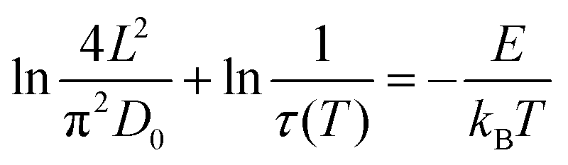 | (3) |
The expression can be further simplified by merging the constants,
 | (4) |
Fig. 3a is a schematic illustration of a biological synapse, and the connection between two adjacent neurons, and this serves as the foundation unit for neural signal transmission in a neural system.29 A schematic demonstration and the working principles of a three-terminal synaptic transistor are illustrated, in which the gate and drain electrodes are utilized to mimic the pre-synapse and post-synapse neuron terminals, respectively.30 For neural activities in a nerve system, when an action potential reaches the presynaptic neuron, the release of neurotransmitters induced by cations takes place in the synaptic cleft. With the diffusion of neurotransmitters to the postsynaptic neuron and then coupling with receptors along the postsynaptic membrane, an action potential is generated and continuously transmitted to the next neuron through axons or dendrites. In explanation of the quantitative connective strength between neurons, synaptic weight is adopted to reveal various event-dependent synaptic plasticities which fundamentally correspond to basic neural activities, memory and learning in the human brain.31 Due to the existence of synapses in neural systems, two opposite kinds of signals, excitatory and inhibitory, are propagated along the signal path through neuron-based networks. A negatively programming pulse and a positively erasing pulse trigger the decrease and increase in drain current of a synaptic transistor, respectively, thus the variations in synaptic weight resemble depression and potentiation synaptic behaviours in biological synapses. We define the increase of postsynaptic current (PSC) amplitude under positive gate pulse as excitatory PSC (EPSC), while the decrease of PSC amplitude under negative gate pulse is regarded as inhibitory PSC (IPSC).
 | ||
| Fig. 3 Synaptic behaviors of BP–ZnO based synaptic transistors. (a) Schematic illustration of a biological synapse. (b) EPSC by applying a single positive presynaptic pulse. (c) PPF behavior by applying two consecutive pulses. (d) 25 cycles for each programming and erasing pulses. (e) Linear synaptic weight control for the realization of 4 weights. (f) Relaxation time (τ) as a function of pulse number. Two forms of STDP, (g) antisymmetric Hebbian learning rule and (h) symmetric anti-Hebbian learning rule. | ||
The BP–ZnO hybrid NP based synaptic transistor is capable of imitating the architecture as well as emulating the functions of a biological synapse. A presynaptic action potential was realized by inputting electrical pulses generated from the gate electrode, while PSC corresponded to the recorded drain–source current.32Fig. 3b gives the response of EPSC of the transistor under the application of a single gate pulse with amplitude of +50 V, width of 10 ms and fixed drain voltage of −30 V.33 It should be noted that a programming gate pulse of −50 V was applied in advance, which ensured that sufficient holes would be trapped in the BP–ZnO hybrid NPs. A read voltage of −30 V was used for emulation of all of the synaptic functions due to the low current response of the erasing process. A sudden increase in current, followed by a smooth current decay was clearly observed, which was attributed to the abrupt accumulation of holes in the pentacene channel and the gradual redistribution of holes to achieve a relatively stable conductance state. The abrupt change in current is consistent with the transfer characteristics of the transistor under erasing bias. However, the decreased current could not reach its initial state within 100 ms, which could be termed as short-term potentiation with a relatively short timescale.
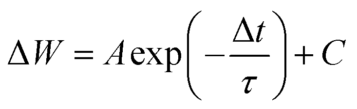
Another significant short-term plasticity PPF, which gives a description of an enhancement in EPSC of the second pulse upon the application of two consecutive presynaptic pulses was further mimicked.34–36 A pair of presynaptic pulses (amplitude = +50 V, width = 10 ms) was applied to the pre-synapse with a relatively short spike interval of 10 ms. As shown in Fig. 3c, the rise in EPSC prompted by the second pulse was obtained. The enhancement could be due to the fact that the back diffusion of trapped holes was not completed before the next spike came in. In order to quantitatively measure the enhancement after the application of the presynaptic pulses to the pre-synapse, the decay curves were fitted by the exponential function shown below:
 | (5) |
Furthermore, we applied consecutive stimuli of gate pulses (amplitude = +50 V, width = 1 s, interval = 0.1 s) as excitatory/inhibitory signals to achieve LTP and LTD. As shown in Fig. 3d, after application of 25 negative/25 positive pulses with a pulse width of 0.5 s and pulse interval of 0.5 s, excellent symmetry was found in the readout current between the two opposite operations, which is considered to be one of the significant issues in evaluating synaptic weight modulation.37 Fig. S6 (ESI†) provides a memory model in which long-term memory (LTM) can be realized by rehearsal of memory events, strongly correlated to the total flux of stimuli input. In this work, we first applied different numbers of presynaptic stimuli (both potentiation and depression) to modulate synaptic weight.16 Before the process of synaptic weight modulation, the initial state of the synaptic transistor was set by applying a negative pulse of −50 V for 5 s. The synaptic weight (ΔW) in the fully negatively programmed state was defined as the “0” level. All readout currents were normalized to the base value (W0) in the form of synaptic weight. A pulse train with fixed pulse parameters (width = 1 s, interval = 1 s, pulse = +50 V) was imposed on the pre-synapse. Fig. 3e demonstrates the different synaptic weights and conductance levels which were well-tuned by the positive/negative electrical pulses. After the employment of 20 pulses, the synaptic weight was increased to about 8% from level “0” to “1”. Then level “2” was implemented by 20 more pulses. Similarly, we successfully achieved a synaptic weight of about 27% to level “3” by applying 20 pulses with the same parameters following the above-mentioned procedure. When we applied 60 pulses of −50 V, the device was then reset to its initial conductance state. Further modulations of the synaptic weight are demonstrated in the right panel of this figure, providing crucial evidence of the linear adjustment of the synaptic weight. The desired synaptic weight of the BP–ZnO hybrid NP synapse was achieved under any unknown situation of synaptic weight by controlling the number of pulses following the reset process. Here, four conductance levels including “3”, “2”, “1” and an initial state “0” have been realized.
LTP behaviours under positive pulse trains with different pulse numbers are shown in Fig. S7 (ESI†).38,39 More applied pulses induce a slower decay process. As summarized in Fig. 3f, evident positive correlation was found between the synaptic weight level and the number of pulses applied.40,41 The experimental data was then fitted with an exponential equation to acquire a time constant of synaptic weight decay, which quantitatively exhibits the prolonged potentiation effect and progress in relaxation time with increased potentiating events.39 The absence of a tunnelling dielectric layer between the semiconductor layer and the BP–ZnO somewhat weakens the ability to realize a long storage lifetime, and gives rise to an ideal matching of the measured results to the exponential equation. The effect on the transistor upon each application of the potentiation pulse train can be neutralized by the counter erasing pulse train. Accordingly, the device can realize LTP within a timescale of hundreds of seconds and possesses the ability to reset itself back to the initial state.
A notable quality in the chemical synapse is the quantification of the number of released neurotransmitters.23 Postsynaptic current is directly linked to the number of released synaptic vesicles, which contain about 104 neurotransmitters. Therefore, PSC is positively correlated with the release probability of neurotransmitters as shown below:23
| PSC ∝ PRNTf(NAP) | (6) |
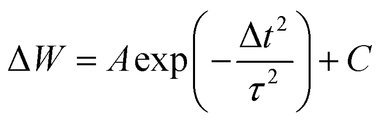
In biological synapses, STDP is one of the most significant Hebbian learning rules that is highly related to the temporal order and interval (Δt) of pre- and postsynaptic spikes.44–46 With precise timing control, synaptic weight can be modulated in both magnitude and polarity. For antisymmetric Hebbian learning, if the pre-synaptic spike arrives ahead of the post-synaptic spike (Δt > 0), the synaptic weigh would be reinforced, and this process is termed LTP. In contrast, LTD occurs if the post-synaptic spike precedes the pre-synaptic spike (Δt < 0), leading to a decrease in the connection strength between two adjacent neurons.47,48 A shorter time interval between two spikes induces a greater response in synaptic weight. Here, we performed two forms of STDP learning rules (antisymmetric Hebbian and symmetric anti-Hebbian learning rules) as representative examples, during which the gate and drain electrodes acted as pre- and post-synapses, respectively. The synaptic weight was employed to quantify the long-term potentiation and depression processes with respect to the time interval for the antisymmetric Hebbian learning rule, as shown in Fig. 3g, and the experimental results can be well fitted as the exponential form:49,50
 | (7) |
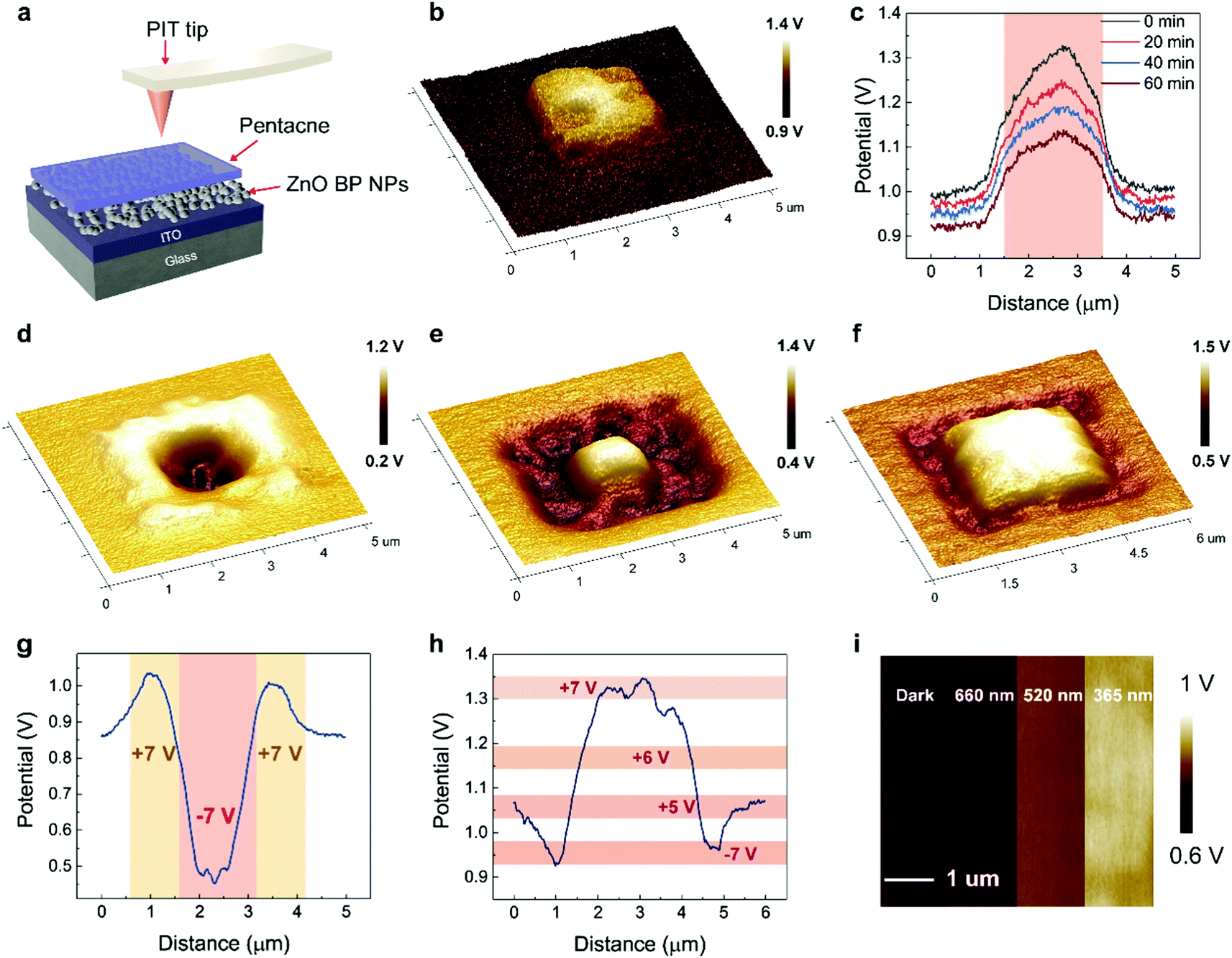
Besides, for the symmetric anti-Hebbian learning rule as shown in Fig. 3h, depression effects occur for all of the time intervals (Δt). Therefore, in this case, the variation in synaptic weight solely depends on the interval between two spikes, and not on the temporal order. Furthermore, the experimental results corresponding to the symmetric anti-Hebbian learning rule can be expressed as a Gaussian function:49
 | (8) |
The highly controllable photo-induced carrier concentration in the BP–ZnO hybrid NPs indicates the possibility of controlling the synaptic weight with photon pulses, which would be beneficial for wideband optical communication protocols. A train of pulses including 40 consecutive pulse stimuli with fixed pulse parameters with a pulse width of 100 ms, and an interval of 100 ms were applied (amplitudes of pulse and base values were +50 V and −30 V, respectively). During these measurements, green, red and UV light sources with wavelengths of 660, 520 and 365 nm were employed at a fixed intensity of 150 mW cm−2 along with an electrical input to act as an additional presynaptic input while the operation under dark conditions acted as the control group. The original data for these four operations, shown in Fig. 4a, shows a much higher current under green and red illumination than that under UV or dark conditions. Besides, Fig. 4b demonstrates the synaptic weight change after the application of the pulse train, which indicates that the application of different light sources not only increases the response current, but also facilitates the enhancement in synaptic weight change during the 40 pulses.
 | ||
| Fig. 4 (a) Readout peak current of 40 consecutive positive pulses (width = 0.1 s, interval = 0.1 s) with different light illumination. (b) Calculated synaptic weight in (a). 10 consecutive positive pulses (width = 5 s, interval = 5 s) under green, red light (c), and UV (d) compared with a dark control group. (e) Calculated synaptic weights in (c) and (d). The inset in (e) demonstrates the calculated PTP and PPF index. (f) Readout current upon different durations of UV illumination. (g) Peak value of readout PSC of 10 consecutive postsynaptic pulses with constant presynaptic pulse. | ||
Another pulse train with a pulse duration of 5 s (interval = 5 s) for 10 consecutive waveforms was applied to the pre-synapse to provide a more explicit description of the effect of optical programming on the synaptic weight. The results under green/red illumination and UV are depicted in Fig. 4c and d, respectively. The response currents under green/red light illumination quickly reached a saturated state due to the increase in the amount of free charge carriers inside the pentacene. This phenomenon is quite consistent with the intrinsic characteristics of biological synapses, since the postsynaptic response becomes saturated if the intensity of the stimuli input is sufficiently applied. On the contrary, the response current in Fig. 4e reveals linear synaptic modulation of synaptic weight under both dark conditions and UV illumination without a saturated state during the application of 10 pulses, indicating a well-regulated synaptic weight.51 As we mentioned above, red and green light is mainly absorbed by pentacene which instantaneously generates a number of charge carriers resulting in a sudden increase in IDS. Nevertheless, most of the UV irradiation passes through the semiconductor layer and is absorbed by the BP–ZnO hybrid NPs. Newly generated electron–hole pairs are immediately separated, followed by the flow of holes towards the pentacene through the energy band bending and positive external electric field. Under the application of periodic positive pulses, the current in the channel will gradually increase instead of quickly reaching its saturated state. The current in the first readout state is defined as the I0, and the readout current at the nth pulse is termed as In upon the application of electrical pulses. Here, we define a PPF index: PPF = (I2 − I1)/I1 × 100% as well as a PTP index: PTP = (I5 − I1)/I1 × 100% to systematically investigate the modulation of synaptic weight since linear regulation of synaptic events is of vital importance (inset in Fig. 4e).36,52 Analogous results were obtained from 10 other devices to confirm the above characteristics.
Fig. 4f demonstrates the operating sequence and readout PSC of the BP–ZnO hybrid NP device. The device was reset to the initial state prior to exposure under a light pulse. The synaptic transistor was irradiated with UV illumination with a duration ranging from 1 s to 3 s while leaving a 1 s gap without illumination away from the arrival of a postsynaptic pulse.53 The presynaptic stimulus was fixed as constant at −30 V. It is worth noting that the amplitude of the postsynaptic stimulus was set to be −30 V. The readout current under each light illumination was smaller than that in the dark conditions. As the duration of light illumination increased, the readout current decreased, which revealed a light-assisted depression effect. This phenomenon can be explained as the strengthened screening effect from the BP–ZnO hybrid NP layer due to the generation and accumulation of light-induced holes, and thus a decrease of the readout current. For the sake of enlarging the weakening effect of the readout PSC, an extracted peak value of each readout PSC under light illumination was plotted as a function of stimulus spike as illustrated in Fig. 4g. A control group was set up by the combination of a constantly imposed gate bias of −30 V and a drain pulse with an amplitude of −3 V which would not affect the synaptic behaviour. The readout current decreased a little owing to the small electric field. With the introduction of light illumination, a decreased trend was obviously captured with an increased attenuation rate though the PSC that was much higher under red and green light illumination. It is easy to augment the channel conductance by simply illuminating the semiconductor with light that matches its absorption. Therefore, combined with our above obtained results, we proposed a feasible photoactive synapse endowed with bi-directional tunability over a relatively broadband range. It should be noted that our synaptic transistor can be effectively controlled by light illumination with a fixed light intensity. The number of applied light pulses was not changed for the purpose of a cost-effective and easy illumination process as well as avoiding any further efforts to modulate light intensity. Besides, the duration of applied light pulses was also fixed during the measurements. The characterization results with the application of light illumination displayed an excellent response to optical stimuli since the BP–ZnO hybrid NPs possessed superior properties of enhanced photon harvesting as well as fast exciton separation, which led to the excellent performance of our fabricated photoactive synaptic transistor. On the other hand, the BP QDs inside the hybrid NPs were protected from the ambient environment due to the oriented packing of the ZnO NPs. The BP–ZnO NP-based synaptic transistor displayed inevitable fluctuations in synaptic performance for more than one month, indicating excellent stability in ambient conditions.24,54
To elucidate the operation principles of the transport of charge carriers inside the synaptic transistor, in situ KPFM was performed with a platinum/iridium-coated conductive tip as schematically depicted in Fig. 5a. It should be underlined that the AFM measurements were conducted on a spin-coated thin film of BP–ZnO NPs. The AFM was first switched to the contact mode to perform a 2 μm × 2 μm square area scan with a tip bias of +7 V. Then the contact potential difference (CPD) on a 5 μm × 5 μm area between the conductive tip and the ZnO–phosphorene hybrid NP layer was monitored in the KPFM mode as shown in Fig. 5b.55,56 The images were captured to track the variation in potential (Fig. 5c). Over time, trapped holes exhibited gradual relaxation, indicating a potential recovery to the initial state, which is consistent with our previous device level results. Since charge trapping plays an important role during the whole electrical synaptic measurement of our BP–ZnO based synaptic transistor, both electron and hole injections were carried out in the electrical AFM measurements. Stored charge carriers were characterized in the form of surface potential. We first performed a scan within an area of 3 μm × 3 μm by applying +7 V on the conductive tip. Holes could be injected from the positively charged conductive tip into the BP–ZnO hybrid NP film, corresponding to the yellow region in the image. In the following process, a smaller 1 μm × 1 μm area in the centre was scanned by applying a −7 V tip bias. After the application of the negative bias, the trapped holes recombined with newly injected electrons, while leaving a deeply trapped electron trapping state. Fig. 5d demonstrates a typical three-dimensional KPFM image of electron trapping sites surrounded by hole trapping sites. The yellow region is considered to be a hole trapping state and dark region correspond to an electron trapping state. Surface potential data retrieved from Fig. 5d along a straight line in the centre is depicted in Fig. 5g. The potential difference between the two trapping states was found to be about 600 mV, producing the “volcano” like image. Conversely, a tip bias with reverse polarity was applied and the inverse scanned image is shown in Fig. 5e to further confirm the bipolar charge carrier trapping of the BP–ZnO hybrid NP film, and therefore an enhanced synaptic efficacy can be achieved with a variety of synaptic functions. Similar to the realization of 4 conductance levels as we mentioned before, here, we also implemented different levels of incremental surface potential by the application of various tip biases including −7 V, + 5 V, +6 V and +7 V among the diminishing square areas, as shown in Fig. S10 (ESI†). Accordingly, as exhibited in Fig. 5f, the KPFM results obtained from the charge trapping operations support our hypothesis that the photoactive synaptic behaviour of our device originates from the charge trapping ability of the BP–ZnO hybrid NP layer, while Fig. 5h provides the line profiles. Fig. 5i shows the surface potential of the BP–ZnO hybrid NP film after light illumination at various wavelengths ranging from 660 nm to 365 nm with a fixed intensity of 150 mW cm−2. As displayed in this figure, the surface potential steadily increases when the wavelength of light illumination is fixed at 660, 520 and 365 nm, respectively. In general, the increase in surface potential originates from the accumulation of holes and reduction of electrons generated by light illumination. As mentioned before, light illumination on the BP–ZnO hybrid NP film can trigger the generation of photo-carriers. The photogenerated electron–hole pairs can easily be separated and holes are driven from the BP–ZnO hybrid NPs to the pentacene layer through energy band bending and an external electric field. The photo-induced electrons trapped in the BP–ZnO hybrid NPs induces an abrupt increase of the surface potential. The largest increased surface potential under 365 nm is consistent with the strongest synaptic weight modulation capability of UV light.
 | ||
| Fig. 5 KPFM measurement of deposited BP–ZnO hybrid NP thin film and pentacene. (a) Schematic diagram of the KPFM operation. (b) Image of three-dimensional surface potential within a 5 μm × 5 μm area, where the bump area (5 μm × 5 μm) was pre-applied with +7 V. (c) Data of surface potential derived from images captured over 60 min to explore the trapping properties. (d) Image of three-dimensional surface potential within a 5 μm × 5 μm area. We first applied +7 V to the 3 μm × 3 μm area, followed by an application of −7 V to a 1 μm × 1 μm area. (e) Image of three-dimensional surface potential within a 5 μm × 5 μm area. We first applied −7 V to the 3 μm × 3 μm area, followed by an application of +7 V to a 1 μm × 1 μm area. (f) Realization of different levels of surface potentials by applying tip biases with various amplitudes and polarities. (g) Line profiles of potential change in (c) along a straight line across the centre. (h) Line profiles of potential change in (f) along a straight line across the centre. (i) Surface potential of the pentacene film for the device with illumination of light of different wavelengths. | ||
In this article, we have presented a novel approach to systematically modulate the synaptic weight of a synaptic transistor via both electrical and optical inputs on a SiO2/Si substrate to realize linear modulation, while the relatively large operation voltage and power consumption can be optimized by replacing the gate dielectric with metal oxides such as Al2O3. Here, we mainly focused on the feasibility of electrical tuning and the introduction of an external light stimuli as presynaptic inputs.
4. Conclusions
In summary, extensive synaptic weight modulation was shown for the first time in a BP–ZnO hybrid NP-based transistor by combining both electronic mode and photoactive mode operation. The electronically modulated charge trapping inside the thin BP–ZnO NPs ensured an enlargement in the variation margin while optical control of the excitatory and inhibitory synaptic weight with symmetry and linearity variation was further realized due to the extended energy threshold of photon absorption and accelerated dissipation of excitons in the BP–ZnO NPs. Owing to the excellent broadband response of the hybrid NPs, multiple forms of synaptic plasticity can be achieved by readily exposing the device to light of different wavelengths. Compared to previously reported synaptic devices, such photoactive synapses with metaplasticity effects pave the way for multifunctional neuromorphic computing systems with rapid signal propagation and photosensing purposes which may potentially ease network level concerns.Conflicts of interest
There are no conflicts to declare.Acknowledgements
The authors acknowledge grants from the Natural Science Foundation of China (Grant No. 61604097 and 61601305), the Science and Technology Innovation Commission of Shenzhen (Grant No. JCYJ20170818143618288, JCYJ20170302145229928, JCYJ20170302151653768 and ZDSYS201707271554071), Shenzhen Peacock Technological Innovation Project (Grant No. KQJSCX20170727100433270 and KQJSCX20170327150812967), Guangdong Provincial Department of Science and Technology (Grant No. 2017TQ04X082, 2018B030306028 and 2017A010103026), the Department of Education of Guangdong Province (Grant No. 2016KTSCX120), and the Natural Science Foundation of SZU.Notes and references
- H. S. Wong and S. Salahuddin, Nat. Nanotechnol., 2015, 10, 191–194 CrossRef CAS PubMed.
- J. J. Yang, D. B. Strukov and D. R. Stewart, Nat. Nanotechnol., 2013, 8, 13–24 CrossRef CAS.
- M. Prezioso, F. Merrikh-Bayat, B. D. Hoskins, G. C. Adam, K. K. Likharev and D. B. Strukov, Nature, 2015, 521, 61–64 CrossRef CAS.
- J. Von Neumann, IEEE Ann. Hist. Comput., 1988, 10, 243–256 Search PubMed.
- D. Kuzum, S. Yu and H. S. Wong, Nanotechnology, 2013, 24, 382001 CrossRef PubMed.
- J. von Neumann and R. Kurzweil, The Computer and the Brain, Yale Univ. Press, 2012 Search PubMed.
- L. Sun, Y. Zhang, G. Hwang, J. Jiang, D. Kim, Y. A. Eshete, R. Zhao and H. Yang, Nano Lett., 2018, 18, 3229–3234 CrossRef CAS.
- Y. van de Burgt, A. Melianas, S. T. Keene, G. Malliaras and A. Salleo, Nat. Electron., 2018, 1, 386–397 CrossRef.
- Z. Wang, L. Wang, M. Nagai, L. Xie, M. Yi and W. Huang, Adv. Electron. Mater., 2017, 3, 1600510 CrossRef.
- M. A. Zidan, J. P. Strachan and W. D. Lu, Nat. Electron., 2018, 1, 22–29 CrossRef.
- S. H. Jo, T. Chang, I. Ebong, B. B. Bhadviya, P. Mazumder and W. Lu, Nano Lett., 2010, 10, 1297–1301 CrossRef CAS.
- D. Ielmini and H. S. P. Wong, Nat. Electron., 2018, 1, 333–343 CrossRef.
- D. S. Jeong and C. S. Hwang, Adv. Mater., 2018, 1704729, DOI:10.1002/adma.201704729.
- B. Gao, Y. Bi, H.-Y. Chen, R. Liu, P. Huang, B. Chen, L. Liu, X. Liu, S. Yu, H. S. P. Wong and J. Kang, ACS Nano, 2014, 8, 6998–7004 CrossRef CAS PubMed.
- M. Qi, L. Bai, H. Xu, Z. Wang, Z. Kang, X. Zhao, W. Liu, J. Ma and Y. Liu, J. Mater. Chem. C, 2018, 6, 2026–2033 RSC.
- Z. Cheng, C. Ríos, W. H. P. Pernice, C. D. Wright and H. Bhaskaran, Sci. Adv., 2017, 3, 1700160 CrossRef.
- S.-T. Han, Y. Zhou and V. A. L. Roy, Adv. Mater., 2013, 25, 5425–5449 CrossRef CAS PubMed.
- J. Lee and W. D. Lu, Adv. Mater., 2018, 30, 1702770 CrossRef PubMed.
- L. Q. Zhu, C. J. Wan, L. Q. Guo, Y. Shi and Q. Wan, Nat. Commun., 2014, 5, 3158 CrossRef PubMed.
- C. Liu, X. Yan, X. Song, S. Ding, D. W. Zhang and P. Zhou, Nat. Nanotechnol., 2018, 13, 404–410 CrossRef CAS.
- J. Zhu, Y. Yang, R. Jia, Z. Liang, W. Zhu, Z. U. Rehman, L. Bao, X. Zhang, Y. Cai, L. Song and R. Huang, Adv. Mater., 2018, 30, 1800195 CrossRef.
- T. V. P. Bliss and G. L. Collingridge, Nature, 1993, 361, 31 CrossRef CAS.
- A. J. Arnold, A. Razavieh, J. R. Nasr, D. S. Schulman, C. M. Eichfeld and S. Das, ACS Nano, 2017, 11, 3110–3118 CrossRef CAS PubMed.
- L. Hu, J. Yuan, Y. Ren, Y. Wang, J. Q. Yang, Y. Zhou, Y. J. Zeng, S. T. Han and S. Ruan, Adv. Mater., 2018, 30, 1801232 CrossRef.
- L. Zhou, J. Mao, Y. Ren, S. T. Han, V. A. L. Roy and Y. Zhou, Small, 2018, 14, 1703126 CrossRef.
- Z. Q. Wang, H. Y. Xu, X. H. Li, H. Yu, Y. C. Liu and X. J. Zhu, Adv. Funct. Mater., 2012, 22, 2759–2765 CrossRef CAS.
- Y. B. Nian, J. Strozier, N. J. Wu, X. Chen and A. Ignatiev, Phys. Rev. Lett., 2007, 98, 146403 CrossRef CAS.
- H. Tian, Q. Guo, Y. Xie, H. Zhao, C. Li, J. J. Cha, F. Xia and H. Wang, Adv. Mater., 2016, 28, 4991–4997 CrossRef CAS.
- B. Li, Y. Liu, C. Wan, Z. Liu, M. Wang, D. Qi, J. Yu, P. Cai, M. Xiao, Y. Zeng and X. Chen, Adv. Mater., 2018, 30, 1706395 CrossRef PubMed.
- Q. Lai, L. Zhang, Z. Li, W. F. Stickle, R. S. Williams and Y. Chen, Adv. Mater., 2010, 22, 2448–2453 CrossRef CAS.
- H. Tian, W. Mi, H. Zhao, M. A. Mohammad, Y. Yang, P. W. Chiu and T. L. Ren, Nanoscale, 2017, 9, 9275–9283 RSC.
- C. J. Wan, L. Q. Zhu, Y. H. Liu, P. Feng, Z. P. Liu, H. L. Cao, P. Xiao, Y. Shi and Q. Wan, Adv. Mater., 2016, 28, 3557–3563 CrossRef CAS PubMed.
- R. A. John, J. Ko, M. R. Kulkarni, N. Tiwari, N. A. Chien, N. G. Ing, W. L. Leong and N. Mathews, Small, 2017, 13, 1701193 CrossRef.
- L. Zhou, J. Y. Mao, Y. Ren, J. Q. Yang, S. R. Zhang, Y. Zhou, Q. Liao, Y. J. Zeng, H. Shan, Z. Xu, J. Fu, Y. Wang, X. Chen, Z. Lv, S. T. Han and V. A. L. Roy, Small, 2018, 14, 1800288 CrossRef.
- F. Yu, L. Q. Zhu, W. T. Gao, Y. M. Fu, H. Xiao, J. Tao and J. M. Zhou, ACS Appl. Mater. Interfaces, 2018, 10, 16881–16886 CrossRef CAS.
- J. Jiang, J. Guo, X. Wan, Y. Yang, H. Xie, D. Niu, J. Yang, J. He, Y. Gao and Q. Wan, Small, 2017, 13, 1700933 CrossRef.
- Y. van de Burgt, E. Lubberman, E. J. Fuller, S. T. Keene, G. C. Faria, S. Agarwal, M. J. Marinella, A. Alec Talin and A. Salleo, Nat. Mater., 2017, 16, 414–418 CrossRef CAS.
- T. Chang, S.-H. Jo and W. Lu, ACS Nano, 2011, 5, 7669–7676 CrossRef CAS PubMed.
- T. Ohno, T. Hasegawa, T. Tsuruoka, K. Terabe, J. K. Gimzewski and M. Aono, Nat. Mater., 2011, 10, 591–595 CrossRef CAS PubMed.
- Y. Park and J. S. Lee, ACS Nano, 2017, 11, 8962–8969 CrossRef CAS PubMed.
- M. K. Kim and J. S. Lee, ACS Nano, 2018, 12, 1680–1687 CrossRef CAS PubMed.
- S. Kim, C. Du, P. Sheridan, W. Ma, S. Choi and W. D. Lu, Nano Lett., 2015, 15, 2203–2211 CrossRef CAS PubMed.
- Z. Wang, S. Joshi, S. E. Savel'ev, H. Jiang, R. Midya, P. Lin, M. Hu, N. Ge, J. P. Strachan, Z. Li, Q. Wu, M. Barnell, G. L. Li, H. L. Xin, R. S. Williams, Q. Xia and J. J. Yang, Nat. Mater., 2017, 16, 101–108 CrossRef CAS PubMed.
- Z. Xiao and J. Huang, Adv. Electron. Mater., 2016, 2, 1600100 CrossRef.
- Z. H. Tan, R. Yang, K. Terabe, X. B. Yin, X. D. Zhang and X. Guo, Adv. Mater., 2016, 28, 377–384 CrossRef CAS PubMed.
- R. Yang, H.-M. Huang, Q.-H. Hong, X.-B. Yin, Z.-H. Tan, T. Shi, Y.-X. Zhou, X.-S. Miao, X.-P. Wang, S.-B. Mi, C.-L. Jia and X. Guo, Adv. Funct. Mater., 2018, 28, 1704455 CrossRef.
- X. Yan, J. Zhao, S. Liu, Z. Zhou, Q. Liu, J. Chen and X. Y. Liu, Adv. Funct. Mater., 2018, 28, 1705320 CrossRef.
- J. Yin, F. Zeng, Q. Wan, F. Li, Y. Sun, Y. Hu, J. Liu, G. Li and F. Pan, Adv. Funct. Mater., 2018, 28, 1706927 CrossRef.
- Y. Li, Y. Zhong, L. Xu, J. Zhang, X. Xu, H. Sun and X. Miao, Sci. Rep., 2013, 3, 1619 CrossRef PubMed.
- Y. Li, Y. Zhong, J. Zhang, L. Xu, Q. Wang, H. Sun, H. Tong, X. Cheng and X. Miao, Sci. Rep., 2014, 4, 4906 CrossRef CAS.
- M. Kumar, D.-K. Ban and J. Kim, Mater. Lett., 2018, 225, 46–49 CrossRef CAS.
- C. S. Yang, D. S. Shang, N. Liu, G. Shi, X. Shen, R. C. Yu, Y. Q. Li and Y. Sun, Adv. Mater., 2017, 29, 1700906 CrossRef.
- J. Lee, S. Pak, Y. W. Lee, Y. Cho, J. Hong, P. Giraud, H. S. Shin, S. M. Morris, J. I. Sohn, S. Cha and J. M. Kim, Nat. Commun., 2017, 8, 14734 CrossRef CAS PubMed.
- S. T. Han, L. Hu, X. Wang, Y. Zhou, Y. J. Zeng, S. Ruan, C. Pan and Z. Peng, Adv. Sci., 2017, 4, 1600435 CrossRef.
- C. Yoon, J. H. Lee, S. Lee, J. H. Jeon, J. T. Jang, D. H. Kim, Y. H. Kim and B. H. Park, Nano Lett., 2017, 17, 1949–1955 CrossRef CAS.
- Y. Sharma, J. Balachandran, C. Sohn, J. T. Krogel, P. Ganesh, L. Collins, A. V. Ievlev, Q. Li, X. Gao, N. Balke, O. S. Ovchinnikova, S. V. Kalinin, O. Heinonen and H. N. Lee, ACS Nano, 2018, 12, 7159–7166 CrossRef CAS.
Footnote |
| † Electronic supplementary information (ESI) available. See DOI: 10.1039/c8tc05030a |
| This journal is © The Royal Society of Chemistry 2019 |