
 Open Access Article
 This Open Access Article is licensed under a Creative Commons Attribution-Non Commercial 3.0 Unported Licence
Hot carrier solar cells and the potential of perovskites for breaking the Shockley–Queisser limit
Simon
Kahmann
 and
Maria A.
Loi
*
and
Maria A.
Loi
*
University of Groningen, Nijenborgh 4, 9747AG Groningen, The Netherlands. E-mail: m.a.loi@rug.nl
First published on 6th February 2019
Abstract
In this review article, we discuss the working mechanism of hot carrier solar cells (HCSCs), their prerequisites from a material point of view and consider power conversion efficiencies that could reasonably be achieved with these devices. We review phonon decay pathways and proposed design rules for hot carrier absorbers established for classical bulk materials, as well as engineering efforts based on nanostructuring. Our main focus, however, lies on the recently emerged class of metal halide perovskites that not only exhibits tremendous potential in standard solar cells, but also offers highly promising hot carrier lifetimes. We discuss possible origins for this encouraging observation and point out pathways for future research towards HCSCs that break the Shockley–Queisser limit.
 Simon Kahmann | Simon Kahmann has been a research fellow in the group of Maria A. Loi since 2018. He received a shared doctorate degree from the University of Groningen, The Netherlands and the Friedrich-Alexander University Erlangen-Nuremberg (FAU), Germany in 2018. During his studies, he worked on nanomaterials for opto-electronic applications in the group of Prof. Maria A. Loi and the Institute for Materials in Electronics and Energy Technology of Prof. Christoph J. Brabec. Before, he received a bachelor's degree in Microtechnology from the University of Applied Sciences in Zwickau, Germany in 2011, followed by a master's degree in Nanotechnology from the FAU, which involved studies at the University of Linköping, Sweden. |
 Maria A. Loi | Maria Antonietta Loi studied physics at the University of Cagliari in Italy, where she received her PhD in 2001. In the same year, she joined the Linz Institute for Organic Solar Cells at the University of Linz in Austria as a postdoctoral fellow. Later, she worked as researcher at the Institute for Nanostructured Materials of the Italian National Research Council in Bologna, Italy. In 2006, she became Assistant Professor and Rosalind Franklin Fellow at the Zernike Institute for Advanced Materials of the University of Groningen in The Netherlands. Since 2014, she has been full professor in the same institution and chair of the Photophysics and OptoElectronics group. |
Although there are many important factors that determine whether a device is a viable candidate for large-scale photovoltaic production (amongst them the stability, energy consumption during production, material costs and toxicity), the first parameter most researchers look for is the power conversion efficiency (PCE). The PCE for relevant single junction technologies lies between 10 and 30% with quantum dot and organic solar cells on the lower end and gallium arsenide cells on the upper end of this range.1 An upper limit of the theoretically achievable PCE with a material system can be found through the theory of Shockley and Queisser (SQ).2
This maximum PCE is predominantly governed by the band gap energy of the absorber material, since photons with lower energy cannot be absorbed (therefore they do not contribute to the device photocurrent) and charge carriers excited by photons with energy exceeding the band gap lose a big portion of this energy due to heat dissipation.3 For a single junction solar cell, this leads to a maximum PCE of 33.7% for the optimal band gap of 1.34 eV under 1 sun illumination – a value that increases to approximately 41% for maximum solar concentration (46![[thin space (1/6-em)]](https://www.rsc.org/images/entities/char_2009.gif) 200 suns).4
200 suns).4
1 Hot carrier solar cells to exceed the Shockley–Queisser limit
Several approaches have been proposed to overcome this limit and thereby make photovoltaics an even more attractive technology as a future sustainable energy source.5 Most of these efforts focus on increasing the number of extracted charges (i.e. increasing the device current), for example by using several sub band gap energy photons to generate one photon above the gap (up-conversion) or to use one high energy photon to generate several charge carriers (multiple exciton generation, singlet exciton fission).6,7Reducing the losses due to carrier relaxation (thus increasing the device voltage) could be achieved through the use of several junctions, i.e. a cascade of absorber materials with progressively narrower band gaps. Such so-called tandem or multijunction cells significantly increase the PCE, but require a more complex device architecture.
In single junction solar cells, the excess energy of these photons could be harvested by extracting charge carriers before relaxation – a concept called hot carrier solar cell (HCSC). This idea was already proposed in 1982 and said to improve the maximum PCE to 66% under 1 sun illumination and approximately 85% for maximum solar light concentration.8 Compared with tandem devices, HCSCs were furthermore shown to be less sensitive to variations of the illumination spectrum (as e.g. occurring through different angles of sunlight incidence during the day).9
Strikingly, though, experimental work to realise this concept is scarce. This is due to two big challenges. The first one is to find a suitable absorber material, in which cooling is slowed down to allow for the extraction of carriers with excess energy, whilst still having all the characteristics of a good solar cell material, namely, a strong absorption over a broad spectral range and a favourable charge transport. The second challenge is to engineer contact materials (ideally) with a narrow density of states at an appropriate energy level (energy selective contacts, ESCs) to suppress the cooling through the contacts and leakage of hot carriers.10 Besides a significant number of studies enquiring into the realistically achievable PCE in HCSCs, experimental work in this field generally addresses either of these challenges.
In this review, we discuss the working mechanism of HCSCs with a focus on the absorber layer. We discuss the pathways of carrier relaxation as well as approaches to improve desired properties. We account for so-far considered material classes and consider the benefits of nanostructures, but especially focus on the new class of metal halide perovskites (HaPs) and consider reasons why these materials show such promising behaviour. A brief insight is also given into the second big challenge: the energy selective contacts.
2 Solar cell design principles and practical limits
Before reviewing the materials science aspects necessary to keep charge carriers from cooling down and lose their excess energy, we briefly introduce the concept of a hot carrier solar cell. Our discussion follows the device architecture proposed by Würfel, shown in Fig. 1. For interesting alternative concepts, such as optical selective contacts, intermediate band devices or hot carrier extraction via plasmonics, we refer the interested reader to the literature.12–14 The architecture in Fig. 1 is largely analogous to conventional solar cells, with an absorber layer sandwiched between two electrical extracting layers and a pair of external electrodes. The extracting contacts act as membranes with a narrow width δE to extract hot electrons at energy Ee and hot holes at Eh from the absorber. This is necessary because interaction of hot carriers with the lattice if the outside electrode is unavoidable during carrier extraction. This leads to a rapid cooling of the carriers from Te/Th to the electrode lattice temperature TL (assumed to be identical to the absorber temperature), which is accompanied by entropy generation in classical device architectures. The entropy is transferred to the electrode lattice and is lost for the carriers. Simultaneously, cold carriers from the electrode could be injected into the absorber and thereby reduce the energy of the hot carrier population. Due to the narrow band of allowed states (δE < kBTL), hot carriers in ESCs cannot relax to lower states. They hence cool down isentropically to TL whilst producing chemical energy by increasing the separation of the quasi Fermi-energies μce and μch in the contacts (μceh).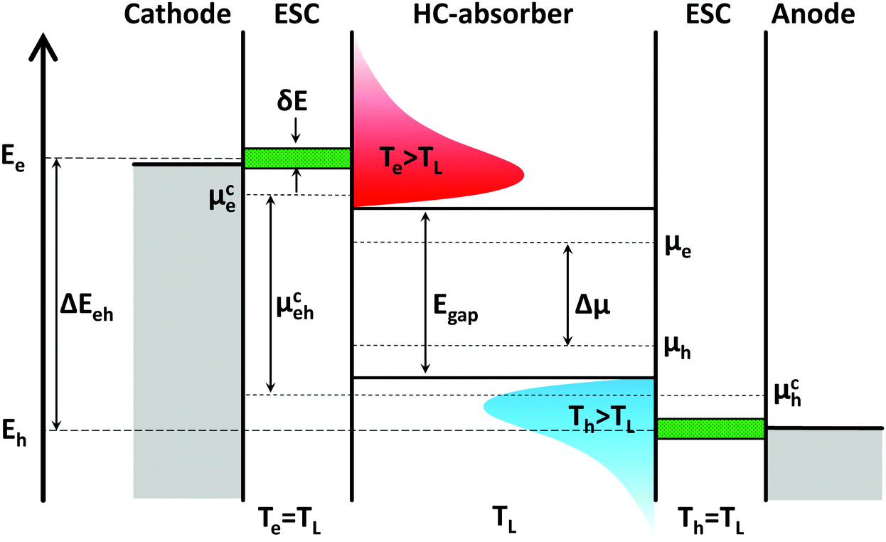 | ||
| Fig. 1 The proposed scheme of a hot carrier solar cell working under non-equilibrium conditions involves an absorber layer in which charge carriers cool only slowly towards the lattice temperature TL. The extraction of such hot carriers occurs through energetically narrow selective contacts (ESCs, green) to isentropically cool down the carriers. This process allows to generate a larger splitting of the quasi-Fermi levels or a higher chemical potential μehc than under equilibrium conditions.11 In the latter case, the chemical potential Δμ is limited by the absorber band gap Egap. | ||
The open circuit voltage of such a device, assuming an identical hot carrier temperature Teh and a separation ΔEeh of the ESCs, is then given by:
 | (1) |
The short circuit current, in the ideal case, is governed by the difference in absorbed and emitted photons (radiative limit). These are determined by the band gap of the absorber Egap. Assuming full absorption of photons with energy Eph > Egap, the maximum efficiency of 66% under 1 sun illumination is found for a band gap of around 0.7 to 0.9 eV. Under maximum concentration, with above mentioned predicted PCE of 85%, the ideal band gap would be equal to zero, since the increase in harvested photons for reducing the band gap exceeds the accompanying loss in recombination current.11,16
Both initial discussions by Ross and Nozik8 and Würfel11 considered the maximum thermodynamically achievable efficiency, i.e. in absence of carrier relaxation. In such idealised cases, energy dissipation from the absorber only takes place through light emission. This is far from realistic. The most critical aspects are (i) the relaxation time τre that governs the carrier cooling and (ii) the width δE of the ESC, that governs heat dissipation due to entropy generation by the carrier flux into the electrode. In the following, we shall discuss some of the main considerations leading to lower PCEs in real devices and what needs to be taken into account for proper modelling. We focus on the main concepts rather than detailing reported values and refer to a great overview of the latter in the literature.17
It was repeatedly shown that the carrier relaxation time has the largest impact on the efficiency.18,19 For a meaningful contribution of hot carriers, τre needs to be on the time scale of radiative recombination. Based on the broad literature, a PCE of around 50% seems to be reachable if a relaxation time of 1 ns can be achieved. Alternative to τre, heat dissipation can also be discussed through the thermalisation rate Qth,19 which for bulk GaAs was found to be 1000 W K−1 cm−2 and for GaSb-based quantum wells approximately 50 W K−1 cm−2.20 Ultimately, values lower than 1 W K−1 cm−2 seem to be necessary for significant hot-carrier contributions.9,20
Additional to the relaxation time, two more time scales have a major effect on the performance of HCSCs.21 Firstly, the carrier equilibration (or thermalisation) time τeq is a measure for the rate with which an equilibrium carrier distribution (at elevated temperature) is established. Since the ESCs extract carriers only within a narrow energy range at Ee and Eh, these levels could quickly deplete and limit the extractable current. A short τeq serves to repopulate this level and should be at least 1000 times faster than carrier relaxation.21
Secondly, the carrier extraction time τex (also called retention time) describes the duration of carrier presence in the absorber. On first glance, a short time seems desired to minimise relaxation losses, but rapid extraction will also reduce the carrier concentration within the absorber. The carrier concentration has a big impact on the device efficiency through the carrier temperature Teh (consider eqn (1)). In an extensive investigation into the role of the carrier concentration, it was found that for maximum performance τex should be around 1/10 of τre.18 Analogously, light concentration as a means to increase the carrier concentration in the absorber plays a major role for increased PCE. When operating merely under 1 sun, the maximum PCE for realistic parameters, e.g. δE = 0.1 eV and τre = 100–1000 ps is expected to remain below 40%.21 As a clarification, we would like to point out that these timescales used in modelling are not constant material properties, but in reality depend on the carrier energy and concentration.
The second aspect involves the properties of the ESCs. The energetic positions of the ESCs (Ee, Eh) were shown to be best adjusted to the average energy of the hot charge carriers. Whilst carriers at higher energy then cannot be extracted, they can successively re-equilibrate (thermalise) and occupy the extraction level. Ideally, this includes a transfer of energy to carriers below Ee (above Eh) that successively allows for their extraction.22
So far, the discussion assumed an ideally narrow δE of the ESCs. This way, thermal energy loss towards the contacts through carrier extraction is impossible. For real systems, δE has a finite width and heat loss is unavoidable. For a width of around kBTL, the heat loss was shown to amount to around 10% of the incident power (assuming full concentration).19 At a width of 1 eV, this increases to about 20% of the incident power. Although this seems like a big drawback, this is a promising message for device manufacturing, as it allows for considering semi-selective contacts (i.e. a potential step at Ee/Eh) to achieve an improvement in efficiency over classical devices (up to 50% PCE19). Compared to classical devices, such a solar cell would essentially generate a larger voltage due to the thermoelectric contribution (eqn (1)).15
2.1 Energy selective contacts
Würfel assumed an ideal extraction of hot carriers from the absorber and proposed a wide band gap material with narrow conduction/valence band as a candidate, but more recent ideas focussed on the application of quantum well (QW) or quantum dot (QD) nanostructures to reduce entropy losses. Given that QDs act as real energy selective contacts and QWs merely as potential steps, a larger maximum PCE for QD based ESCs is commonly expected.23,24 Furthermore, these two concepts will give rise to different optimal extraction levels and there seems to be an optimum of the contact's conductance. Whilst an inferior PCE at low conductances is readily explainable through increased relaxation losses, a large conductance is predicted to deplete the carrier concentration in the absorber more than necessary (the effect is equal to a small retention time, see above).23The generally proposed design for QD containing ESCs is a double barrier resonant tunnelling contact (DBRT), wherein the QDs are either sandwiched between two wide band gap insulators or embedded in a wide band gap matrix. Reported systems include silicon quantum dots embedded in a SiO2 matrix,25 or between ultrathin Al2O3 (see Fig. 2),26 and PbS QDs sandwiched between Al2O3 barriers (δE = 30–40 meV at RT).27 Importantly, hot carrier extraction through a non-epitaxial double barrier resonant structure was shown for Si QDs even from a poorly suited Si wafer.26
 | ||
| Fig. 2 TEM cross-section and sketch of an ESC based on silicon QDs (a). The QDs are sandwiched between thin layers of Al2O3 to form a double barrier resonant tunnelling structure. The sketch in (b) shows the involved energy levels with the discrete levels of Si QDs within the barrier.26 Copyright 2017, published by Wiley-VCH. | ||
The side note of non-epitaxial deposition is especially important, since it might allow for using this concept in cheap and easy fabrication from solution. Solution processed QW DBRTs were recently reported by Labram et al. based on In2O3.28 Large improvements have furthermore been achieved in the science and engineering of colloidal quantum dots (CQDs) over recent years and seem to make these nanostructures prime candidates for ESCs. Besides a broad variety of different materials that has been investigated, the additional possibilities of doping these QDs is especially beneficial to optimise the film conductance.29 An important issue, though, that will have to be addressed before employing the full potential of CQDs and the material variety, is the suppression of carrier trapping and non-radiative recombination.30
Depending on the eventual design of the hot carrier absorber, for example as QW superlattice (SL) (see below), it might still be convenient to implement the ESCs as QWs. Despite the lower maximum PCE, it is conceivable that QW ESCs could be easily included in SL based heterostructures as presented below in Fig. 6. Although not optimal, this could still boost the performance over the one of conventional solar cells.20,31 Such ESCs were reported, for example, as potential steps for GaAs/AlGaAs or InN/InGaN QW32,33 or as DBRTs with Al2O3/Ge QW/Al2O3 with a narrow δE of 30–40 mV at RT.27
The community still has to learn a lot and improve the understanding of the real demands of ESCs for high performance. A helpful way here is through modelling, e.g. with transfer matrix approaches.34 For the case of DBRTs, Julian et al. recently showed that symmetry breaking upon application of an electrical bias may severely restrict the tunnelling current35 and they proposed to use finely tuned asymmetric DRTBs to counter this effect as a remedy whilst giving evidence for a successful implementation in an AlGaAs QW-based device.
Progress in the field of ESCs thus looks promising and points to two possible routes that may lead to eventual applications: QW heterostructures, possibly in monolithical devices fabricated through epitaxy or QD-based contacts with the prospect of using solution deposition methods.
3 Carrier cooling and phonon decay mechanisms
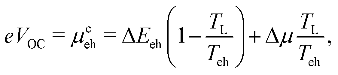
The section above introduced the basic concept of a hot-carrier solar cell and identified the relaxation time τre as the most crucial parameter to achieve a high PCE in such devices. This bears the question of how carrier cooling predominantly occurs and what choice of material and engineering strategies could improve this parameter. The following section is thus devoted to discussing the energy loss mechanisms of hot carriers. This discussion is based on materials with a relatively simple composition and crystal structure – less symmetric structures can exhibit more complex decay routes for which a detailed discussion goes beyond the scope of this review.Incident photons generate electrons and holes at elevated positions in the band structure of an absorber (consider Fig. 3(a), (1)). These carriers quickly assume an equilibrium amongst each other through elastic carrier–carrier scattering (2, 3) and at increasingly higher carrier concentrations also through impact ionisation (II) and Auger recombination (AR). Having equilibrated, electrons and holes will occupy states according to Fermi–Dirac statistics, allowing for assigning the temperatures Te and Th to the carrier distributions. The equilibration process is therefore called thermalisation. These temperatures are (much) larger than the lattice temperature of the absorber (TL) – thus the term “hot carrier” – and are generally not identical. The time needed for this process is the time τth and is of the order of 100 fs in most materials. The populations of hot carriers also generate a dynamic quasi-Fermi level μe and μh for electrons and holes (separation Δμ), respectively. For the limiting case of small carrier densities or localised carriers the effect of carrier–carrier scattering is negligible and the charges will directly undergo the process discussed in the following.
 | ||
| Fig. 3 Schematic of the charge carrier distribution in the valence (VB) and conduction band (CB) of an arbitrary semiconductor with a narrow band gap (a). When in equilibrium (0), charge carriers are thermally excited into the bands and have the same temperature as the lattice. Photoexcitation promotes an excess amount of electrons into the CB and holes into the VB (1). Ultrafast elastic carrier-carrier scattering will set in (2) and transform the non-equilibrium carrier distribution to a thermal distribution of hot carriers in the CB/VB (3). Carrier cooling (4) will equilibrate the temperatures before eventual carrier recombination. The schematic in (b) displays the cooling for electrons and holes in parabolic bands of unequal curvature (thus different carrier effective masses). In polar materials, the initial energy loss predominantly occurs through the emission of longitudinal optical phonons (ELO) and many classical materials exhibit slow cooling only for hot electrons. | ||
In a real absorber, these hot carriers will successively interact with the lattice through phonons and lose their excess energy (Fig. 3(b)). This reduces Te and Th, until both are equal to TL (4). The time needed for this process is the relaxation or cooling time τre (sometimes this is also referred to as thermalisation, but for clarity we reserve this term for the first, i.e. carrier–carrier scattering, stage) and is commonly shorter than 1 ps. Finally, carriers will recombine with each other until an equilibrium of electrons and holes due to thermal excitation is reached (0).
In polar compound semiconductors, energy loss through carrier–lattice interactions predominantly occurs through the Fröhlich interaction with longitudinal optical (LO) phonons (consider band structure in Fig. 3(b)). Interaction with acoustic phonons also takes place, but chiefly around the zone-centre, where these exhibit negligible energy. Lattice anharmonicity allows for optical phonons to further decay into acoustic phonons through several mechanisms. Given the low thermal conductivity attributed to optical phonons, the heat dissipation from the absorber (i.e. the eventual loss mechanism) occurs through acoustic phonons. As a first means to prolong carrier cooling times, a low optical phonon energy will decrease the energy lost in this initial step of the Fröhlich interaction. Lower phonon energies are generally found for materials with heavier atoms or stronger interatomic interaction (force constants, see below).
A viable path to increase the relaxation time seems to be the suppression of the further decay of LO into acoustic phonons (as depicted in Fig. 4(a)) by forming a so-called “phonon bottleneck”.36 In presence of such a bottleneck, carrier cooling will rapidly build up a population of hot phonons at some point in the decay cascade, which then can emit their energy to reheat the charge carriers.37
 | ||
| Fig. 4 Phonon dispersion relation for the case of a diatomic material in 3D with degenerate transverse modes. Phonon decay routes predominantly originate in zone-centre LO phonons, to progressively turn into acoustic phonons of smaller energy that dissipate the heat from the material (a). Schematic of major decay routes for LO phonons as discussed in the main text (b). Note that for simplicity, only relevant phonon branches are included in (b) and that contrary to these simple sketches, both energy and momentum need to be conserved. | ||
To discuss how a smart choice of materials could create such a bottleneck, we consider the illustrative case of the phonon dispersion of a diatomic material with degenerate transverse branches, as shown in Fig. 4(a). One then finds two optical branches (ELO > ETO), which are degenerate at the zone-centre and two acoustic branches (ELA > ETA), which are also degenerate at k = 0, but with vanishing energy.
For cubic materials of zincblende or diamond structure, three decay mechanisms can occur and will be discussed in the following.38 The Klemens mechanism describes the decay of one optical into two acoustic phonon – each with half of EO and equal, but antiparallel, momentum (consider Fig. 4(b)).39 Energy and momentum conservation must hold: EA,1 + EA,2 = EO and ![[k with combining right harpoon above (vector)]](https://www.rsc.org/images/entities/i_char_006b_20d1.gif) A,1 + A,2 = O. In the Fröhlich mechanism, optical phonons predominantly build up at the zone-centre, from where further decay then originates. As can be seen from Fig. 4(b), the Klemens mechanism can be suppressed for a large phononic band gap, when EA,max is smaller than 1/2EO,min. For a simple diatomic system, this is for example achieved through the choice of two atoms with large difference in mass. The maximum acoustic phonon energy at the Brillouin zone edge is
A,1 + A,2 = O. In the Fröhlich mechanism, optical phonons predominantly build up at the zone-centre, from where further decay then originates. As can be seen from Fig. 4(b), the Klemens mechanism can be suppressed for a large phononic band gap, when EA,max is smaller than 1/2EO,min. For a simple diatomic system, this is for example achieved through the choice of two atoms with large difference in mass. The maximum acoustic phonon energy at the Brillouin zone edge is
 | (2) |
 | (3) |
The next important decay process is the Ridley mechanism,40 wherein a zone-centre LO phonon decays into one TO and a low energy LA phonon: ELO → ETO + ELA (also shown in Fig. 4(b)).41 This mechanism implies a much lower energy loss to acoustic phonons than Klemens decay, which is only appreciable if there is a large LO–TO splitting around the zone-centre. For highly symmetric crystal structures, such as cubic, the LO and TO modes are almost degenerate at the zone-centre and exhibit a low dispersion – severely suppressing the efficiency of the Ridley mechanism.10 A similar route is the so-called Vallée–Bogani channel, where a LO mode decays into a lower phonon of the same branch and an acoustic mode. This mechanism was reported to be dominant in the case of GaAs.42
A decay mechanism, which is often not considered in classical HCSC literature, but recently invoked, is the energy loss through IR emission.43 In polar semiconductors, optical phonons can interact with photonic modes to form phonon–polaritons.44 With a high optical phonon occupation, as given in the presence of a phonon bottleneck, phonon–polaritons will decay through emission of IR radiation equal to ETO and a LA mode with ELA = ELO − ETO.43 A large LO–TO splitting thus again benefits the energy dissipation.
Finally, for hexagonal materials in wurtzite structure, an additional Barman–Srivastava channel opens up, where an optical phonon decays into two optical phonons of a lower branch.45 Again, a small splitting of these branches would reduce this channels efficiency. Since four-phonon processes are expected to have a negligible impact at relevant temperatures (T < 1000 K), we shall not discuss them here.46
Summarising above considerations, Conibeer and co-workers established a list of important attributes of a material that should lead to an extended carrier relaxation time τre and good performance in prospective HCSCs.10,22 According to priority, they list them as:
(i) a large phononic band gap between ELO,min and ELA,max, to suppress Klemens decay, (ii) a narrow dispersion of optical phonons ELO,max − ELO,min, to minimise Ridley decay, (iii) a small electronic band gap Egap – below 1 eV, to increase the absorption, (iv) a small optical phonon energy ELO, to reduce the loss energy per emitted LO phonon and (v) a small maximum acoustic phonon energy ELA,max to maximise the phonon band gap.
4 Materials showing slow carrier cooling
The experimental investigation of hot carrier lifetimes is often carried out through optical spectroscopy. In transient absorption (TA) experiments, the material's ground state usually shows a bleaching due to population of higher states after excitation (Fig. 5(a) and 7(a)). If a significant delay for the onset of the full ground state bleaching can be observed, this is often taken as evidence for a slow cooling of hot carriers, which successively relax down to the lowest excited state. Similarly, these relaxing carriers can also be probed through two-photon photoelectron spectroscopy (2PPES), which is a strong technique, but experimentally demanding and thus not as frequently used.47 In photoluminescence (PL) spectroscopy, a possible contribution of hot carriers (so-called hot photoluminescence) manifests as a high energy tail of the emission, which can be fitted to a Boltzmann distribution as approximation to extract the carrier temperature (Fig. 5(b) and 9). With increasing computer power, recent investigations have also increasingly been driven by modelling and simulation. We note that care has to be taken when analysing the results of purely optical techniques especially when heterogeneous or disordered systems are studied. Unusually long decay times in those cases may be readily explainable as the carrier transfer towards the minimum of ground states.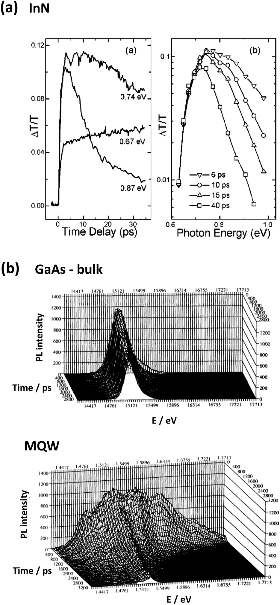 | ||
| Fig. 5 Transient absorption is one of the main methods to investigate the cooling times of hot carriers. The spectra in (a) show data for bulk InN upon excitation at 400 nm (top). The left plot shows how the absorption above the band edge (0.87 and 0.74 eV) decays with time and the ground state bleaching at 0.67 eV sets in. Reprinted from ref. 48 with the permission of AIP Publishing. The second standard technique to investigate carrier relaxation is through transient PL spectroscopy. Spectra for GaAs (b) exhibit a pronounced contribution of high emission energy from QW structures (bottom) compared to a single sharp emission peak for the bulk (top). Figure reprinted with permission from ref. 49. Copyright 1993 by the American Physical Society. | ||
4.1 Classical bulk candidates
Historically, III–V nanostructures, especially GaAs quantum wells (QWs) have been investigated intensively, because they could be manufactured at high quality and showed better performance than their bulk forms.49 However, before discussing the impact of nanostructuring, we shall take a look at bulk semiconductors that were considered or identified as suitable absorber materials.In a broad theoretical screening of materials, Conibeer et al. found a large enough phononic band gap in binary compounds including nitrides, such as InN, GaN, BiN, where the light nitrogen atom particularly favours a large phononic gap. Alternatively, also oxygen-containing compounds such as SnO or Bi2O3 were predicted with a sufficient phononic gap and both InP and AlSb were on the edge in these calculations.22,36 König et al. extended these considerations, noting that Bi based materials (AlBi or Bi2S3) seem promising and suggested to use materials with low carrier effective mass and permittivity to reduce the Fröhlich interaction.50
InN received particular attention given its relatively narrow band gap of below 0.7 eV51 and low electron effective mass of 0.055 m0.52,53 Despite early problems with growing the material at an adequate quality, a hot phonon effect could be observed for zone-centre LO modes in the wurtzite phase of InN (also for GaN). Transient absorption studies, as shown in Fig. 5(a) thus clearly exhibit a contribution of hot carriers.48 The relaxation time, however, was determined to be a fast 6.87 ps, owing to a large LO–TO splitting that allows for rapid Ridley decay.54,55 The estimated maximum PCE was thus only a modest 24%, when considering 1000 sun concentration.56 Furthermore, the scarcity of In makes compounds of more abundant materials more appealing.
Based on considerations of atomic mass and electronegativity, Conibeer et al. gave an informative overview of how the model material InN could be replaced by analogues, such as II–VI-nitride compounds, other nitrides or oxides, III–V compounds with large anion mass or group IV alloys.10 The above mentioned AlSb, for example, exhibits not only a large phononic band gap, but also a low optical phonon dispersion, which should suppress both Klemens and Ridley decay. Unfortunately, though, its band gap is about 1.5 eV and indirect – hence severely reducing its suitability for HCSCs. Ab initio investigations offered a narrower electronic band gap of 0.59 eV for BSb, which also possesses an even wider phononic gap. Although the former is still indirect, the material exhibits a strong absorption near the band edge.57 The electron effective mass is furthermore low and Ridley decay is strongly suppressed through a small LO–TO splitting of about 15 cm−1.58 GaSb, finally, was successfully implemented in a multi QW structure and will be discussed in the next section.
Group IIIA nitrides, such as YN or ScN have large elemental mass differences and could thus be thought to have a large phonon gap. When forming in rock salt structure, however, they actually do not possess a phononic gap at all.59,60 The group IVA nitrides HfN and ZrN have large predicted phonon band gaps and a small dispersion of optical modes.27,59 Both materials have zero electronic band gap, which could be an asset, if the relaxation time were long enough. Extracted values amount to approximately 3 ns in the former and 500 ps in the latter case, which is insufficient to allow for a good HCSCs performance, given the absent band gap.27,61
In summary, we can say that although there are candidate materials, which show prolonged hot carrier lifetimes and proper elemental composition can be used to engineer them, it is very challenging to maintain all other desired properties of absorber materials (electronic band gap, carrier mobility etc.). Furthermore, the observed carrier lifetimes are generally far lower than necessary for efficient HCSCs.
4.2 Nanostructures
Reduced dimensions are considered to offer several positive features for prolonged hot carrier lifetimes. A different kind of phonon bottleneck, for example, is often said to be a consequence of the discrete electron density of states (DOS) in zero-dimensional quantum dots (QDs). This DOS only allows for discrete cooling steps and might thus hamper the relaxation. With their narrow band gap and comparatively mature chemistry, lead chalcogenide colloidal quantum dots have been interesting candidates in this respect.62 Similarly, graphene quantum dots have attracted considerable research interest after a reported hot carrier lifetime in excess of 100 ps.63 A problem, however, is that the increased carrier confinement also increases Auger recombination,64 which can reduce the relaxation time. More importantly, an efficient HCSC needs to possess a strong absorption over a broad spectral range – a property QDs, with their discrete DOS, cannot deliver. Ensembles of QDs, as used in thin film solar cells, on the other hand, will offer additional decay channels through their finite size distribution.Engineering superlattice (SL) structures based on multiple QWs, might be a way to create favourable phonon bands that reduce the carrier relaxation, for example by opening up a phonon band gap at the mini-Brillouin zone boundaries.22,44,53,65 Analogous to the discussion above, Klemens decay will be suppressed if no LA phonon states are available at half the energy of zone-centre optical phonons. In contrast to QDs, QWs also possess a continuous electron DOS, leading to a broad spectral coverage and much expertise has been acquired in the manufacturing of such QW structures through epitaxial growth, e.g. of III–V compounds.
It needs to be stated, though, that despite the compelling theory of the opening of a phonon gap, the increased relaxation times presented in the following might be explained by different processes and possibly by their combined effects. Firstly, contrary to the bulk, charge carrier diffusion in QW structures might be impeded. Carrier diffusion, however, tends to reduce the concentration of hot carriers and decreases the density of hot LO phonons emitted by these carriers. Secondly, QWs posses low or negligible overlap between the well and barrier materials' optical phonon DOS. The zone-centre LO phonons emitted by hot carriers in the well might then be reflected by the barrier and increase the phonon bottleneck.10
Also noteworthy, favourable consequences of quantum confinement affecting the phononic band structure may be overcompensated by detrimental effects through surface phonons.66 The role of nanostructures on carrier cooling is thus not straightforward and needs to be investigated closely in every specific case. Additionally, we would like to note, that care has to be taken when carrier temperatures for nanostructures are solely based on PL studies, as the contribution of higher electronic states in the wells can have non-trivial effects on emission spectra.67
Early on, a slower carrier cooling in GaAs/AlGaAs QWs compared to bulk GaAs was observed and sparked great interest into these structures (consider Fig. 5(b) for a comparison of transient PL spectra).49,68 This behaviour was explained by a phonon bottleneck setting in at lower carrier density in the former case. For GaAs or InP, a phonon gap was later also observed in nanowires, which highlights the power of nanoengineering on desired material properties.69,70
Research highlights on such systems include a long carrier relaxation time of 5.8 ps in GaAsP/InGaAs quantum wells with a steady state carrier temperature of 100 K above TL under 10000 sun equivalent illumination.71 The corresponding material thermalisation coefficient Qth was 9.5 W K−1 cm−2, compared to GaSb with around 80 W K−1 cm−2.20 The same group also reported a successful extraction of hot carriers from an InGaAs QW at low temperature (although only 35 K above TL).72
As an important observation, a device consisting of five InGaAsP quantum wells was investigated by Rodière et al. and both the carrier temperature and quasi-Fermi energy splitting were determined.73 The latter was observed to exceed the energy of the absorption onset, which is a decisive characteristic for a hot carrier absorber. In a detailed study, Nguyen et al. recently reported the increase of current and voltage in an InGaAsP based quantum well heterostructure attributed to the contribution of hot carriers. Their devices achieved 11.6% PCE under monochromatic illumination with an incident power close to maximum solar concentration (equivalent to 55600 suns).74
For superlattices of InAs/GaAs quantum dots, a high carrier temperature exceeding 1000 K with a hot carrier lifetime approaching 1 ns was furthermore observed and attributed to restrictions in phase space and energy-momentum conservation. The corresponding heat dissipation rate of the QDSL was said to be one order of magnitude better than for multi quantum well structures.75
The encouraging success of QW structures and SLs is strongly linked to the community's great experience with the fabrication of these nanostructures at high quality and precision in epitaxial processes. We can thus hope that further research on the deposition of such structures based on different materials can improve these results for HCSC application. As a beneficial side effect, QW structures could also conveniently be used to simplify the device fabrication as shown in Fig. 6.20,31 Semi-selective extraction contacts could, for example, easily be integrated by using materials with different effective masses for electrons and holes and be fabricated monolithically in one manufacturing process.
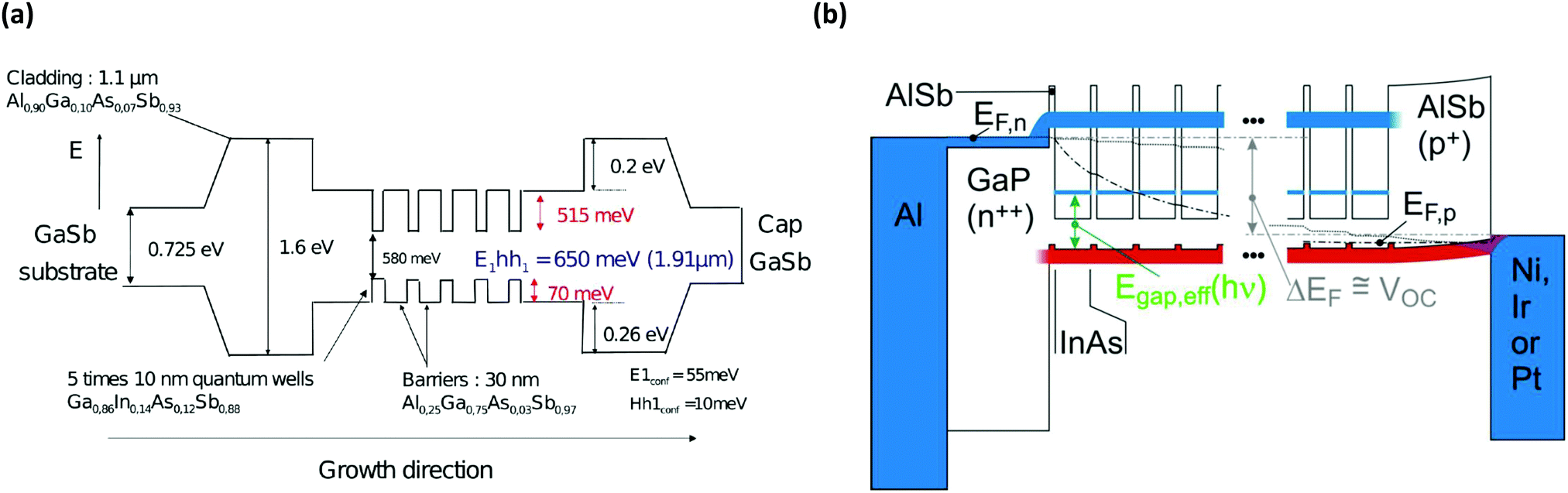 | ||
| Fig. 6 Epitaxially grown multi QW structures based on III–V semiconductors offer the possibility to exploit the benefits of nanostructuring whilst including semi-selective extraction contacts through mere compositional variation. Five 10 nm thick wells of InGaAsSb were sandwiched between 30 nm thick AlGaAsSb barriers and were cladded by AlGaAsS of wider band gap to test the thermalsiation rate in the well (a).20 The structure in (b) is based on InAs wells sandwiched between AlSb barriers and includes a thick GaP and AlSb semi-selective extraction contact integrated into the lattice matched architecture.31 Reproduced from ref. 20 with permission from The Royal Society of Chemistry. Reprinted from ref. 31 with the permission of AIP Publishing. | ||
4.3 Perovskites
Metal halide perovskites (HaPs) have become a centre of attention in the field of photovoltaic materials. Their high efficiency, solution processability and versatile composition make them an attractive research object. Importantly, also long hot carrier lifetimes have been reported in several publications. | ||
| Fig. 7 Normalised transient absorption spectra of MAPbI3 can be fitted at higher energy to extract the cooling rates and carrier temperature as a function of time (a). The spectra were taken with a delay ranging from 0.1 to 1.5 ps.76 Initial temperatures exceeding 2000 K were reported upon excitation at 400 nm (red circles, 500 nm shown in blue) (b).77 The extraction of the correct information from the TA spectra (red line in (c)) is made complex by several contributions to the signal. The yellow line in (c), for example, indicates the modified joint density of states (unperturbed in black) after band filling of the carriers (blue shaded region) and band gap renormalisation (black dashed line). The green dotted line denotes the Fermi–Dirac distribution of the charge carriers and the excitation pulse is shown in blue.78 Images (a) used in accordance with the Creative Commons Attribution license (https://creativecommons.org/licenses/by/4.0/). (b) Reproduced from ref. 77 with permission from The Royal Society of Chemistry. (c) Reprinted by permission from Springer Nature, Nature Photonics, Copyright 2015. | ||
It is important to note that although highly informative and available with high temporal resolution, TA studies offer especially complex spectra in this class of materials. Effects, such as band gap renormalisation, state filling, ground state bleaching and refractive index changing need to be considered for a proper analysis (consider sketch in Fig. 7(c)).78 For short time scales below 0.5 ps, it is also important to note that carrier thermalisation was reported to occur within 100 fs, (depending on the excitation density, values between 10 to 85 fs were found for 1018 and 1019 cm−3).80,81
Hot PL emission, which is easier to analyse, was also observed experimentally. A rise time of around 0.2–0.5 ps for band edge emission was reported upon excitation at 450 nm.82 More recently, a time scale as long as 100 ps was reported, which strongly depended on the carrier excess energy.83
Such promising lifetimes in MAPbI3 directed increased attention to different compositions. For the MAPbBr3 variant or halide mixtures of Br:I, again a rise time of the ground state bleaching could be observed in TA experiments and was linked to slow hot carrier cooling.81,84 The reduction of the cooling time for larger bromine contents was attributed to the change in crystal structure (from tetragonal to pseudocubic), which was said to entail a broadening of the conduction band (larger electronic DOS) as well as an increase in electron–phonon coupling and phonon propagation. These investigations thus suggest that amongst HaPs, iodine-based compounds are most promising for HCSCs.
The role of the A-site cation was investigated by Yang et al. using ab initio calculations and ultrafast spectroscopy. Amongst the three pure APbI3 compositions (A being MA, formamidinium (FA) or cesium), longer relaxation times were found for the two hybrid organic–inorganic materials compared to the Cs-based all-inorganic variant.85 FAPbI3, in particular, exhibited a tenfold longer relaxation time than the Cs counterpart, which is in line with further reports on CsPbI3.86 From transient PL spectra, Zhu et al. deduced a hot carrier lifetime exceeding 100 ps (150 and 190 ps)87 in single crystals of the bromine variants MAPbBr3 and FAPbBr3, but no effect for CsPbBr3. They also reported two distinct carrier cooling regimes for MAPbBr3 and FAPbBr3. Beyond 0.5 ns, the temperature decay became very slow and reached 680 K after 10 ns. Such long lifetimes for the bromine compounds seem to contradict the observations of the previous paragraph, i.e. a shorter cooling time for Br-containing compositions, but it has to be noted that these measurement were carried out on single crystals, which could show longer lifetimes due to a lower defect concentration or reduced interface effects.
In a separate study, Madjet et al. calculated the hot carrier relaxation in APbI3.88 They found a strong dependence on the A-site cation and a slower relaxation of both hot electrons and hot holes in the all-inorganic CsPbI3 explained through the reduced interaction between the Cs cations and the Pb–I frameworks. As noted above, these findings are in contradiction to many other reports.
We note, however, that care needs to be taken when making these comparisons, since different compositions can also exhibit different crystal structures with different phonon dispersions – the origin in changed cooling rates might thus not lie in molecular re-orientation, but changed phonon structure. Also, what has been mentioned already, the profound impact of the excitation intensity, has to be taken into account when comparing different systems and experiments.89
Emerging from the increasing number of publications on hot carriers in Pb-based HaPs is that at least two pronounced cooling stages seem to be present. Depending on the employed analysis technique and sample, the first one lies on a sub-picosecond to 2 ps scale. This primary temperature decrease occurs from values as large as 2800 K for FAPbI3, for example.85 The second stage can extend to several hundreds of picoseconds up to the nanosecond regime. Given that these stages could be affected differently by compositional changes, this aspect could also mediate contradictory statements in the literature.
So far, explanations for the long hot carrier lifetimes in perovskites have been diverse and in the light of distinct cooling stages, it seems likely that more than one effect is relevant. Following the above discussion, the dissipation of the excess energy will first occur through phonon emission of hot carriers (Fröhlich interaction), followed by optical phonon decay and finally by the conduction of heat out of the system through acoustic phonons.
Starting from short-term to long-term effects, Kawai et al. carried out ab initio calculations showing that 0.6 eV below the VB maximum in CsPbI3, the cooling of holes is impeded due to a small electronic DOS. The corresponding cooling time was determined to 0.5 ps and it was suggested that this effect was independent of the A-site cation.91 This theory was, however, contested through reports that find differences in the decay upon A-cation variation.47 A recurring observation is a prolonged initial relaxation time for higher carrier densities. This is commonly attributed to a phonon bottleneck.76,84,92 Values for this cooling time, however, range from 230 to 300 fs to a few picoseconds in these report.
There is a general agreement that charge carriers in HaPs strongly couple to LO phonons through the Fröhlich mechanism. Although varying slightly, the relevant phonon energies were determined to lie between 10 and 20 meV.81,93,94 The IR spectrum of hybrid HaPs consists of three different regions, in case of MAPbI3, for example, the internal vibrations of the MA cation between 100–380 meV, its librations between 17 and 22 meV and the vibration of the inorganic sublattice at frequencies below 17 meV,95,96 Consequently, the interaction of carriers predominantly occurs through the metal–halide cage (specifically the Pb–I stretching and Pb–I–Pb rocking modes) that also dominates the static permittivity. Bromine-perovskites were shown to exhibit a stronger coupling as a result of their smaller high-frequency permittivity and an increased phonon energy is generally found when going from the heavy I− to the lighter Cl− anions.97
Such low LO phonon energies have two important consequences beneficial for HCSCs. Firstly, a high number of phonons has to be emitted for a carrier to cool to the band edge. Secondly, these modes are already highly populated at RT and further LO emission could bring the system quickly to a situation where phonon re-absorption becomes relevant. The superior performance of iodine compounds might thus (in part) be explained by their lower LO phonon energy.
For the second stage, i.e. optical-acoustic phonon decay, a proposition close to the discussion above for the classical materials is the suppression of Klemens decay through a large phonon band gap. Additional to a long lifetime of 0.6 ps for zone-centre LO phonons at moderate densities (1018 cm−3), Fu et al. calculate ħωLO = 8 meV and ħωLA = 2.5 meV, which suggest the existence of such a phonon band gap in MAPbI3.90 Similarly, Yang et al. observed a drastic increase in carrier cooling time from 30 fs to 30 ps upon high excitation intensity in thin films of MAPbI3 and FAPbI3 and propose this to be a consequence of a phononic band gap due to mass differences of the ions or due to ferroelectricity.78 Notably, though, the calculated LO energy of 8 meV is much lower than the value determined above, casting doubts on the relevance of this calculation. Ridley decay, on the other hand, should be an efficient loss mechanism, since a strong splitting of LO–TO modes was reported.97 Importantly, the complexity of the crystal structure and possible hybrid acousto-optical phonon modes generally suggest that simple considerations as made above for the binary compounds are invalid or incomplete for HaPs.
On the other hand, a weak interaction between LO phonons and acoustic modes was indeed reported by Monahan et al. through 2D spectroscopy on a MAPbI3 sample. They observed long-lived coherent LO phonon oscillations around 0.9 THz (3.7 meV, which is smaller than above mentioned phonon energies), which they assign to angular distortions of the inorganic cage.98 This suggests a strong coupling of the LO phonon mode to the electronic excitation, but a weak interaction with the remaining phonon modes (else the decoherence would be much faster). Explicitly, the angular distortions do not couple to the molecular rotations.
All of these reports show that significantly more work into a proper understanding of the dispersion and the interaction of the different components will be needed to adequately discuss the decay routes. Phonon dispersion relations are thus a key investigation for the optimisation of HaPs for hot carrier applications.99
Interesting observations in this respect stem from the comparison of the hybrid compounds with all-inorganic Cs-based HaPs. A more pronounced phonon bottleneck in hybrid organic–inorganic materials was found compared to the Cs-based all-inorganic variant, suggesting an important role of the organic cation.85 For MAPbBr3 or MAPbI3, for example, optical phonons were observed through inelastic neutron scattering to be strongly anharmonic and a clear order–disorder transition associated with the MA tumbling mode was observed for the different crystal structures (tetragonal and orthorhombic) around 150 K.100,101 Fittingly, hot PL was observed only at elevated T in the cubic or tetragonal phase, but completely vanished for the orthorhombic phase at 77 K.87
As an additional mechanism at the late stage of relaxation, especially at high carrier densities exceeding 1019 cm−3, Auger heating was also proposed to dominate the carrier temperature.90 In this process, recombining carriers transfer their energy to heat other carriers in the material and thereby increase the temperature (consider Fig. 8(a and b)).
 | ||
| Fig. 8 Several studies on perovskites report two distinct cooling stages as seen in (a).90 Here, the experimentally determined temperature decay (red circles) is explained by an initial hot phonon effect (HP) and Auger heating (AH) at later stages. The band scheme in (b) depicts how the Auger process involves the non-radiative recombination of a an electron hole pair (red arrow) and the energy is transferred to a low energy electron, thus increasing the temperature in the conduction band. Alternative theories include the acousto-optical up-conversion of phonons that re-excite the carriers. Such a pathway is depicted in (c) for the phonon structure of FAPbI3. Where initial LO emission (1) and phonon decay (2) are followed by up-conversion (4) and carrier heating (5).85 Images used in accordance with the Creative Commons Attribution license (https://creativecommons.org/licenses/by/4.0/). | ||
Finally, if optical phonons successfully decay into acoustic phonons, the third stage of energy dissipation expects them to transport the energy irreversibly out of the system. If, however, these acoustic phonons cannot leave the material, their energy may be used to re-excite optical phonons. Their propagation could, for example, be blocked due to strong anharmonic phonon–phonon scattering. For MAPbI3, acoustic phonons were reported to have a nanoscale mean free path (below 10 nm) and considered to be responsible for the small thermal conductivity (in single crystals measured to the extremely low value of 0.5 W m−1 K−1).102 Yang et al. concomitantly propose such a case, and argue that the up-conversion of acoustic phonons could increase the phonon bottleneck (Fig. 8(c)).85 Phonon up-conversion was furthermore suggested to be stronger in hybrids, because of overlapping phonon branches and FAPbI3 was identified as the best candidate. In contrast to the Klemens hypothesis invoked above, Yang et al. also suggest that there was no acousto-optical phonon band gap.
This acousto-optical up-conversion hypothesis was, however, also challenged based on the long dephasing time of the 0.9 THz mode (several ps). This was interpreted as weak interaction between LO and acoustic modes,98 but it is important to note, that the up-conversion mechanism was assumed to become relevant at longer delays (exceeding 10 ps) than relevant for the dephasing.
An additional mechanism not discussed so far, but with considerable impact and especially debated in the field of HaPs at the moment, is the formation of large polarons.103–105 Niesner et al. observed energetic electrons 0.25 eV above the CB minimum with a lifetime as long as 100 ps in MAPbI3.47 Contrary to what leads to the phonon bottleneck assumption, they observe an increase in cooling rate upon increasing the carrier density in the low carrier regime of 1016–1017 cm−3. Their proposition is that a large polaron, formed by the re-orientation of the organic cation around the charge carrier, works as a protective shield against LO phonon scattering. Increasing polaron concentration upon higher excitation densities is then assumed to destabilise the polarons due to Coulomb repulsion and thereby reduce the lifetime-enhancing effect. This assumption was backed up by Frost et al., who identified the Mott density (when polarons start to overlap) in MAPbI3 to be around 1018 cm−3.106
Zhang et al. supported the proposition of the reorientational motion of MA molecules to lead to the pronounced hot fluorescence in MAPbBr3.107 In a recently published time domain ab initio study they showed that depending on the MA orientation, low energy structures give rise to polaron-like electrons and holes, whilst the higher energy structures lead to more delocalised wavefunctions – interpreted as free carriers. They hence propose a two-emitter system of the MAPbBr3 perovskite with hot and regular luminescence components. The energy difference between them is about 0.3 eV and the hot fluorescence lifetime is of the order of several hundreds of picoseconds. On the other hand, Bretschneider et al. suggest that polaron formation was governed by the inorganic cage and the formation was thus independent of the A-site cation.108
An additional side-effect of the presence of large polarons would furthermore be that these lead to a strong scattering of acoustic phonons, i.e. a randomisation of the phonon momentum, which entails a low thermal conductivity.103 In other words, large polaron formation could have two beneficial effects: the suppression of the initial interaction with LO phonons and the suppression of heat dissipation from the absorber material via acoustic phonons. Nonetheless, some reports also consider hot carrier cooling and polaron formation as competing mechanisms,87 with the latter setting in after 250–300 fs (based on the cation orientation) for MAPbI3.47,109
From a technological point of view, an important aspect is furthermore the distance hot carriers might be able to travel. Also in this respect, very promising data were reported. In MAPbI3, a quasi-ballistic transport regime that is followed by transport at non-equilibrium temperature were observed with corresponding carrier travel distances of 230 and 600 nm.110 Such values would allow a significant portion of the hot carriers to reach the extraction contacts in films of around 500 nm thickness, as commonly used to maximise absorption.
Whilst several different theories for the long hot carrier lifetime have thus been proposed, a deeper insight into the material properties, especially the phonon dispersion and phonon interaction will be needed for an adequate understanding. Recently, also structural fluctuations and the interaction of the organic cation with the inorganic cage in hybrid HaPs have increasingly moved into the centre of attention and seem to be responsible for many of the materials' interesting properties.111
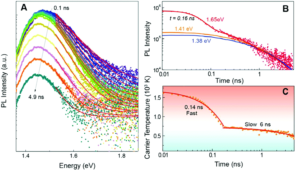 | ||
| Fig. 9 PL spectra of a FASnI3 thin film taken at different times after excitation A. The high energy side of the spectrum was fitted with a Boltzmann distribution (red lines), from which the temperature in C was extracted. The PL transients at high and low energy are given in B and show the pronounced contribution of hot photoluminescence around 1.65 eV at early delays. The temperature decay in C exhibits to distinct decay regions with a lifetime of 0.14 and 6 ns respectively.112 The carrier temperature, again clearly follows two different decay mechanisms with a time constant of 0.14 and 6 ns (bottom right). Image used in accordance with the Creative Commons Attribution license (https://creativecommons.org/licenses/by/4.0/). | ||
As with the origin of the long lifetime in lead-based perovskites, the reason for the much better performance in this tin compound is not clear at this moment. It is noteworthy, though, that an ultra low thermal conductivity of around 0.09 W m−1 K−1 was reported for the MA variant, which is even lower than the one found in MAPbI3 (0.5 W m−1 K−1).117 This suggests that the poor escape of heat plays an important role in the favourable characteristics, possibly through the acoustic phonon up-conversion mechanism.
Papagiorgis et al., for example, investigated FAPbI3 nanocrystals both in solid and colloidal state using TA spectroscopy. They find a delayed onset of the ground state bleaching and a broadening of its high energy tail.118 Extracting the dynamics of the delayed onset, they discussed three distinct carrier cooling stages: firstly the interaction with LO phonons on a sub-picosecond timescale, which can be slowed down with higher carrier densities (phonon bottleneck), secondly, a build-up of a hot phonon population either due to a high phonon emission rate78 or acousto-optical phonon up-conversion and thirdly, after 40 ps, Auger heating.85 The authors furthermore note that hot carriers can also be trapped in states above the band gap in presence of unreacted precursors in non-purified samples. At least for the bulk, however, carrier cooling was previously reported to be a trap free process.83
Chung et al. investigated the hot carrier relaxation dynamics in CsPbI3, CsPbBr1.5I1.5 and CsPbBr3 nanocrystals through TA spectroscopy and through electronic band structure calculations.119 All samples exhibited a fast hot carrier relaxation below 0.6 ps, with the pure Br variant giving the shortest and the pure I-based compound the longest lifetime. This observation was linked to electronic DOS of holes in the VB – similar to the case of CsPbI3 reported for the bulk above. For CsPbI3 Shen et al. observed a cooling time of around 10 ps upon increasing the carrier density beyond 7 × 10⁻¹⁸ cm−3.120
Li et al., finally, considered MAPbBr3 nanocrystals of different size and a microcrystalline thin film.66 They observed a long hot carrier lifetime attributed to a phonon bottleneck and Auger heating (depending on the carrier density). Carrier thermalisation occurred within 150 fs after excitation and they reported an initial carrier temperature of 1700 K for NCs, which is four times larger than the one for the bulk sample. Using an excess excitation energy of 0.7 eV and similar carrier densities of 1018 cm−3, the cooling time of bulk MAPbBr3 was given as being lower than 0.8 ps. For large NCs, it can be as long as 32 ps at comparable carrier densities. At low pump fluence, carriers were observed to cool faster with increasing NC size. The initial relaxation was attributed to LO phonons (independent of NC size or NC vs. bulk) until the carrier temperature was around 700 K. In the second and slower cooling stage, the decay was said to be governed by the equilibrium between LO and acoustic phonons. The estimated hot carrier diffusion length was, unfortunately, lower than in the reports above and only amounted to 16–90 nm.
As first encouraging measurements, Guo et al. investigated coherent longitudinal acoustic phonons and reported that acoustic phonons in 2D perovskites show a significantly lower group velocity and propagation length in cross-plane direction when compared to the 3D counterparts.121 This was attributed to a large acoustic impedance mismatch between the alternating layers of perovskites and bulky organic cations. Consequently, Jia et al. carried out a femtosecond TA study on (BA)2(MA)n−1PbnI3n+1 2D perovskite and reported an increased hot carrier lifetime for n = 2 or 3, leading to a relaxation time of 1000 ps in the latter case, i.e. tenfold longer than the 3D variant.122 Again, this was attributed to a limited acoustic phonon propagation leading to phonon up-conversion.
These investigations thus clearly show the large potential of perovskite materials for property tailoring through compositional variation.
5 Conclusions
In this paper, we reviewed the advances of the community's understanding of the working mechanism of hot carrier solar cells and what we can reasonably expect as realistic power conversion efficiency based on materials that might be within reach of manufacturing. The central finding is that a hot carrier lifetime of around 1 ns is necessary to promote acceptable efficiencies. The role of the energy selective extracting contacts was also briefly discussed and here a width of around kBT seems to suffice in order to allow for a PCE of around 50%. We discussed the carrier cooling mechanisms and phonon decay routes based predominantly on simple diatomic materials and showed how such considerations led to encouraging results for classical bulk materials (such as compounds of heavy atoms with nitrogen) or nanostructures (quantum well superlattices, for example).These insights were used to put recently reported results on the interesting class of metal halide perovskites into perspective. Whilst the origin of the long hot carrier lifetimes for this material class is not yet resolved, some trends could be observed through compositional variation and it seems that iodine- and formamidinium-based compounds show the best performance. The recent report of an even greater effect in tin-based perovskites suggests that there is still a large room for improvement and that metal halide perovskites have the potential to really enable the fabrication of efficient hot carrier solar cells.
It is our strong opinion that the perovskite research community now has to take the second step and go beyond a mere reporting of long cooling times in different systems. The assignment of mechanisms for this intriguing behaviour so far seems to be often based on small evidence and we suggest that a proper understanding of the phonon dispersion relations and the phonon decay pathways will offer the necessary deeper insights. What strikes us as an important property of this material class, is the extremely low thermal conductivity found for Pb-based perovskites and supposedly even more so for the Sn-counterparts. We thus argue that the thermal properties, namely a severely restricted heat loss to the environment likely plays a major role.
Conflicts of interest
There are no conflicts to declare.Acknowledgements
This work was financed through the Materials for Sustainability (Mat4Sus) programme (grant number 739.017.005) of the Netherlands Organisation for Scientific Research (NWO).Notes and references
- M. A. Green, Y. Hishikawa, E. D. Dunlop, D. H. Levi, J. Hohl-Ebinger and A. W. Ho-Baillie, Prog. Photovoltaics Res. Appl., 2018, 26, 3–12 CrossRef.
- W. Shockley and H. J. Queisser, J. Appl. Phys., 1961, 32, 510–519 CrossRef CAS.
- L. C. Hirst and N. J. Ekins-Daukes, Prog. Photovoltaics Res. Appl., 2011, 19, 286–293 CrossRef.
- W. Peter, Physics of Solar Cells From Principles to New Concepts, Wiley, 2005 Search PubMed.
- M. A. Green and S. P. Bremner, Nat. Mater., 2017, 16, 23–34 CrossRef PubMed.
- O. E. Semonin, J. M. Luther, S. Choi, H.-Y. Chen, J. Gao, A. J. Nozik and M. C. Beard, Science, 2011, 334, 1530–1533 CrossRef CAS PubMed.
- B. Ehrler, M. W. B. Wilson, A. Rao, R. H. Friend and N. C. Greenham, Nano Lett., 2012, 12, 1053–1057 CrossRef CAS PubMed.
- R. T. Ross and A. J. Nozik, J. Appl. Phys., 1982, 53, 3813–3818 CrossRef CAS.
- L. C. Hirst, M. P. Lumb, R. Hoheisel, C. G. Bailey, S. P. Philipps, A. W. Bett and R. J. Walters, Sol. Energy Mater. Sol. Cells, 2014, 120, 610–615 CrossRef CAS.
- G. Conibeer, S. Shrestha, S. Huang, R. Patterson, H. Xia, Y. Feng, P. Zhang, N. Gupta, M. Tayebjee, S. Smyth, Y. Liao, S. Lin, P. Wang, X. Dai and S. Chung, Sol. Energy Mater. Sol. Cells, 2015, 135, 124–129 CrossRef CAS.
- P. Würfel, Sol. Energy Mater. Sol. Cells, 1997, 46, 43–52 CrossRef.
- D. J. Farrell, Y. Takeda, K. Nishikawa, T. Nagashima, T. Motohiro and N. J. Ekins-Daukes, Appl. Phys. Lett., 2011, 99, 97–100 Search PubMed.
- A. Luque and A. Martí, Phys. Rev. Lett., 1997, 78, 5014–5017 CrossRef CAS.
- C. Clavero, Nat. Photonics, 2014, 8, 95–103 CrossRef CAS.
- S. C. Limpert and S. P. Bremner, Appl. Phys. Lett., 2015, 107, 073902 CrossRef.
- M. Green, Third Generation Photovoltaics: Ultrahigh Efficiency at Low Cost, Springer, Berlin, 2003 Search PubMed.
- D. König, D. Hiller, M. Zacharias, S. Michard and C. Flynn, Prog. Photovoltaics Res. Appl., 2014, 22, 1070–1079 CrossRef.
- Y. Takeda, T. Ito, T. Motohiro, D. König, S. Shrestha and G. Conibeer, J. Appl. Phys., 2009, 105, 074905 CrossRef.
- A. Le Bris and J. F. Guillemoles, Appl. Phys. Lett., 2010, 97, 2008–2011 CrossRef.
- A. Le Bris, L. Lombez, S. Laribi, G. Boissier, P. Christol and J.-F. Guillemoles, Energy Environ. Sci., 2012, 5, 6225 RSC.
- Y. Takeda, T. Motohiro, D. König, P. Aliberti, Y. Feng, S. Shrestha and G. Conibeer, Appl. Phys. Express, 2010, 3, 104301 CrossRef.
- G. Conibeer, N. Ekins-Daukes, J.-F. Guillemoles, D. König, E.-C. Cho, C.-W. Jiang, S. Shrestha and M. Green, Sol. Energy Mater. Sol. Cells, 2009, 93, 713–719 CrossRef CAS.
- Y. Takeda, A. Ichiki, Y. Kusano, N. Sugimoto and T. Motohiro, J. Appl. Phys., 2015, 118, 124510 CrossRef.
- S. Su, T. Liao, X. Chen, G. Su and J. Chen, IEEE J. Quantum Electron., 2015, 51, 4800208 Search PubMed.
- S. K. Shrestha, P. Aliberti and G. J. Conibeer, Sol. Energy Mater. Sol. Cells, 2010, 94, 1546–1550 CrossRef CAS.
- Y. Liao, P. Zhang, S. Bremner, S. Shrestha, S. Huang and G. Conibeer, Adv. Funct. Mater., 2017, 27, 1605348 CrossRef.
- S. Shrestha, S. Chung, Y. Liao, P. Wang, W. Cao, X. Wen, N. Gupta and G. Conibeer, Jpn. J. Appl. Phys., 2017, 56, 08MA03 CrossRef.
- J. G. Labram, N. D. Treat, Y.-H. Lin, C. H. Burgess, M. A. McLachlan and T. D. Anthopoulos, Adv. Funct. Mater., 2016, 26, 1656–1663 CrossRef CAS.
- D. M. Balazs, K. I. Bijlsma, H.-H. Fang, D. N. Dirin, M. Döbeli, M. V. Kovalenko and M. A. Loi, Sci. Adv., 2017, 3, eaao1558 CrossRef PubMed.
- S. Kahmann, M. Sytnyk, N. Schrenker, G. J. Matt, E. Spiecker, W. Heiss, C. J. Brabec and M. A. Loi, Adv. Electron. Mater., 2018, 4, 1700348 CrossRef.
- D. König, Y. Takeda and B. Puthen-Veettil, Appl. Phys. Lett., 2012, 101, 153901 CrossRef.
- S. Yagi and Y. Okada, 2010 35th IEEE Photovoltaic Specialists Conference, 2010, pp. 001213 Search PubMed.
- Y. Feng, P. Aliberti, B. P. Veettil, R. Patterson, S. Shrestha, M. A. Green and G. Conibeer, Appl. Phys. Lett., 2012, 100, 053502 CrossRef.
- Y. Takeda, A. Ichiki, Y. Kusano, N. Sugimoto and T. Motohiro, J. Appl. Phys., 2015, 118, 124510 CrossRef.
- A. Julian, Z. Jehl, N. Miyashita, Y. Okada and J.-F. Guillemoles, Superlattices Microstruct., 2016, 100, 749–756 CrossRef CAS.
- G. Conibeer, D. König, M. Green and J. Guillemoles, Thin Solid Films, 2008, 516, 6948–6953 CrossRef CAS.
- H. Zhou, L. Yang and W. You, Semicond. Polym. Compos. Princ. Morphol. Prop. Appl., 2012 Search PubMed.
- G. P. Srivastava, J. Phys.: Condens. Matter, 2009, 21, 174205 CrossRef CAS.
- P. G. Klemens, Phys. Rev., 1966, 148, 845–848 CrossRef CAS.
- Y. Yao and D. König, Sol. Energy Mater. Sol. Cells, 2015, 140, 422–427 CrossRef CAS.
- B. K. Ridley, Phys. Rev. B: Condens. Matter Mater. Phys., 1989, 39, 5282–5286 CrossRef.
- F. Vallée and F. Bogani, Phys. Rev. B: Condens. Matter Mater. Phys., 1991, 43, 12049–12052 CrossRef.
- D. König, Y. Yao and R. Patterson, Jpn. J. Appl. Phys., 2014, 53, 05FV04 CrossRef.
- P. Y. Yu and M. Cardona, Fundamentals of Semiconductors, Springer Berlin Heidelberg, Berlin, Heidelberg, 1999 Search PubMed.
- S. Barman and G. P. Srivastava, Phys. Rev. B: Condens. Matter Mater. Phys., 2004, 69, 235208 CrossRef.
- D. J. Ecsedy and P. G. Klemens, Phys. Rev. B: Condens. Matter Mater. Phys., 1977, 15, 5957–5962 CrossRef CAS.
- D. Niesner, H. Zhu, K. Miyata, P. P. Joshi, T. J. S. Evans, B. J. Kudisch, M. T. Trinh, M. Marks and X.-Y. Zhu, J. Am. Chem. Soc., 2016, 138, 15717–15726 CrossRef CAS PubMed.
- F. Chen, A. N. Cartwright, H. Lu and W. J. Schaff, Appl. Phys. Lett., 2003, 83, 4984–4986 CrossRef CAS.
- Y. Rosenwaks, M. C. Hanna, D. H. Levi, D. M. Szmyd, R. K. Ahrenkiel and A. J. Nozik, Phys. Rev. B: Condens. Matter Mater. Phys., 1993, 48, 14675–14678 CrossRef CAS.
- D. König, K. Casalenuovo, Y. Takeda, G. Conibeer, J. Guillemoles, R. Patterson, L. Huang and M. Green, Phys. E, 2010, 42, 2862–2866 CrossRef.
- N. Roberto and A. Reyes-serrato, Rev. Mex. Fis., 2008, 54, 111–118 Search PubMed.
- G. J. Conibeer, D. König, M. A. Green and J. F. Guillemoles, Thin Solid Films, 2008, 516, 6948–6953 CrossRef CAS.
- G. Conibeer, R. Patterson, L. Huang, J. F. Guillemoles, D. König, S. Shrestha and M. A. Green, Sol. Energy Mater. Sol. Cells, 2010, 94, 1516–1521 CrossRef CAS.
- B. K. Ridley, J. Phys.: Condens. Matter, 1996, 8, L511–L513 CrossRef CAS.
- K. T. Tsen and D. K. Ferry, J. Phys.: Condens. Matter, 2009, 21, 174202 CrossRef CAS PubMed.
- P. Aliberti, Y. Feng, S. K. Shrestha, M. A. Green, G. Conibeer, L. W. Tu, P. H. Tseng and R. Clady, Appl. Phys. Lett., 2011, 99, 223507 CrossRef.
- S. Dalui, S. Das, S. Hussain, D. Paramanik, S. Verma and A. Pal, J. Cryst. Growth, 2007, 305, 149–155 CrossRef CAS.
- Y. Yao, D. König and M. Green, Sol. Energy Mater. Sol. Cells, 2013, 111, 123–126 CrossRef CAS.
- B. Saha, J. Acharya, T. D. Sands and U. V. Waghmare, J. Appl. Phys., 2010, 107, 033715 CrossRef.
- B. Saha, T. D. Sands and U. V. Waghmare, J. Appl. Phys., 2011, 109, 073720 CrossRef.
- S. Chung, X. Wen, S. Huang, N. Gupta, G. Conibeer, S. Shrestha, T. Harada and T. W. Kee, Sol. Energy Mater. Sol. Cells, 2017, 169, 13–18 CrossRef CAS.
- W. A. Tisdale, K. J. Williams, B. A. Timp, D. J. Norris, E. S. Aydil and X.-Y. Zhu, Science, 2010, 328, 1543–1547 CrossRef CAS PubMed.
- M. L. Mueller, X. Yan, B. Dragnea and L.-S. Li, Nano Lett., 2011, 11, 56–60 CrossRef CAS PubMed.
- V. I. Klimov, D. W. McBranch, C. A. Leatherdale and M. G. Bawendi, Phys. Rev. B: Condens. Matter Mater. Phys., 1999, 60, 13740–13749 CrossRef CAS.
- C. Colvard, T. A. Gant, M. V. Klein, R. Merlin, R. Fischer, H. Morkoc and A. C. Gossard, Phys. Rev. B: Condens. Matter Mater. Phys., 1985, 31, 2080–2091 CrossRef CAS.
- M. Li, S. Bhaumik, T. W. Goh, M. S. Kumar, N. Yantara, M. Grätzel, S. Mhaisalkar, N. Mathews and T. C. Sum, Nat. Commun., 2017, 8, 3–12 CrossRef PubMed.
- H. Esmaielpour, V. R. Whiteside, L. C. Hirst, J. G. Tischler, C. T. Ellis, M. P. Lumb, D. V. Forbes, R. J. Walters and I. R. Sellers, Prog. Photovoltaics Res. Appl., 2017, 25, 782–790 CrossRef CAS.
- J. F. Ryan, R. A. Taylor, A. J. Turberfield, A. Maciel, J. M. Worlock, A. C. Gossard and W. Wiegmann, Phys. Rev. Lett., 1984, 53, 1841–1844 CrossRef CAS.
- F. Kargar, B. Debnath, J.-P. Kakko, A. Säynätjoki, H. Lipsanen, D. L. Nika, R. K. Lake and A. A. Balandin, Nat. Commun., 2016, 7, 13400 CrossRef CAS PubMed.
- D. Tedeschi, M. De Luca, H. A. Fonseka, Q. Gao, F. Mura, H. H. Tan, S. Rubini, F. Martelli, C. Jagadish, M. Capizzi and A. Polimeni, Nano Lett., 2016, 16, 3085–3093 CrossRef CAS PubMed.
- L. C. Hirst, H. Fujii, Y. Wang, M. Sugiyama and N. J. Ekins-Daukes, IEEE J. Photovoltaics, 2014, 4, 244–252 Search PubMed.
- L. C. Hirst, R. J. Walters, M. F. Führer and N. J. Ekins-Daukes, Appl. Phys. Lett., 2014, 104, 231115 CrossRef.
- J. Rodière, L. Lombez, A. Le Corre, O. Durand and J.-F. Guillemoles, Appl. Phys. Lett., 2015, 106, 183901 CrossRef.
- D. T. Nguyen, L. Lombez, F. Gibelli, S. Boyer-Richard, A. Le Corre, O. Durand and J. F. Guillemoles, Nat. Energy, 2018, 3, 236–242 CrossRef CAS.
- Y. Harada, N. Kasamatsu, D. Watanabe and T. Kita, Phys. Rev. B, 2016, 93, 115303 CrossRef.
- M. B. Price, J. Butkus, T. C. Jellicoe, A. Sadhanala, A. Briane, J. E. Halpert, K. Broch, J. M. Hodgkiss, R. H. Friend and F. Deschler, Nat. Commun., 2015, 6, 8420 CrossRef CAS PubMed.
- O. Flender, J. R. Klein, T. Lenzer and K. Oum, Phys. Chem. Chem. Phys., 2015, 17, 19238–19246 RSC.
- Y. Yang, D. P. Ostrowski, R. M. France, K. Zhu, J. van de Lagemaat, J. M. Luther and M. C. Beard, Nat. Photonics, 2016, 10, 53–59 CrossRef CAS.
- G. Xing, N. Mathews, S. Sun, S. S. Lim, Y. M. Lam, M. Gratzel, S. Mhaisalkar and T. C. Sum, Science, 2013, 342, 344–347 CrossRef CAS PubMed.
- J. M. Richter, F. Branchi, F. V. d. A. Camargo, B. Zhao, R. H. Friend, G. Cerullo and F. Deschler, arXiv, 2017, 1701.03919.
- T. Ghosh, S. Aharon, L. Etgar and S. Ruhman, J. Am. Chem. Soc., 2017, 139, 18262–18270 CrossRef CAS PubMed.
- H.-Y. Hsu, C.-Y. Wang, A. Fathi, J.-W. Shiu, C.-C. Chung, P.-S. Shen, T.-F. Guo, P. Chen, Y.-P. Lee and E. W.-G. Diau, Angew. Chem., 2014, 126, 9493–9496 CrossRef.
- S. A. Bretschneider, F. Laquai and M. Bonn, J. Phys. Chem. C, 2017, 121, 11201–11206 CrossRef CAS.
- X. Deng, X. Wen, S. Huang, R. Sheng, T. Harada, T. W. Kee, M. Green and A. Ho-Baillie, J. Phys. Chem. C, 2016, 120, 2542–2547 CrossRef CAS.
- J. Yang, X. Wen, H. Xia, R. Sheng, Q. Ma, J. Kim, P. Tapping, T. Harada, T. W. Kee, F. Huang, Y.-B. Cheng, M. Green, A. Ho-Baillie, S. Huang, S. Shrestha, R. Patterson and G. Conibeer, Nat. Commun., 2017, 8, 14120 CrossRef CAS PubMed.
- X. Sheng, G. Chen, C. Wang, W. Wang, J. Hui, Q. Zhang, K. Yu, W. Wei, M. Yi, M. Zhang, Y. Deng, P. Wang, X. Xu, Z. Dai, J. Bao and X. Wang, Adv. Funct. Mater., 2018, 3, 1–9 Search PubMed.
- H. Zhu, K. Miyata, Y. Fu, J. Wang, P. P. Joshi, D. Niesner, K. W. Williams, S. Jin and X. Y. Zhu, Science, 2016, 353, 1409–1413 CrossRef CAS PubMed.
- M. E. Madjet, G. R. Berdiyorov, F. El-Mellouhi, F. H. Alharbi, A. V. Akimov and S. Kais, J. Phys. Chem. Lett., 2017, 4439–4445 CrossRef CAS PubMed.
- T. R. Hopper, A. Gorodetsky, J. M. Frost, C. Müller, R. Lovrincic and A. A. Bakulin, ACS Energy Lett., 2018, 2199–2205 CrossRef CAS PubMed.
- J. Fu, Q. Xu, G. Han, B. Wu, C. H. A. Huan, M. L. Leek and T. C. Sum, Nat. Commun., 2017, 8, 1300 CrossRef PubMed.
- H. Kawai, G. Giorgi, A. Marini and K. Yamashita, Nano Lett., 2015, 15, 3103–3108 CrossRef CAS.
- S. Nah, B. M. Spokoyny, C. M. M. Soe, C. C. Stoumpos, M. G. Kanatzidis and E. Harel, Nano Lett., 2018, 18, 1044 CrossRef CAS PubMed.
- A. D. Wright, C. Verdi, R. L. Milot, G. E. Eperon, M. A. Pérez-Osorio, H. J. Snaith, F. Giustino, M. B. Johnston and L. M. Herz, Nat. Commun., 2016, 7, 11755 CrossRef PubMed.
- H.-h. Fang, F. Wang, S. Adjokatse, N. Zhao, J. Even and M. Antonietta Loi, Light: Sci. Appl., 2016, 5, e16056 CrossRef CAS PubMed.
- M. A. Pérez-Osorio, R. L. Milot, M. R. Filip, J. B. Patel, L. M. Herz, M. B. Johnston and F. Giustino, J. Phys. Chem. C, 2015, 119, 25703–25718 CrossRef.
- P. Guo, J. Gong, S. Sadasivam, Y. Xia, T.-B. Song, B. T. Diroll, C. C. Stoumpos, J. B. Ketterson, M. G. Kanatzidis, M. K. Y. Chan, P. Darancet, T. Xu and R. D. Schaller, Nat. Commun., 2018, 9, 2792 CrossRef PubMed.
- M. Sendner, P. K. Nayak, D. A. Egger, S. Beck, C. Müller, B. Epding, W. Kowalsky, L. Kronik, H. J. Snaith, A. Pucci and R. Lovrinčić, Mater. Horiz., 2016, 3, 613–620 RSC.
- D. M. Monahan, L. Guo, J. Lin, L. Dou, P. Yang and G. R. Fleming, J. Phys. Chem. Lett., 2017, 8, 3211–3215 CrossRef CAS PubMed.
- A. Gold-Parker, P. M. Gehring, J. M. Skelton, I. C. Smith, D. Parshall, J. M. Frost, H. I. Karunadasa, A. Walsh and M. F. Toney, Proc. Natl. Acad. Sci. U. S. A., 2018, 115, 11905 CrossRef CAS PubMed.
- A. Létoublon, S. Paofai, B. Rufflé, P. Bourges, B. Hehlen, T. Michel, C. Ecolivet, O. Durand, S. Cordier, C. Katan and J. Even, J. Phys. Chem. Lett., 2016, 7, 3776–3784 CrossRef PubMed.
- B. Li, Y. Kawakita, Y. Liu, M. Wang, M. Matsuura, K. Shibata, S. Ohira-Kawamura, T. Yamada, S. Lin, K. Nakajima and S. F. Liu, Nat. Commun., 2017, 8, 16086 CrossRef CAS PubMed.
- A. Pisoni, J. Jaćimović, O. S. Barišić, M. Spina, R. Gaál, L. Forró and E. Horváth, J. Phys. Chem. Lett., 2014, 5, 2488–2492 CrossRef CAS PubMed.
- D. Emin, Polarons, Cambridge University Press, Cambridge, 2012 Search PubMed.
- K. Miyata, D. Meggiolaro, M. T. Trinh, P. P. Joshi, E. Mosconi, S. C. Jones, F. De Angelis and X.-Y. Zhu, Sci. Adv., 2017, 3, e1701217 CrossRef PubMed.
- K. Miyata, T. L. Atallah and X.-Y. Zhu, Sci. Adv., 2017, 3, e1701469 CrossRef PubMed.
- J. M. Frost, L. D. Whalley and A. Walsh, ACS Energy Lett., 2017, 2, 2647–2652 CrossRef CAS PubMed.
- Z. Zhang, R. Long, M. V. Tokina and O. V. Prezhdo, J. Am. Chem. Soc., 2017, 139, 17327–17333 CrossRef CAS PubMed.
- S. A. Bretschneider, I. Ivanov, H. I. Wang, K. Miyata, X. Zhu and M. Bonn, Adv. Mater., 2018, 1707312, 1–8 Search PubMed.
- B. Guzelturk, R. A. Belisle, M. D. Smith, K. Bruening, R. Prasanna, Y. Yuan, V. Gopalan, C. J. Tassone, H. I. Karunadasa, M. D. McGehee and A. M. Lindenberg, Adv. Mater., 2018, 30, 1–8 Search PubMed.
- Z. Guo, Y. Wan, M. Yang, J. Snaider, K. Zhu and L. Huang, Science, 2017, 356, 59–62 CrossRef CAS PubMed.
- D. A. Egger, A. Bera, D. Cahen, G. Hodes, T. Kirchartz, L. Kronik, R. Lovrincic, A. M. Rappe, D. R. Reichman and O. Yaffe, Adv. Mater., 2018, 30, 1–11 CrossRef PubMed.
- H.-H. Fang, S. Adjokatse, S. Shao, J. Even and M. A. Loi, Nat. Commun., 2018, 9, 243 CrossRef PubMed.
- S. Shao, J. Liu, G. Portale, H.-H. Fang, G. R. Blake, G. H. ten Brink, L. J. A. Koster and M. A. Loi, Adv. Energy Mater., 2018, 8, 1702019 CrossRef.
- A. Goyal, S. McKechnie, D. Pashov, W. Tumas, M. V. Schilfgaarde and V. Stevanović, Chem. Mater., 2018, 30, 3920–3928 CrossRef CAS.
- D. Zhao, Y. Yu, C. Wang, W. Liao, N. Shrestha, C. R. Grice, A. J. Cimaroli, L. Guan, R. J. Ellingson, K. Zhu, X. Zhao, R. G. Xiong and Y. Yan, Nat. Energy, 2017, 2, 1–7 Search PubMed.
- T. Leijtens, R. Prasanna, A. Gold-Parker, M. F. Toney and M. D. McGehee, ACS Energy Lett., 2017, 2, 2159–2165 CrossRef CAS.
- X. Mettan, R. Pisoni, P. Matus, A. Pisoni, J. Jaćimović, B. Náfrádi, M. Spina, D. Pavuna, L. Forró and E. Horváth, J. Phys. Chem. C, 2015, 119, 11506–11510 CrossRef CAS.
- P. Papagiorgis, L. Protesescu, M. V. Kovalenko, A. Othonos and G. Itskos, J. Phys. Chem. C, 2017, 121, 12434–12440 CrossRef CAS.
- H. Chung, S. I. Jung, H. J. Kim, W. Cha, E. Sim, D. Kim, W. K. Koh and J. Kim, Angew. Chem., Int. Ed., 2017, 56, 4160–4164 CrossRef CAS PubMed.
- Q. Shen, T. S. Ripolles, J. Even, Y. Ogomi, K. Nishinaka, T. Izuishi, N. Nakazawa, Y. Zhang, C. Ding, F. Liu, T. Toyoda, K. Yoshino, T. Minemoto, K. Katayama and S. Hayase, Appl. Phys. Lett., 2017, 111, 153903 Search PubMed.
- P. Guo, C. C. Stoumpos, L. Mao, S. Sadasivam, J. B. Ketterson, P. Darancet, M. G. Kanatzidis and R. D. Schaller, Nat. Commun., 2018, 9 DOI:10.1038/s41467-018-04429-9.
- X. Jia, J. Jiang, Y. Zhang, J. Qiu, S. Wang, Z. Chen, N. Yuan and J. Ding, Appl. Phys. Lett., 2018, 112, 143903 CrossRef.
| This journal is © The Royal Society of Chemistry 2019 |