
 Open Access Article
 This Open Access Article is licensed under a
 Creative Commons Attribution 3.0 Unported Licence
Effect of end group functionalisation of small molecules featuring the fluorene–thiophene–benzothiadiazole motif as emitters in solution-processed red and orange organic light-emitting diodes†
Valentin H. K.
Fell
a,
Neil J.
Findlay
 *a,
Benjamin
Breig
b,
Clarissa
Forbes
b,
Anto R.
Inigo
b,
Joseph
Cameron
a,
Alexander L.
Kanibolotsky
ac and
Peter J.
Skabara
*a
*a,
Benjamin
Breig
b,
Clarissa
Forbes
b,
Anto R.
Inigo
b,
Joseph
Cameron
a,
Alexander L.
Kanibolotsky
ac and
Peter J.
Skabara
*a
aWestCHEM, School of Chemistry, University of Glasgow, Joseph Black Building, University Avenue, Glasgow, G12 8QQ, Scotland. E-mail: peter.skabara@glasgow.ac.uk; neil.findlay@glasgow.ac.uk
bWestCHEM, Department of Pure and Applied Chemistry, University of Strathclyde, 295 Cathedral Street, Glasgow, G1 1XL, UK
cInstitute of Physical-Organic Chemistry and Coal Chemistry, 02160 Kyiv, Ukraine
First published on 4th March 2019
Abstract
A series of red fluorescent materials (compounds 1–4), which each contain the symmetric fluorene–thiophene–BT–thiophene–fluorene core, is presented along with their performance in solution-processed OLED devices. Extending the molecular conjugation through end-capping with additional fluorene units (compound 2), or through incorporation of donor functionalities (compounds 3 and 4) improves OLED performance relative to the parent compound 1. Notably, incorporating triphenylamine donor groups in compound 3 led to solution-processed OLED devices operating with a peak luminance of 2888 cd m−2 and a low turn-on voltage (3.6 V).
Introduction
The development of organic light-emitting diodes (OLEDs) has grown rapidly since the first report by Tang and Van Slyke three decades ago.1 Their potential role as key components in flat panel displays and lighting technologies presents the principal driving force behind this growth. Their role in display technologies is particularly promising due to advantages that include efficient power conversion, a wide viewing angle and a good coverage of the colour spectrum.2 Both molecular3 and polymeric species4 are commonly employed as the emissive components in OLEDs. Conjugated polymers suffer distinct disadvantages, such as poor batch-to-batch reproducibility and impurities5 generated during their synthesis that can be challenging to remove. In contrast, small molecules (or oligomers) are monodisperse, can be synthesised with complete reproducibility and, depending on the device fabrication method, can be synthetically tuned to be compatible with either vacuum or solution deposition techniques.6 Furthermore, they can be specifically synthesised to be processable from polar solvents, allowing orthogonal solution-processing to be realised.7,8 Solution processing offers advantages over more established vacuum deposition techniques, such as lower processing costs and more efficient use of material,9 and is thus an auspicious alternative in OLED processing. However, more effort must be made to establish solution-processed methods next to vacuum deposition techniques in industry. To realise this, large-area processing techniques, such as ink-jet or nozzle printing, have been developed to advance the status of solution-processed organic solar cells within the industry for example.10,11Incorporating phosphorescent heavy metal atoms as dopants within a guest network is a relatively common method for producing red OLEDs. While the metal induces a strong spin–orbit coupling effect and enhances the emission efficiency, such a strategy involves incorporating expensive and finite iridium, ruthenium or europium for example.12 A more recent and increasingly popular strategy utilises the effect of thermally activated delayed fluorescence (TADF) through predominantly all-aromatic organic systems.13,14 Internal quantum efficiencies of up to 100% are possible, but close control of the energy levels is required to enable thermal up-conversion (reverse intersystem crossing (RISC)) from the triplet to singlet excited states to utilise the TADF effect.15 On the contrary, there are fewer examples of non-doped fluorescent red OLEDs. Such materials are often synthetically straightforward and consist of commonly available building blocks. Shimizu and co-workers developed a series of 1,4-bis(diarylamino)-2,5-bis(4-cyanophenylethenyl)benzenes as novel fluorophores where the emission colour could be finely-tuned by switching the substituents on the diarylamino and cyanophenyl groups.16 Vacuum-processing of these materials into non-doped OLEDs produced deep red emitting devices with external quantum efficiencies (EQE) of 1.36% and a maximum current efficiency of 0.71 cd A−1. Promarak and co-workers reported the symmetrical molecular emitter CAPTB, consisting of bis(3,6-di-tert-butylcarbazol-9-ylphenyl)aniline end-capping groups attached to a di(thiophen-2-yl)benzothiadiazole fluorescent core, and its role as the emissive layer in a solution-processed, non-doped, fluorescent OLED.17 Devices with luminance efficiencies of 1.53 cd A−1 were reported, a figure which could be improved significantly to 3.97 cd A−1 through inclusion of the electron-injecting/hole-blocking layer dimethyl-4,7-diphenyl-1,10-phenanthroline (BCP). The same authors employed a fluorene–thiophene–BT–thiophene–fluorene core capped with carbazole dendrimers to hinder crystallisation, resulting in OLED devices with a luminance of 4655 cd m−2 and a maximum current efficiency of 4.80 cd A−1.18 More recently, Ma and co-workers reported a butterfly-shaped donor–acceptor molecule, PTZ–BZP, based on a phenothiazine donor core and benzothiazole acceptor “wings”.19 Solution-processed NIR OLEDs offered a high EQE of 1.54% and a maximum brightness of 780 cd m−2. Whilst there was no delayed fluorescence evident, ruling out contributions from TADF for example, the authors proposed a T3–S1 RISC “hot exciton” process as the reason behind the high performance.
Previously, we reported the design, synthesis and application of novel, green emissive molecules that, when solution-processed as the active component in OLEDs, recorded high brightness (maximum luminance = 20![[thin space (1/6-em)]](https://www.rsc.org/images/entities/char_2009.gif) 388 cd m−2).20 One aspect of these molecules was their straightforward synthesis, which was, in principle, routinely scalable and involved few synthetic steps. This is an important factor when considering the widespread application of functional molecules in organic devices, as lengthy, time-consuming and expensive synthetic pathways are unlikely to attract significant commercial interest. In this work we report the synthesis, characterisation and application of a family of molecular red emitters in solution-processed OLED devices (Fig. 1). Each target contains a common 4,7-di(thiophen-2-yl)benzo[c][1,2,5]thiadiazole core, which is further functionalised with monofluorene or bifluorene units to impart solubility through their alkyl chains.21 Compounds 1 (which was mentioned in a patent application in 201222) and 2 are terminated with a trimethylsilyl functionality (thus enabling halodesilylation23), whilst compounds 3 and 4 are further influenced through additional electron donating groups, consisting of triphenylamine24 (compound 3) and benzofuran25 (compound 4) units at the terminal ends of the fluorene unit.
388 cd m−2).20 One aspect of these molecules was their straightforward synthesis, which was, in principle, routinely scalable and involved few synthetic steps. This is an important factor when considering the widespread application of functional molecules in organic devices, as lengthy, time-consuming and expensive synthetic pathways are unlikely to attract significant commercial interest. In this work we report the synthesis, characterisation and application of a family of molecular red emitters in solution-processed OLED devices (Fig. 1). Each target contains a common 4,7-di(thiophen-2-yl)benzo[c][1,2,5]thiadiazole core, which is further functionalised with monofluorene or bifluorene units to impart solubility through their alkyl chains.21 Compounds 1 (which was mentioned in a patent application in 201222) and 2 are terminated with a trimethylsilyl functionality (thus enabling halodesilylation23), whilst compounds 3 and 4 are further influenced through additional electron donating groups, consisting of triphenylamine24 (compound 3) and benzofuran25 (compound 4) units at the terminal ends of the fluorene unit.
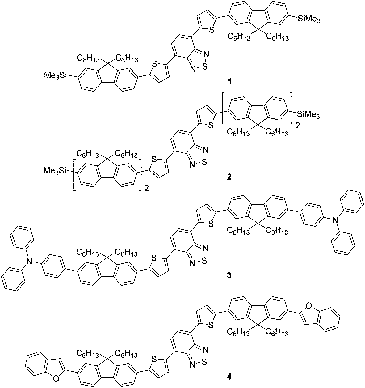 | ||
| Fig. 1 Structures of the molecular emissive species, compounds 1–4. | ||
Results and discussion
Synthesis
The strategy for the synthesis of compounds 1 and 2 is represented in Scheme 1. The construction of the common core unit 7 was achieved in two steps: firstly, 4,7-dibromo-2,1,3-benzothiadiazole (5), which was synthesised according to the literature,26 was coupled with 2-(tributylstannyl)thiophene under Stille conditions to form compound 6.27 Compound 6 was then brominated in the terminal α-positions using N-bromosuccinimide (NBS) to form the key intermediate 7.28 With this in hand, straightforward Suzuki–Miyaura couplings29 with the boronic acid functionalised mono- or bifluorene (8 or 9)30 furnished compounds 1 and 2, respectively. Both reactions proceeded in good yield, giving the target emissive compounds as red powders.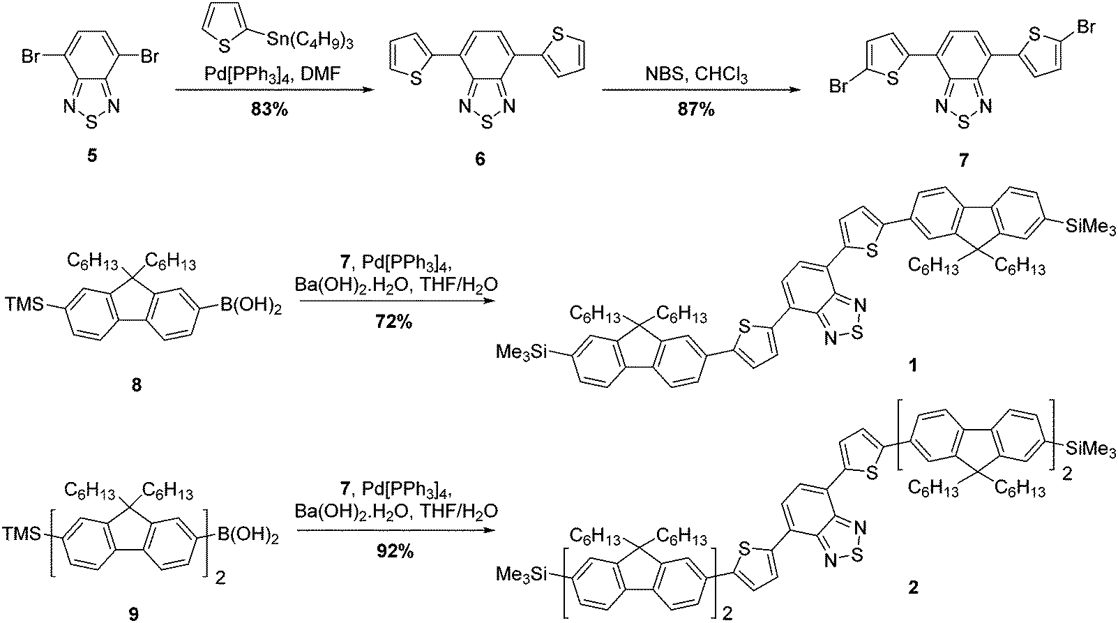 | ||
| Scheme 1 Synthesis of compounds 1 and 2. | ||
The synthesis of compounds 3 and 4 was somewhat more complex (Scheme 2). Our proposed route involved desilylation31 of the terminal trimethylsilyl groups in compound 1 for bromine functionalities (compound 10), followed by Suzuki–Miyaura coupling with the appropriately functionalised terminal group. However, it became clear that substitution of the TMS groups of compound 1 to bromines was challenging, with evidence of over-bromination present regardless of the conditions employed as well as residual TMS groups.‡ Alternative reaction pathways involving iododesilylation32 of the TMS groups were also unsuccessful and led to the formation of by-products. The most successful conditions involved the use of 4.4 equivalents of bromine added to a solution of compound 1 at 0 °C, followed by warming the reaction solution to room temperature overnight. This gave almost quantitative conversion of starting material (97% conversion) with minimal evidence of over-bromination (approximately 6%). As shown in the experimental, exchanging the TMS groups with bromine has no impact on the melting range. The challenging nature of this bromination is in stark contrast to our previous reports using this reaction,20 indicating that the presence of the additional thiophenes is the likely cause of these complications. With compound 10 in hand, albeit as a mixture, Suzuki–Miyaura coupling with the appropriate electron-rich terminal groups afforded compounds 3 and 4 in yields of 63% and 34%, respectively (Scheme 2).
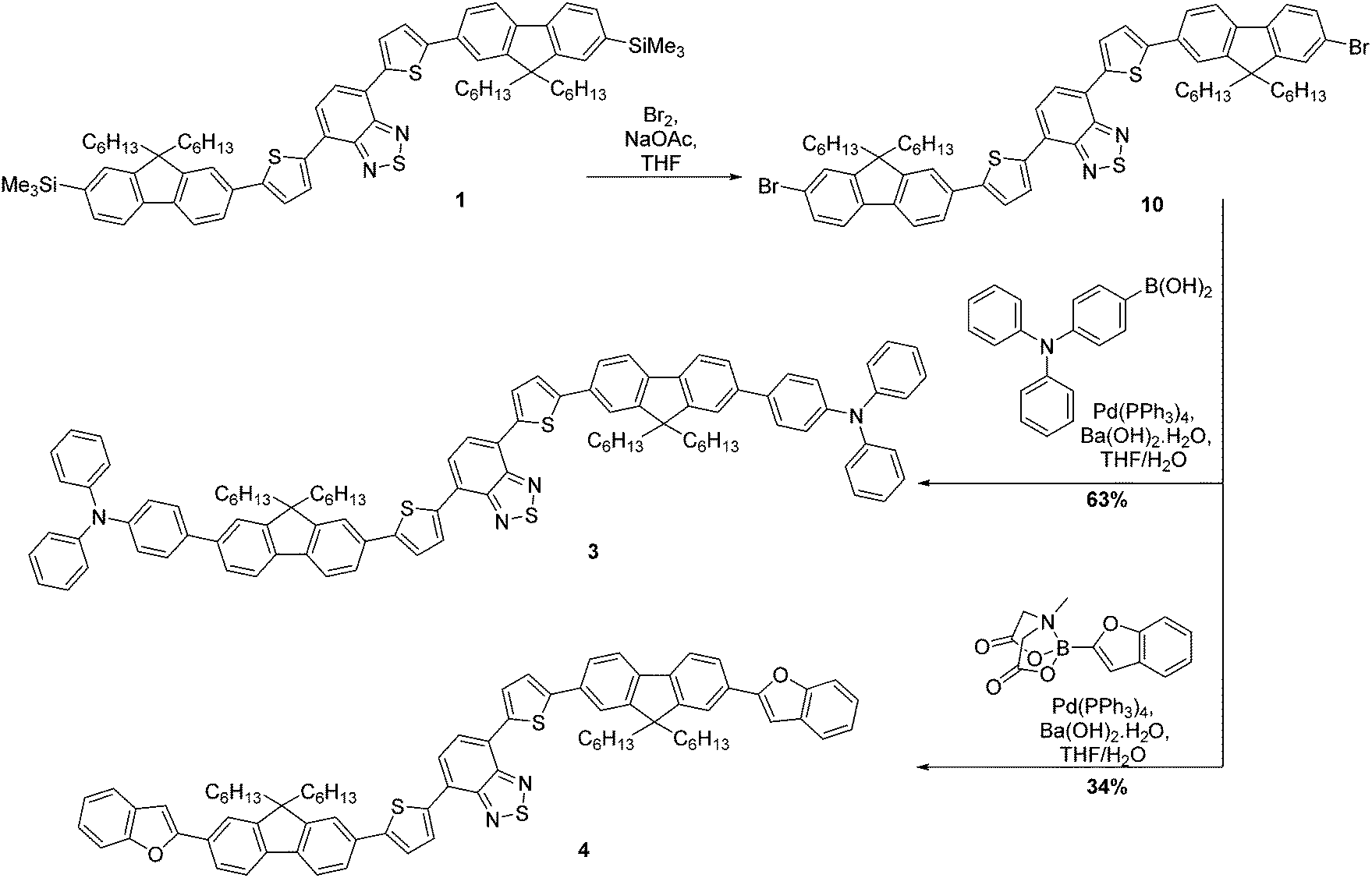 | ||
| Scheme 2 Synthesis of compounds 3 and 4. Note that compound 10 was isolated as a mixture. | ||
Physical characterisation
All compounds within the series show significant thermal stability, with thermal degradation only observed at temperatures above 360 °C (Table 1). Whilst extending the conjugation increased the thermal stability in compound 2 over monofluorene analogue 1, end-capping with either TPA or benzofuran in compounds 3 and 4 offered even more enhanced stability. TPA-containing compound 3 shows the highest thermal stability with a 5% mass loss temperature of 447 °C. Similarly, end-capping significantly altered the type and temperature of the phase changes observed by differential scanning calorimetry (see Table 1). Compounds 1 and 2 recorded glass transition temperatures of 67 °C and 83 °C, respectively. On the contrary, end-capped analogues 3 and 4 showed no transitions at temperatures below 200 °C indicating an increased suitability for device fabrication.| Compound | TGAa [°C] | DSCb [°C] | λ max(abs)c [nm] | λ max(em)c [nm] | E g(opt)d [eV] | PLQYe [%] |
|---|---|---|---|---|---|---|
| a Temperature at which 5% mass loss occurs. b Thermal event recorded by DSC. c Recorded in dichloromethane solution (concentration of 10−5–10−8 M). d Calculated from the onset of the longest wavelength absorbance edge. e Measured from a spin-coated film on a glass substrate at a thickness of 90 nm (±10 nm). | ||||||
| 1 | 361 | 67 (Tg) | 369, 513 | 620 | 2.08 | 19.3 |
| 2 | 391 | 83 (Tg) | 377, 515 | 623 | 2.06 | 32.8 |
| 3 | 447 | 241 (Tm) | 380, 518 | 626 | 2.04 | 31.1 |
| 4 | 408 | 224 (Tm) | 384, 515 | 623 | 2.05 | 23.6 |
UV-Vis absorption analysis in dichloromethane showed distinct similarities across the series, with two major absorption bands and a third low intensity peak at higher energies observed for all compounds, which is neglected in the further discussion (Fig. 2). The short wavelength peaks of higher intensity likely correspond to a π → π* transition of the excitons, while the lower energy band represents a charge-transfer in which the excited electrons remain on the electron-withdrawing benzothiadiazole core, while the holes are delocalised on the fluorene–thiophene moieties.33 Whilst there is little difference across the series in the lower energy band, suggesting that increased electron-donating strength has little effect on the absorption characteristics of the core, a more pronounced bathochromic shift is observed in the higher energy band as the molecular conjugation length is extended in compounds 2–4. Compound 4 offers the largest bathochromic shift compared to compound 1 for the higher energy band, reflecting increased orbital overlap through the planar benzofuran units. On the other hand, the increased donor strength of the TPA groups in compound 3 has a slightly more pronounced effect on the lower energy charge transfer band (Table 1). Similarly, the emission spectra of compounds 1–4 are similar, with one broad band peaking in the range 620–626 nm. The increased donor strength of the TPA units results in the longest wavelength emission maximum of the series for compound 3. Solid-state PLQY values ranging from 19–33% were recorded for the series, with compound 2 proving to be the most efficient emitter (Table 1).
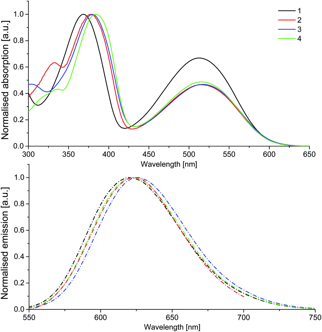 | ||
| Fig. 2 Absorption (top) and emission (bottom) in dichloromethane solution for compounds 1–4. | ||
The effect of extending the conjugation length on the electrochemical behaviour is clear when considering compounds 1 and 2, with a slight increase of the HOMO energy and decrease of the LUMO energy in compound 2 compared to compound 1, resulting in a slight reduction of the electrochemical HOMO–LUMO energy gap (Table 2 and Fig. S1–S4 in the ESI†). Introduction of additional electron-donating groups in compounds 3 and 4 had a subtle effect on the HOMO and LUMO energy levels. Inclusion of the TPA group in compound 3 had no evident effect on the HOMO level compared to compound 1, despite the increase in conjugation length, but reduced the LUMO level to −3.18 eV and the HOMO–LUMO energy gap to 2.06 eV. As observed in the UV-vis absorption spectra, the increased orbital overlap when introducing the planar benzofuran group in compound 4 resulted in a further decrease of the HOMO level to −5.31 eV, while the LUMO level was also reduced when compared to compound 1. However, the overall effect of introducing the benzofuran in compound 4 was an overall widening of the electrochemical HOMO–LUMO energy gap to 2.15 eV. Overall, the electrochemical behaviour of compounds 1–4 does not differ greatly across the series, suggesting that the common thiophene–BT–thiophene core dominates the observed characteristics and that increasing the electron-donor strength within the molecule provides only subtle manipulation of molecular energy levels. This is in contrast to similar green-emitting analogues that do not contain thiophene-based π-spacer groups, as the inclusion of electron-donating functionalities has a significant effect on the molecular energy levels.20
| Compound | Oxidationa,b [V] | Reductiona,b [V] | HOMOa [eV] | LUMOa [eV] | E g [eV] |
|---|---|---|---|---|---|
| a Recorded by cyclic voltammetry of solutions of compounds 1–4 (10−4 M) using glassy carbon, platinum wire and Ag wire as the working, counter and pseudo-reference electrodes, respectively, with (nBu)4NPF6 as the electrolyte in dichloromethane solution (0.1 M), at a scan rate of 100 mV s−1. The data were referenced to the Fc/Fc+ redox couple, which has a HOMO of −4.8 eV. b The peaks shown are anodic/cathodic for oxidation, and cathodic/anodic for reduction waves. c Calculated by subtraction of the HOMO energy from the LUMO energy. d irr = irreversible. | |||||
| 1 | +0.47/+0.42 | −1.71/−1.64 | −5.24 | −3.13 | 2.12 |
| +0.64/+0.60 | −2.20 (irr)d | ||||
| 2 | +0.36/+0.32 | −1.69/−1.62 | −5.14 | −3.15 | 1.99 |
| +0.50/+0.46 | −2.02 (irr)d | ||||
| +0.88/+0.84 | −2.18/−2.12 | ||||
| 3 | +0.47/+0.40 | −1.66/1.59 | −5.24 | −3.18 | 2.06 |
| +0.60/+0.54 | −2.14/−2.05 | ||||
| +0.83/+0.75 | |||||
| 4 | +0.53/+0.48 | −1.67/−1.61 | −5.31 | −3.16 | 2.15 |
| +0.68/+0.62 | −2.14/−2.05 | ||||
OLED fabrication and characterisation
The performance of an OLED is directly influenced by the thickness of the emissive layer;34 defining the optimum thickness early during device optimisation is vital in order to find the balance between a suitably thin active layer for high current, but one that is also thick enough to avoid degradation.35 Compound 1 was initially chosen for concentration optimisation using the device configuration ITO/PEDOT:PSS/compound 1/Ca (40 nm)/Al (60 nm), with compound 1 deposited by spin-coating from toluene solution (Table 3). The impact of the turn on voltage on device performance is clear; an increase of 2 V is observed when the thickness of compound 1 is increased. This is due to the concurrent increase in resistance as the active layer thickness increases.36 This influences the overall luminance of the device as well, with a concentration of 20 mg ml−1 affording an active layer thickness of 90 nm and the highest value for luminance (854 cd m−2). Note that the turn on voltage was recorded when the luminance reached a value of 1 cd m−2.35| Compound | Concentration [mg ml−1] | Turn on voltage [V] (at 1 cd m−2) | Luminance [cd m−2] | Maximum current efficiency [cd A−1] | Maximum EQE [%] |
|---|---|---|---|---|---|
| a Recorded as an average over 8 devices. b Recorded as an average over 6 devices. c Recorded as an average over 5 devices. d Recorded as an average over 3 devices (limited due to short circuits). e Recorded as an average over 5 devices (limited due to short circuits). f Recorded as an average over 4 devices. | |||||
| 1 | 10 | 2.7 | 390@5.8 V | 0.03 | 0.05 |
| 20 | 2.7 (2.8)a | 854@7 V (708@7 V)a | 0.10 (0.093)a | 0.22 (0.19)a | |
| 30 | 4.6 | 343@11.4 V | 0.06 | 0.14 | |
| 2 | 10 | 2.7 | 719@7.2 | 0.06 | 0.08 |
| 20 | 2.9 (3.0)b | 1561@8 V (1410@8 V)b | 0.15 (0.14)b | 0.25 (0.23)b | |
| 30 | 3.3 | 720@9.2 V | 0.16 | 0.19 | |
| 3 (unfiltered) | 10 | 1.9 (2.2)c | 239@20 V (232@19 V)c | 0.012 (0.11)d | 0.03 (0.02)d |
| 20 | 2.1 (2.2)b | 1425@14 V (1238@18 V)b | 0.051 (0.026)b | 0.08 (0.06)b | |
| 30 | 2.1 (2.3)b | 1054@19 V (928@19 V)b | 0.040 (0.24)e | 0.06 (0.05)b | |
| 3 (filtered) | 20 | 2.3 (2.5)a | 2135@8.8 V (1915@9 V)a | 0.086 (0.070)a | 0.16 (0.14)a |
| 10 | 2.2 (2.3)b | 493@5.5 V (421@5.8 V)b | 0.027 (0.022)b | 0.06 (0.05)b | |
| 4 | 20 | 2.5 (2.9)b | 1498@7 V (1079@6.7 V)b | 0.081 (0.064)b | 0.17 (0.13)a |
| 30 | 2.5 (2.7)f | 1003@6.9 V (968@8.1 V)f | 0.073 (0.071)f | 0.15 (0.15) | |
Similarly, compounds 2, 3 and 4 were found to provide optimum OLED performance when processed from solutions of 20 mg ml−1 concentration, with maximum luminance values of 1561, 1425 and 1498 cd m−2, respectively. The higher luminance of compounds 2 and 3 compared with compound 1 can be explained by the higher PLQY (Table 1) values for both compounds compared to the smaller analogue. The extended conjugation present in compounds 2 and 3 recorded a solid state PLQY over 1.5 times higher than compound 1, indicating an increased radiative recombination rate within the material. However, the low current efficiency of compound 3 is unexpected. The main reason that could explain this low efficiency is the roughness of the emissive material surface. Indeed, compared to compounds 1 and 2, compound 3 was less soluble in toluene, resulting in more aggregates and a rougher film. As such, to improve the morphology of the film, the solution of compound 3 in toluene was filtered through a 0.45 μm PTFE filter (see Fig. S5, ESI†). The film quality was largely improved and a uniform film was obtained, resulting in an increased luminance of 2135 cd m−2 and a current efficiency of 0.086 cd A−1, as shown in Table 3. It is likely that by improving the film morphology, fewer charges were trapped by aggregates, resulting in increased numbers reaching the recombination zone. The higher luminance observed for compound 3 can be explained by a higher current passing through the device, as shown in Fig. 3. Additionally, at approximately 7 V for compound 1 and approximately 8 V for compound 2 the current seems to stabilise around 1000 mA cm−2. This saturation phase is not observed in compounds 3 and 4. According to Ohm's law,37 when the voltage is increased, the current should increase proportionally, unless the resistance is changed. For compounds 1 and 2, the resistance of the device increases and the current is limited, while for compounds 3 and 4 no such plateau is evident (Fig. 3).
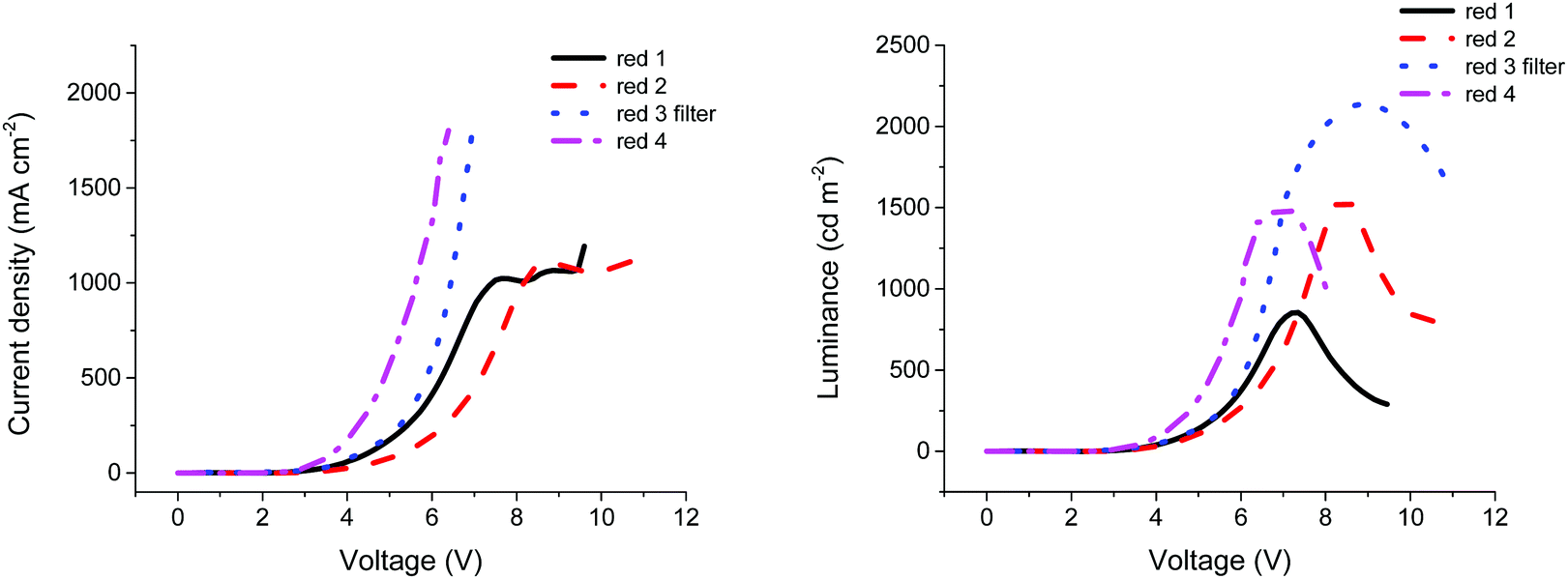 | ||
| Fig. 3 Current density and luminance vs. voltage for compounds 1–4. | ||
Compound 4 offered comparable performance with respect to compounds 2 and 3, with a maximum luminance at 1498 cd m−2 (similar to the luminance of compound 2) whilst the efficiencies of the OLEDs are close to those fabricated with compound 3. However, its slightly reduced overall performance when compared to these two extended conjugated molecules can be explained by the reduced PLQY of compound 4, which could be caused by increased aggregation quenching, possibly due to the presence of planar benzofuran units. Analysis of atomic force microscopy (AFM) topography images (Fig. S6, ESI†) shows that films containing compound 4 are the roughest and contain the largest domain areas which could be caused by increased aggregation with respect to the other materials.
The effect of thermal annealing on the performance of OLEDs containing compounds 1–4 was studied and in general showed no improvement over untreated devices, with only compound 2 showing a small increase in performance with thermal annealing (Table S1, ESI†). For all other devices the maximum luminance and efficiencies dropped upon thermal annealing. Atomic force microscopy images for films annealed at 80 °C (Fig. S7, ESI†) show that the annealing treatment has little effect on the overall topography with images relatively similar to those for the unannealed films (Fig. S6, ESI†) suggesting that decreased performance with annealing is due to subtle morphological changes. In films containing compound 2 annealing results in the root mean square (RMS) roughness being reduced by 0.15 nm. This small reduction in roughness may explain the improved performance with annealing of compound 2 at temperatures below the glass transition temperature (Tg = 83 °C), despite a relatively similar topography overall.
However, since the saturation phase corresponds almost exactly with the voltage at which the maximum luminance was recorded, the peak performance of both compound 1 and compound 2 has not yet been reached. One factor that may cause this is elevated device temperature, with an increase in heat within the device possibly due to inefficient electron injection, particularly at an organo-metal interface.38 To resolve this, an electron-transport layer of tris(8-hydroxyquinolinato)aluminium (Alq3) was thermally deposited on top of the emissive material.39 Compounds 1–4 were investigated alongside Alq3 at two different thicknesses: 20 and 50 nm (Table 4). For each compound, inclusion of a 20 nm layer of Alq3 was detrimental to the maximum luminance, with a drop recorded in each case, while the current efficiency was broadly unaffected. However, inclusion of a thicker layer (50 nm) led to improved devices in every case. Notably compound 3, when filtered as before, offered a maximum luminance of 2888 cd m−2 at a low turn on voltage of just 3.6 V, whilst devices containing compound 2 were most efficient with the highest current efficiency of 0.51 cd A−1 and external quantum efficiency (EQE) of 0.77%. The presence of the peripheral triphenylamino groups on compound 3 likely provides enhanced hole transport,40 leading to better balanced hole and electron transport in the device compared with the other members of the series. However, the Alq3 layer is also contributing to the emission as devices fabricated with 50 nm of Alq3 produced orange light.
| Material | Alq3 thickness [nm] | Turn on [V] (at 1 cd m−2) | Luminance [cd m−2] | Maximum current efficiency [cd A−1] | Maximum EQE [%] |
|---|---|---|---|---|---|
| a Recorded as an average over 8 devices. b Recorded as an average over 4 devices. c Recorded as an average over 6 devices. d Recorded as an average over 3 devices. The best turn on voltages of each compound was recorded without using Alq3. | |||||
| 1 | X | 2.7 (2.8)a | 854@7 V (708@7 V)a | 0.10 (0.093)a | 0.22 (0.19)a |
| 20 | 4.2 (4.5)b | 604@10 V (552@10 V)b | 0.10 (0.098)b | 0.16 (0.16)b | |
| 50 | 5.8 (6.7)b | 1476@12 V (1348@13 V)b | 0.30 (0.28)b | 0.28 (0.27)b | |
| 2 | X | 2.9 (3.0)c | 1561@8 V (1410@8 V)c | 0.15 (0.14)c | 0.25 (0.23)b |
| 20 | 4.2 (4.9)d | 1287@11 (1143@10.6 V)d | 0.17 (0.14)d | 0.25 (0.23)d | |
| 50 | 6.5 (7.5)b | 2640@13 V (2483@12 V)b | 0.51 (0.44)b | 0.77 (0.69)b | |
| 3 (filtered) | X | 2.3 (2.5)a | 2135@8.8 V (1915@9 V)a | 0.086 (0.070)a | 0.16 (0.14)a |
| 20 | 3.8 (3.9)d | 1862@10 V (1547@10 V)d | 0.11 (0.10)d | 0.22 (0.21)d | |
| 50 | 3.6 (3.8)b | 2888@10 V (2584@10 V)b | 0.30 (0.26)b | 0.46 (0.41)b | |
| 4 | X | 2.5 (2.9)a | 1498@7 V (1079@6.7 V)a | 0.081 (0.064)a | 0.17 (0.13)a |
| 20 | 3.6 (3.6)b | 1441@8.5 V (1241@8.1 V)b | 0.089 (0.083)b | 0.17 (0.15)b | |
| 50 | 3.6 (3.6)d | 1572@8.6 V (1457@8.4 V)d | 0.16 (0.12)d | 0.25 (0.18)d | |
Conclusion
Herein, a series of four linear, solution-processable red emissive molecules have been reported, all containing a thiophene–benzothiadiazole–thiophene core. The molecules differ through the extent of conjugation and choice of end group functionalisation, which although offering little difference in the physical characteristics of the series, led to significant differences in OLED performance. Compound 3, containing peripheral triphenylamine groups exhibited the highest maximum luminance of 2135 cd m−2 in addition to a low turn on voltage of 2.3 V when used in a device configuration of ITO/PEDOT:PSS/compound 3/Ca/Al. However, the most efficient OLED in this configuration was produced when compound 2 was the emissive component, leading to an EQE of 0.25%. This trend was consistent when a 50 nm layer of Alq3 led to increased luminance in the compound 3 containing device (2888 cd m−2), and highest efficiency when compound 2 was used (0.77%). The dual emission of the red material and green light from Alq3 led to the production of orange light. Such straightforward, readily prepared molecules could be considered as inexpensive fluorescent orange OLEDs for tandem white light devices.Experimental
General
Tetrakis(triphenylphosphine)palladium(0) (Pd(PPh3)4) was prepared41 prior to use and stored under nitrogen. 4,7-Dibromobenzothiadiazole26 and 9,9-dihexyl-7-trimethylsilylfluoren-2-ylboronic acid and its derivative with two fluorene moieties (compound 8 and 9)30 were synthesised according to the literature. Unless otherwise stated, all other reagents were sourced commercially and used without further purification. Dry solvents were obtained from a solvent purification system (SPS 400 from Innovative Technologies) using alumina as the drying agent. 1H and 13C nuclear magnetic resonance (NMR) spectra were recorded on either a Bruker DRX 500 apparatus at 500.13 and 125.76 MHz, or a Bruker Avance DPX400 apparatus at 400.13 and 100.6 MHz. Chemical shifts are given in ppm; all J values are in Hz. Elemental analyses were obtained on a PerkinElmer 2400 analyser. Matrix assisted laser desorption ionisation-time-of-flight (MALDI-TOF) mass spectrometry were run on a Shimadzu Axima-CFR spectrometer (mass range 1–150000 Da). Thermogravimetric analysis (TGA) was performed using a PerkinElmer Thermogravimetric Analyzer TGA7 under a constant flow of argon. Differential scanning calorimetry (DSC) was recorded on a TA Instruments DSC QC1000 under nitrogen gas. Melting points were taken using a Stuart Scientific Melting Point apparatus. Absorption spectra were recorded on a Shimadzu UV 2700 instrument. Atomic force microscopy studies were carried out using a Bruker Innova AFM and the data was processed using the NanoScope Analysis 1.5 program by Bruker. Photoluminescence measurements were recorded using a PerkinElmer LS 50 B fluorescence spectrometer in a quartz cuvette (path length 10 mm). Absolute PLQY measurements were performed in a calibrated integrating sphere42 attached to an Ocean Optics USB2000+ spectrometer, and a Gooch & Housego double monochromater with a quartz halogen lamp. The samples were excited at their corresponding longest absorption wavelength. Cyclic voltammetry was recorded on a CH Instruments 660A electrochemical workstation with iR compensation at a scan rate of 100 mV s−1 using anhydrous dichloromethane as the solvent. The electrodes were glassy carbon, platinum wire and silver wire as the working, counter and pseudo-reference electrodes, respectively. All solutions were degassed (Ar) and contained monomer substrates in concentrations of ca. 10−4 M, together with 0.1 M tetrabutylammonium hexafluorophosphate as the supporting electrolyte. All measurements were referenced against the E1/2 of the Fc/Fc+ redox couple. The HOMO (LUMO) was calculated by subtracting the half-wave potential of oxidation (reduction) from −4.8 eV.43
Pre-patterned ITO slides (7 Ω sq−1, 15 mm × 15 mm × 1.1 mm, KINTEC) were cleaned with deionised water, acetone and isopropanol in an ultrasonic bath before treatment with UV–ozone for 2 minutes. This method has been shown to improve the hole injection of ITO and the performance of devices in general.44 PEDOT:PSS (Heraeus P VP AL 4083) was spin-coated onto the pre-cleaned ITO substrates at 3000 rpm and annealed at 120 °C for 20 minutes, before cooling to room temperature. These substrates were transferred into a glove box where all the subsequent fabrications and measurements were performed. Solutions of compounds 1–4 were prepared using toluene with varying concentrations of 10, 20 and 30 mg ml−1. For compound 1, a solution concentration of 20 mg ml−1 was found to be optimum and hence used to continue other characterisation measurements such as annealing. These spin-coated films were annealed for 10 minutes at temperatures of 40, 60 and 80 °C. After annealing these films were transferred into a thermal evaporator attached to the glove box for evaporation of the electrodes. An active area of 1.5 × 3.5 mm2 was obtained by evaporation of 40 nm of calcium and 40 nm of aluminium electrodes through a shadow mask at the base pressure of 1 × 10⁻⁶ mbar. JVL were measured inside the glove box with a light-tight box attached. A Keithley Semiconductor Characterisation (SCS) 4200 was used to bias the OLEDs. Luminance measurements were performed by using a Macom L203 photometer with a calibrated silicon photodetector and a photopic filter. These calibrations can be traced back to the National Physical Laboratory, London standards. Wavelength dependent electroluminescence spectra were measured by using an Ocean optics USB2000+ spectrometer under a lab atmosphere.
:3). Re-precipitation in methanol gave a red solid, which was then washed with acetone, resulting in isolation of the product (3) as an orange solid (0.200 g, 63%) after drying in a desiccator; δH (CDCl3, 400.13 MHz) 8.17 (2H, d, J 3.9 Hz, ArH), 7.96 (2H, s, ArH), 7.78–7.70 (6H, m, ArH), 7.67 (2H, s, ArH), 7.61–7.53 (8H, m, ArH), 7.51 (2H, d, J 3.9 Hz, ArH), 7.28 (8H, t, J 8.3 Hz, ArH), 7.17 (12H, t, J 8.4 Hz, ArH), 7.05 (4H, t, J 7.5 Hz, ArH), 2.06 (8H, m, CH2), 1.19–0.98 (24H, m, CH2), 0.80–0.67 (20H, m, CH2, CH3); δC (CDCl3, 100.76 MHz) 152.8, 152.0, 151.8, 147.8, 147.3, 146.7, 141.0, 139.9, 139.6, 138.5, 135.7, 132.9, 129.4, 128.8, 127.9, 126.0, 125.8, 125.4, 125.0, 124.5, 124.2, 123.1 121.0, 120.2, 55.5, 40.7, 31.6, 29.8, 24.0, 22.7, 14.2; m/z (MALDI-TOF) 1450.39; HRMS calculated for C100H98N4S3: (M + H)+, 1451.7032. Found: 1451.7015; TGA: 5% mass loss at 447 °C; Tm (DSC) = 241 °C; m.p. 240–242 °C.
:3) as eluent, while the second used petroleum ether 40–60 °C: CHCl3 (8:2). The product was further purified by re-precipitation in methanol. Following drying in a desiccator, the desired product (4) was isolated as a red powder (0.105 g, 34%); δH (CDCl3, 400.13 MHz) 8.17 (2H, J 3.9 Hz, ArH), 7.97 (2H, s, ArH), 7.90–7.84 (4H, m, ArH), 7.78 (2H, d, J 8.2 Hz, ArH), 7.76–7.72 (4H, m, ArH), 7.69 (2H, s, ArH), 7.61 (2H, d, J 7.6 Hz, ArH), 7.58 (2H, d, J 8.1 Hz, ArH), 7.54 (2H, d, J 3.9, ArH), 7.31 (2H, td, J 15.2, 7.0, 1.2 Hz, ArH), 7.25,§ 7.12 (2H, s, ArH), 2.10 (8H, m, CH2), 1.19–1.01 (24H, m, CH2), 0.75 (12H, J 6.97 Hz, CH3), 0.68 (8H, m, CH2); δC (CDCl3, 100.76 MHz) 156.7, 155.1, 152.8, 152.1, 151.8, 146.5, 141.3, 140.7, 138.6, 133.3, 129.6, 129.5, 128.8, 125.9, 125.5, 125.1, 124.3, 124.3, 124.2, 123.1, 120.9, 120.5, 120.3, 120.2, 119.3, 111.3, 101.4, 55.6, 40.6, 31.6, 29.8, 24.0, 22.6, 14.2; m/z (MALDI-TOF) 1196.15; HRMS calculated for C80H80N2O2S3: (M + H)+, 1197.5455. Found: 1197.5450; TGA: 5% mass loss at 408 °C; Tm (DSC) = 224 °C, m.p. 232–234 °C.
Conflicts of interest
There are no conflicts of interest to declare.Acknowledgements
NJF, JC and AK thank the EPSRC for funding (EP/R03480X/1, EP/P02744X/2 and EP/N009908/2). We acknowledge the EPSRC UK National Mass Spectrometry Facility (NMSF) at Swansea University for HRMS data.References
- C. W. Tang and S. A. VanSlyke, Appl. Phys. Lett., 1987, 51, 913–915 CrossRef CAS.
- Y. R. Cho, H. S. Kim, Y. J. Yu and M. C. Suh, Sci. Rep., 2015, 5, 15903 CrossRef CAS PubMed.
- L. Duan, L. Hou, T.-W. Lee, J. Qiao, D. Zhang, G. Dong, L. Wang and Y. Qiu, J. Mater. Chem., 2010, 20, 6392–6407 RSC.
- A. C. Grimsdale, K. Leok Chan, R. E. Martin, P. G. Jokisz and A. B. Holmes, Chem. Rev., 2009, 109, 897–1091 CrossRef CAS.
- M. Zhu and C. Yang, Chem. Soc. Rev., 2013, 42, 4963–4976 RSC.
- A. L. Kanibolotsky, I. F. Perepichka and P. J. Skabara, Chem. Soc. Rev., 2010, 39, 2695–2728 RSC.
- A. A. Zakhidov, J.-K. Lee, H. H. Fong, J. A. DeFranco, M. Chatzichristidi, P. G. Taylor, C. K. Ober and G. G. Malliaras, Adv. Mater., 2008, 20, 3481–3484 CrossRef CAS.
- J.-K. Lee, M. Chatzichristidi, A. A. Zakhidov, P. G. Taylor, J. A. DeFranco, H. S. Hwang, H. H. Fong, A. B. Holmes, G. G. Malliaras and C. K. Ober, J. Am. Chem. Soc., 2008, 130, 11564–11565 CrossRef CAS PubMed.
- K. S. Yook and J. Y. Lee, Adv. Mater., 2014, 26, 4218–4233 CrossRef CAS PubMed.
- T. M. Eggenhuisen, Y. Galagan, A. F. K. V. Biezemans, T. M. W. L. Slaats, W. P. Voorthuijzen, S. Kommeren, S. Shanmugam, J. P. Teunissen, A. Hadipour, W. J. H. Verhees, S. C. Veenstra, M. J. J. Coenen, J. Gilot, R. Andriessen and W. A. Groen, J. Mater. Chem. A, 2015, 3, 7255–7262 RSC.
- T. M. Eggenhuisen, Y. Galagan, E. W. C. Coenen, W. P. Voorthuijzen, M. W. L. Slaats, S. A. Kommeren, S. Shanmuganam, M. J. J. Coenen, R. Andriessen and W. A. Groen, Sol. Energy Mater. Sol. Cells, 2015, 134, 364–372 CrossRef CAS.
- H. Xu, R. Chen, Q. Sun, W. Lai, Q. Su, W. Huang and X. Liu, Chem. Soc. Rev., 2014, 43, 3259–3302 RSC.
- D. Chen, X. Cai, X.-L. Li, Z. He, C. Cai, D. Chen and S.-J. Su, J. Mater. Chem. C, 2017, 5, 5223–5231 RSC.
- P. Data, P. Pander, M. Okazaki, Y. Takeda, S. Minakata and A. P. Monkman, Angew. Chem., Int. Ed., 2016, 55, 5739–5744 CrossRef CAS PubMed.
- Y. Wong Michael and E. Zysman-Colman, Adv. Mater., 2017, 29, 1605444 CrossRef.
- M. Shimizu, R. Kaki, Y. Takeda, T. Hiyama, N. Nagai, H. Yamagishi and H. Furutani, Angew. Chem., Int. Ed., 2012, 51, 4095–4099 CrossRef CAS PubMed.
- T. Khanasa, N. Prachumrak, R. Rattanawan, S. Jungsuttiwong, T. Keawin, T. Sudyoadsuk, T. Tuntulani and V. Promarak, Chem. Commun., 2013, 49, 3401–3403 RSC.
- N. Prachumrak, S. Pojanasopa, S. Namuangruk, T. Kaewin, S. Jungsuttiwong, T. Sudyoadsuk and V. Promarak, ACS Appl. Mater. Interfaces, 2013, 5, 8694–8703 CrossRef CAS PubMed.
- L. Yao, S. Zhang, R. Wang, W. Li, F. Shen, B. Yang and Y. Ma, Angew. Chem., Int. Ed. Engl., 2014, 53, 2119–2123 CrossRef CAS PubMed.
- N. J. Findlay, B. Breig, C. Forbes, A. R. Inigo, A. L. Kanibolotsky and P. J. Skabara, J. Mater. Chem. C, 2016, 4, 3774–3780 RSC.
- M. Sims, D. D. C. Bradley, M. Ariu, M. Koeberg, A. Asimakis, M. Grell and D. G. Lidzey, Adv. Funct. Mater., 2004, 14, 765–781 CrossRef CAS.
- P. Sonar, R. Y. C. S. K. Sien, Z. Chen, K. H. Ong, G. M. Ng and A. Zen, US Pat., US2012/0298976A1, 2012 Search PubMed.
- Z. Zhao and V. Snieckus, Org. Lett., 2005, 7, 2523–2526 CrossRef CAS PubMed.
- N. Cho, K. Song, K. Lee Jae and J. Ko, Chem. – Eur. J., 2012, 18, 11433–11439 CrossRef CAS PubMed.
- A. Yassin, P. Leriche, M. Allain and J. Roncali, New J. Chem., 2013, 37, 502–507 RSC.
- B. A. DaSilveira Neto, A. Sant'Ana Lopes, G. Ebeling, R. S. Gonçalves, V. E. U. Costa, F. Quina and J. Dupont, Tetrahedron, 2005, 61, 10975–10982 CrossRef CAS.
- J. F. Lee, L. C. Hsu Steve, I. Lee Po, H. Y. Chuang, J. S. Chen and W. Y. Chou, J. Polym. Sci., Part A: Polym. Chem., 2011, 49, 4618–4625 CrossRef CAS.
- Y. Jeon, T.-M. Kim, J.-J. Kim and J.-I. Hong, New J. Chem., 2015, 39, 9591–9595 RSC.
- N. Miyaura and A. Suzuki, Chem. Rev., 1995, 95, 2457–2483 CrossRef CAS.
- C. R. Belton, A. L. Kanibolotsky, J. Kirkpatrick, C. Orofino, S. E. T. Elmasly, P. N. Stavrinou, P. J. Skabara and D. D. C. Bradley, Adv. Funct. Mater., 2013, 23, 2792–2804 CrossRef CAS.
- M. Tavasli, S. Bettington, M. R. Bryce, H. A. A. Attar, F. B. Dias, S. King and A. P. Monkman, J. Mater. Chem., 2005, 15, 4963–4970 RSC.
- D. Hoppe and M. Kauch, Synthesis, 2006, 1578–1589 CrossRef.
- K. G. Jespersen, W. J. D. Beenken, Y. Zaushitsyn, A. Yartsev, M. Andersson, T. Pullerits and V. Sundström, J. Chem. Phys., 2004, 121, 12613–12617 CrossRef CAS PubMed.
- S. Höfle, T. Lutz, A. Egel, F. Nickel, S. W. Kettlitz, G. Gomard, U. Lemmer and A. Colsmann, ACS Photonics, 2014, 1, 968–973 CrossRef.
- C. C. Yap, M. Yahaya and M. M. Salleh, Curr. Appl. Phys., 2008, 8, 637–644 CrossRef.
- T. Taima, M. Chikamatsu, Y. Yoshida, K. Saito and K. Yase, Appl. Phys. Lett., 2004, 85, 6412–6414 CrossRef CAS.
- A. Métioui, C. Brassard, J. Levasseur and M. Lavoie, Int. J. Sci. Educ., 1996, 18, 193–212 CrossRef.
- K. Kwak, K. Cho and S. Kim, Opt. Express, 2013, 21, 29558–29566 CrossRef PubMed.
- C. Y. Kwong, A. B. Djurišić, W. C. H. Choy, D. Li, M. H. Xie, W. K. Chan, K. W. Cheah, P. T. Lai and P. C. Chui, Mater. Sci. Eng., B, 2005, 116, 75–81 CrossRef.
- Y. Yang, J. Zhang, Y. Zhou, G. Zhao, C. He, Y. Li, M. Andersson, O. Inganäs and F. Zhang, J. Phys. Chem. C, 2010, 114, 3701–3706 CrossRef CAS.
- D. R. Coulson, L. C. Satek and S. O. Grim, Inorg. Synth., 1972, 13, 121 Search PubMed.
- J. C. de Mello, H. F. Wittmann and R. H. Friend, Adv. Mater., 1997, 9, 230–232 CrossRef CAS.
- A. L. Kanibolotsky, N. J. Findlay and P. J. Skabara, Beilstein J. Org. Chem., 2015, 11, 1749–1766 CrossRef CAS PubMed.
- C. C. Wu, C. I. Wu, J. C. Sturm and A. Kahn, Appl. Phys. Lett., 1997, 70, 1348–1350 CrossRef CAS.
- C. Kitamura, S. Tanaka and Y. Yamashita, Chem. Mater., 1996, 8, 570–578 CrossRef CAS.
- Z. Zhao, C. Deng, S. Chen, J. W. Y. Lam, W. Qin, P. Lu, Z. Wang, H. S. Kwok, Y. Ma, H. Qiu and B. Z. Tang, Chem. Commun., 2011, 47, 8847–8849 RSC.
- C. Shi, Y. Wu, W. Zeng, Y. Xie, K. Yang and Y. Cao, Macromol. Chem. Phys., 2005, 206, 1114–1125 CrossRef CAS.
Footnotes |
| † Electronic supplementary information (ESI) available: The graphs for the oxidation and reduction CV cycles of compounds 1–4 are shown in the ESI in Fig. S1–S4, as well as the optical microscope images in Fig. S5, AFM images of unannealed films and films annealed at 80 °C in Fig. S6 and S7 respectively, OLED data at various annealing temperatures of compound 1–4 in Table S1 and 1H and 13C NMR spectra for compounds 1–4 in Fig. S8–S15. Supporting data are accessible from http://dx.doi.org/10.5525/gla.researchdata.622. See DOI: 10.1039/c8tc02993h |
| ‡ 1H NMR and MALDI analysis of the isolated mixture identified peaks corresponding to the presence of TMS groups and excess bromination. Separation of the mixture was challenging and the next synthetic step was undertaken without further purification. |
| § Integration not possible due to overlap with CDCl3 peak. Use of CD2Cl2 not suitable due to aggregation causing broad signals. |
| This journal is © The Royal Society of Chemistry 2019 |