 Open Access Article
Creative Commons Attribution 3.0 Unported Licence
Correction: Significant average ZT enhancement in Cu3SbSe4-based thermoelectric material via softening p–d hybridization
Dan
Zhang
ab,
Junyou
Yang
*b,
Hongchang
Bai
a,
Yubo
Luo
c,
Bin
Wang
a,
Shuaihang
Hou
a,
Zhiliang
Li
*a and
Shufang
Wang
*a
aHebei Key Lab of Optic-Electronic Information and Materials, The College of Physics Science and Technology, Hebei University, Baoding 071002, P. R. China. E-mail: phd-lzl@hbu.edu.cn; sfwang@hbu.edu.cn
bState Key Laboratory of Material Processing and Die & Mould Technology, Huazhong University of Science & Technology, Wuhan 430074, P. R. China. E-mail: jyyang@mail.hust.edu.cn
cSchool of Materials Science and Engineering, Nanyang Technological University, 50 Nanyang Avenue, 639798, Singapore
First published on 15th July 2019
Abstract
Correction for ‘Significant average ZT enhancement in Cu3SbSe4-based thermoelectric material via softening p–d hybridization’ by Dan Zhang et al., J. Mater. Chem. A, 2019, DOI: 10.1039/c9ta05115e.
The authors regret the following errors in the labelling of Cu and Ag orbitals in the published article:
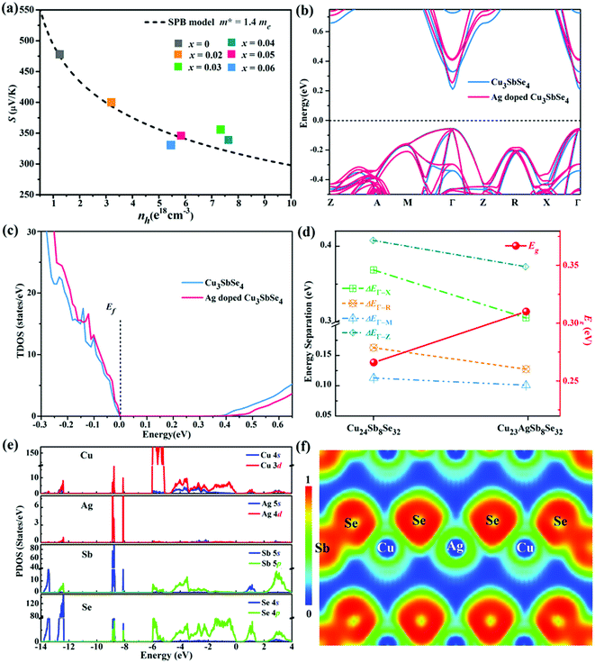
In the Results and discussion section, the text “The calculated partial density of states (PDOS) for pristine Cu3SbSe4 (Fig. S3†) shows the valence band is dominated by strong hybridization between Cu 4d orbitals and Se 4p orbitals, whereas the conduction band edge is mainly formed of Sb 5s orbitals and p orbitals of neighboring Se. As Ag 5d orbitals are located at much lower energies (Fig. 4e)…” should instead read as follows: “The calculated partial density of states (PDOS) for pristine Cu3SbSe4 (Fig. S3†) shows the valence band is dominated by strong hybridization between Cu 3d orbitals and Se 4p orbitals, whereas the conduction band edge is mainly formed of Sb 5s orbitals and p orbitals of neighboring Se. As Ag 4d orbitals are located at much lower energies (Fig. 4e)…”
In Fig. 4e, the labels ‘Cu 4d’ and ‘Ag 5d’ should instead read ‘Cu 3d’ and ‘Ag 4d’, respectively. A corrected version of Fig. 4 is provided below.
In the originally published version of Fig. S3, the label ‘Cu 4d’ should instead have read ‘Cu 3d’. This error has now been corrected in the ESI which is available online.
The Royal Society of Chemistry apologises for these errors and any consequent inconvenience to authors and readers.
| This journal is © The Royal Society of Chemistry 2019 |

