DOI:
10.1039/C9TA10128D
(Paper)
J. Mater. Chem. A, 2019,
7, 27124-27134
Suppression of thermal conductivity without impeding electron mobility in n-type XNiSn half-Heusler thermoelectrics†
Received
13th September 2019
, Accepted 14th November 2019
First published on 19th November 2019
Abstract
We outline a strategy to improve the thermoelectric performance of n-type XNiSn based half-Heusler alloys through Cu doping into vacant tetrahedral sites. A comprehensive combination of structural characterisation and modelling is employed to discriminate the competing mechanisms for thermoelectric enhancement. During synthesis a mineralising effect occurs that improves the homogeneity of the alloying elements Ti, Zr and Hf, and promotes grain growth, leading to a doubling of the electron mobility. In the formed materials, Cu is a strong n-type dopant, like Sb, but occupies the interstitial site and strongly enhances phonon scattering without diminishing carrier mobility (in contrast to interstitial Ni). Simultaneous alloying with Ti, Zr and Hf serves to minimise the thermal conductivity via regular mass disorder and strain effects. A best electronic power factor, S2/ρ, of 3.6 mW m−1 K−2 and maximum ZT of 0.8 at 773 K were observed for a Ti0.5Zr0.25Hf0.25NiCu0.025Sn composition, enabling promising device power densities of ∼6 W cm−2 and ∼8% conversion efficiency from a 450 K gradient. These findings are important because they provide new insight into the mechanisms underpinning high ZT in the XNiSn system and indicate a direction for further improvements in thermoelectric performance.
Introduction
Thermoelectric generators are a renewable energy technology that can increase the efficiency of power generation and usage.1,2 However, widespread application has been limited by the availability of high-performing materials that also satisfy the engineering requirements resulting from harvesting heat. Half-Heuslers (HHs) present arguably the best compromise between good thermoelectric efficiencies, temperature stability, mechanical properties, scalability and use of relatively abundant non-toxic elements.3–6 HH p-types have been developed rapidly over the past 5 years with thermoelectric figures of merit around ZT ∼ 1.5 reported for X′FeSb (X′ = Nb, Ta) and ZrCoBi-based compositions.7–12 By contrast, the long-established n-type XNiSn compositions (X = Ti, Zr, Hf) have proved more difficult to optimise with ZT just over a value of 1,13–15 and possibly as high as ZT ∼ 1.5.16 Here, ZT = (S2/ρκ)T, where S is the Seebeck coefficient, ρ is the electrical resistivity, κ is the sum of the lattice (κlat) and electronic (κel) thermal conductivities, T is the absolute temperature and ZT is the preferred figure of merit because it is dimensionless.
In general, HHs are characterised by large power factors, S2/ρ, and are limited by relatively large κlat values. Most attention has therefore focused on finding new routes to enhance phonon scattering in these materials. The main route has been alloying with isovalent elements, leaving the electrical properties largely unaffected.17 Other successful routes are to enhance boundary scattering through reduction of the average grain size18–20 and by exploiting out-of-equilibrium approaches and segregation to create nanostructured materials.21–40 We have demonstrated that TiNiSn is unique in its ability to accommodate significant amounts of interstitial Ni and Cu metals (∼10% site occupancy),41–44 whereas ZrNiSn and HfNiSn have far lower capacities (<2–3%) under the same preparation conditions.45 These interstitials form highly effective phonon scattering centres, e.g. κlat ∼ 4.5 W m−1 K−1 for ∼5% interstitial site occupancy, with a much stronger impact than expected from alloy phonon scattering only.43,46 In addition, Cu interstitials are effective n-type dopants and lead to rapid S2/ρ improvements, enabling ZT = 0.6 at 773 K and commercially viable power outputs.43 However, our previous study did not address the impact of interstitial Cu on the electron mobility. A further benefit of using excess Cu is that it we have found it to reside as coherent metallic ‘wetting layers’ at grain boundaries after hot-pressing, which appears to reduce grain boundary resistances.43
This manuscript addresses the question of the impact of the combined use of X-site alloying and interstitial metals in the Ti0.5Zr0.25Hf0.25NiCuySn system. The X-site composition was chosen to afford large mass and size disorder and corresponds to ratios used in studies reporting high ZT values.15,16,21,22 An interstitial range of 0 ≤ y ≤ 0.075 was chosen as this covers the range of useful n-type doping and reduction of κlat for the TiNiCuySn series. We have used extensive characterisation including synchrotron X-ray, neutron powder diffraction, scanning and transmission electron microscopies and spectroscopies, thermoelectric property and Hall measurements, single parabolic band modelling and density functional calculations. These give new insights into the atomic-scale structure and microstructures and the impact on the electrical and thermal transport, providing new guidance to develop strategies for optimising thermoelectric performance in HH materials. A highest ZT of 0.8 at 773 K was observed, enabling a ∼6 W cm−2 leg power output with ∼8% efficiency. In terms of overall performance, the main impact of alloying is an increase in efficiency (from ∼6%), while the estimated power output is similar (6–7 W cm−2 without alloying). The analysis suggests that further improvements in performance, approaching the state-of-the-art, are possible with improvements to sample microstructure and homogenisation, making this a compelling materials system for commercial exploitation.
Experimental
Synthesis
Samples with composition Ti0.5Zr0.25Hf0.25NiCuySn (y = 0, 0.025, 0.05 and 0.075) with masses of 5 g were prepared by solid-state reaction of elemental powders purchased from Alfa Aesar of >99.5% purity. The elemental powders were mixed using an agate pestle and mortar, then cold pressed into 13 mm diameter disks. These disks were wrapped in tantalum foil, sealed in an evacuated silica ampoule and sintered at 1123 K for 24 hours. The disks were then reground, repressed, resealed and annealed for 1123 K for 14 days. For the purposes of property measurement, the samples were then hot pressed for 20 minutes under an argon atmosphere, using an applied pressure of 80 MPa and temperature of 1173 K, yielding near theoretical densities for the Cu containing samples. Note that two additional samples were prepared for the Hall measurements (y = 0.0125 and y = 0.0375) using an identical route.
Powder diffraction
Samples were initially characterised using powder X-ray diffraction (XRD). Data were collected over 8 hours using a Bruker D8 Advance diffractometer with monochromated Cu Kα1 radiation. Room temperature neutron powder diffraction (NPD) data from 1–2 g of finely ground powders were collected using the Polaris instrument at the ISIS facility, Rutherford Appleton Laboratory, UK. Rietveld refinement of NPD data was performed using the General Structure Analysis System (GSAS) and its user interface EXPGUI.47,48 Synchrotron X-ray diffraction (SXRD) data (λ = 0.825921 Å, step size 0.002°) were collected on the high-resolution powder diffractometer beamline I11 at the Diamond Light Source, UK. Rietveld refinement of the SXRD data were performed using the TOPAS Academic software package and input file editor jEdit.49
Microscopy
A Thermo Fischer Helios Dualbeam microscope was used to analyse the mechanically-polished surfaces of cut ingots by Scanning Electron Microscopy (SEM). It was also equipped with a Bruker XFlash 100 mm2 detector that was used for energy dispersive X-ray spectroscopy (EDS) compositional analysis. A Bruker eFlash FS electron back-scattered diffraction (EBSD) detector was used to assess the granularity of samples, with Bruker ESPRIT software indexing the EBSD patterns, mapping the crystallographic orientation across the exposed sample surface and ATOM50 software generating grain boundary reconstructions. Scanning transmission electron microscopy (STEM) was performed on a JEOL ARM instrument operated at 200 keV and equipped with a cold field emission gun. Electron energy loss spectroscopy (EELS) datasets were acquired using the Spectrum Imaging (SI) methodology51 with a Gatan Quantum spectrometer and typically alongside high angle annular dark field (HAADF) images. Analysis of EELS spectra was performed using DigitalMicrograph software: SI spectra were aligned by their zero-loss-peak, de-noised by X-rays/artefact spikes removal then using principal component analysis, deconvolved to remove plural scattering effects, background-subtracted, analysed using the cross-sectional data within DigitalMicrograph and finally low-pass filtered to produce atomic-resolved elemental maps.
Thermoelectric properties
The electrical resistivity (ρ) and Seebeck coefficient (S) were measured on bar-shaped specimens (∼1.5 × 2 × 10 mm3) between 313 K and 773 K in a He atmosphere using a Linseis LSR-3 instrument. The thermal diffusivity (α) was measured using disks of ∼13 mm diameter and ∼1.5 mm thickness between 323 K and 773 K under vacuum using a Linseis LFA-1000 instrument. The disks were coated using a carbon spray to reduce error in emissivity. The heat capacity, Cp(T), of Ti0.5Zr0.25Hf0.25NiSn was measured using a PerkinElmer DSC 8500 instrument. Hall measurements were taken using the method of van der Pauw using a magnetic field of ±1 T and a DC current of ≤±100 mA, leading to Hall voltages of ±0.1–10 mV, measured using a nanovoltmeter. Silver paint was used to make contacts on the corners of ∼5 × 5 × 1.5 mm3 squares, which were clamped into a probe card for measurement.
DFT calculations
Electronic structure calculations were performed using the CASTEP first principles simulation package.52 The supercell approximation was used with 2 × 2 × 2 multiples of the primitive cell (fcc) of stoichiometric TiNiSn, containing 24 atoms to model the Ti0.5Zr0.5NiSn composition and 1 additional atom filling a vacancy site for compositions with interstitials: the equivalent of 0.125 excess Ni or Cu. Calculations used the PBE53 general gradient approximation treatment of the exchange-correlation functional and an ultrasoft pseudopotential set, which was generated on the fly using CASTEP version 18.1. Convergence parameters for the plane-wave cut off were determined to be in the range of 600–800 eV and the sampling was performed on a 4 × 4 × 4 Monkhorst–Pack k-point sampling grid. This corresponds to a total energy convergence of 0.5 meV atom−1 or better. Structural relaxation was performed using the LBFGS optimization method as implemented in CASTEP. The force and stress convergence for the geometry optimisation were 0.03 eV Å−1 and 0![[thin space (1/6-em)]](https://www.rsc.org/images/entities/char_2009.gif) :05 GPa respectively. The electronic band structures were unfolded onto the primitive cell using the bs_sc2pc code,54 which implements the scheme described by Popescu and Zunger,55 modified for use with ultrasoft pseudopotentials. The effective band structure for the relaxed structure was calculated along the Γ – X – Γ – L – W – X path in the primitive Brillouin zone using the same convergence parameters as for the structural relaxation.
:05 GPa respectively. The electronic band structures were unfolded onto the primitive cell using the bs_sc2pc code,54 which implements the scheme described by Popescu and Zunger,55 modified for use with ultrasoft pseudopotentials. The effective band structure for the relaxed structure was calculated along the Γ – X – Γ – L – W – X path in the primitive Brillouin zone using the same convergence parameters as for the structural relaxation.
Results
Structural properties
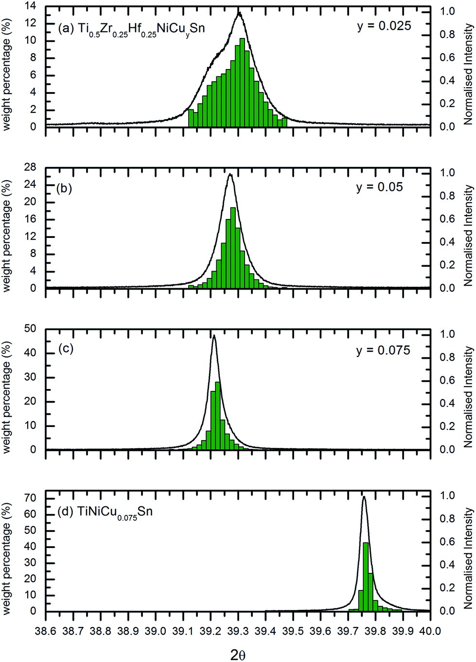
The SXRD data (Fig. S1†) shows the successful formation of HH phases, and though the y = 0.075 sample shows sharp peaks consistent with a single HH phase, the x = 0.05 and 0.025 samples show substantial peak broadening, consistent with the formation of multiple HH phases due to the poor mixing of the X-site elements.22,23Fig. 1 shows the decreasing SXRD peak width of the (4 4 2) reflection with increasing Cu content and the trend towards a single HH phase. The peak shape was fitted using multiple HH phases, with a lattice parameter difference of Δa = 0.0025 Å and fixed profile parameters so that the parent material TiNiSn is described as a single HH phase.46 The increasing homogenisation is quantified by the reduced number of phases required to describe the peak which, in turn, confirms that Cu causes a mineralising effect. Mineralising effects are commonly observed for reactions that exploit a molten flux (e.g. a NaCl–KCl eutectic)56 that partially dissolves the sample and promotes the reaction kinetics. Here, this occurs upon introduction of Cu, however, the melting point of elemental Cu (1358 K) is above the sintering temperature, suggesting that the mineralisation may instead be caused by a Cu–Sn alloy, which are observed at trace amounts in the EDS elemental mapping (Fig. 2) and which have <1123 K melting points.57 Analysis of NPD data (Fig. S2†) with its lower d-spacing resolution required only a single HH phase, enabling the experimental compositions to be verified. For these fits, the Ni and Sn sites were fixed at 100% occupancy, the Zr and Hf ratio was fixed at 1:1, while the Cu occupancy on the interstitial site and the Ti to Zr/Hf ratio on the X-site were refined freely. This confirms that the compositions of the samples are close to the nominal values, and that up to 0.075 Cu has been successfully incorporated into the vacant tetrahedral site of the structure. The occupancy of the X-sites is also confirmed to be close to the nominal split between Ti, Zr and Hf. Small amounts of HfO2 and Ni3Sn2 (<1–2 wt%) were observed for y = 0.025 and y = 0.05, but these have largely disappeared for the higher doped y = 0.075 sample (Fig. S1 and S2†), in keeping with the improved sample quality. The full results of the fits, including structural parameters and fit statistics are provided in Table S1.†
 |
| | Fig. 1 Structural evolution from synchrotron X-ray powder diffraction. Panels (a–c) show a close-up of the half-Heusler (422) reflection for selected Ti0.5Zr0.25Hf0.25NiCuySn samples. The histograms indicate the number and abundance of the HH phases needed to fit the peak shape. The HH peak width corresponds to the instrumental resolution. Panel (d) shows identical data for TiNiCu0.075Sn, which does not have X-site phase segregation, for comparison. | |
 |
| | Fig. 2 HAADF-STEM image resolving the atomic columns in a Ti0.5Zr0.25Hf0.25NiCu0.025Sn sample, viewed along a [110] direction and dominated by signals from the heaviest Sn, Zr and Hf atoms (Cu and Ni have comparatively low atomic number and are not readily observed under these acquisition conditions). The panels below are EELS maps collected by spectrum imaging and indicate the elemental distributions within the coloured region of the STEM image, with the colours of that region deriving from the (red) summed Ti, Zr and Hf signals and (green) Sn signals. EELS maps derive from the background-subtracted, deconvolved L2,3 edges of Ti, Zr, Ni and the M4,5 edges of Hf and Sn. The maps indicate occupation of the same site by Ti, Zr and Hf. Some sample drift is evident in the spectrum images. A cartoon of the [110]-oriented unit cell is also superimposed on the left of the HAADF image, with Ti/Zr/Hf atoms in green, Sn in cyan and Ni in red. | |
On atomic length-scales, occupancy of the X-site by Ti, Zr and Hf was confirmed by direct STEM imaging, as shown in Fig. 2. This figure presents a spectrum image of a section of an [110]-oriented Ti0.5Zr0.25Hf0.25NiCu0.025Sn crystal, highlighting the atomic locations of individual elements. The sample was approximately 50 nm thick and the atomic features in the main HAADF image derive from columns of several hundred atoms each, with the heaviest (Zr, Sn, Hf) elements dominating the image contrast due to the strong dependence on atomic number in this imaging mode. Despite some sample drift during acquisition, the EELS SI panels clearly locate Ti, Zr and Hf signals at the same atomic columns, suggesting mixed occupancy of the X-site. Sn signals are located on different columns, consistent with the Z-site of the HH cell whilst the Ni signal is weaker but consistent with tetrahedral site occupation. In contrast, mineralisation effects due to Cu addition are evident on micrometre length-scales, as demonstrated by the SEM data of Fig. 3. This figure presents elemental maps, derived from EDS data, collected from y = 0, 0.025 and 0.075 samples, with a separate map for each of the main elements in addition to oxygen, which can be problematic in Ti-bearing Heusler alloys58 but here is at inconsequential levels. The differences between samples are stark. Without Cu, segregation of Ti, Zr and Hf across micrometres is evident and the maps of their distributions are complementary: where one of these elements is strong, the other two are weak in signal intensity. In addition, the grain sizes are inhomogeneous, with Hf-rich grains the smallest, presumably because sintering is limited by the relatively high melting point and consequently low diffusion rates of Hf. Addition of Cu (y = 0.025 sample, middle panels of Fig. 3) reduces the elemental segregation effects to produce a more homogeneous alloy with larger grains (in agreement with the SXRD data of Fig. 1), trends that are continued in the y = 0.075 sample (lower panels of Fig. 3), where grains have increased by an order of magnitude in diameter, elemental distributions are more homogeneous and segregation within grains becomes evident. The formation of grains with a core–shell structure for y = 0.075 suggests that segregation within the y = 0.075 sample is driven by thermodynamic rather than kinetic effects (such as diffusion limitations). Previous studies have shown that Hf crystallises first from the melt to form bcc inclusions that act as nucleation seeds for grains.22 Here, the cores of larger grains are rich in both Zr and Hf and the shells are conversely rich in Ti, in accordance with the difference in elemental melting points, producing a structure similar to that seen in peritectic phase segregation from the melt.21,22 EBSD data does not indicate a substantial change in crystallography within grains, suggesting that the lattice is coherent throughout, which would account for the sharpened SXRD peaks for this composition. Higher spatial resolution analysis of phase segregation in the y = 0.025 sample is presented in Fig. S3† and shows evidence of segregation within grains; and a quantitative analysis of grain sizes for the y = 0.025 and 0.075 samples is presented in Fig. S4.† EBSD data in the latter confirm that the addition of Cu to the HH system has a mineralising effect on grain size, leading to larger grains upon annealing, with the mean size of grains more than doubling between the y = 0.025 and 0.075 samples.
 |
| | Fig. 3 SEM analysis of (a) Ti0.5Zr0.25Hf0.25NiCu0.0Sn (b) Ti0.5Zr0.25Hf0.25NiCu0.025Sn and (c) Ti0.5Zr0.25Hf0.25NiCu0.075Sn samples. Each group of panels comprises an SEM image and EDS-derived maps of elemental distribution for Ti, Zr, Hf, Ni, Cu, Sn and O, each superimposed with grain-boundary maps derived from EBSD mapping. See text for details. | |
Thermoelectric properties
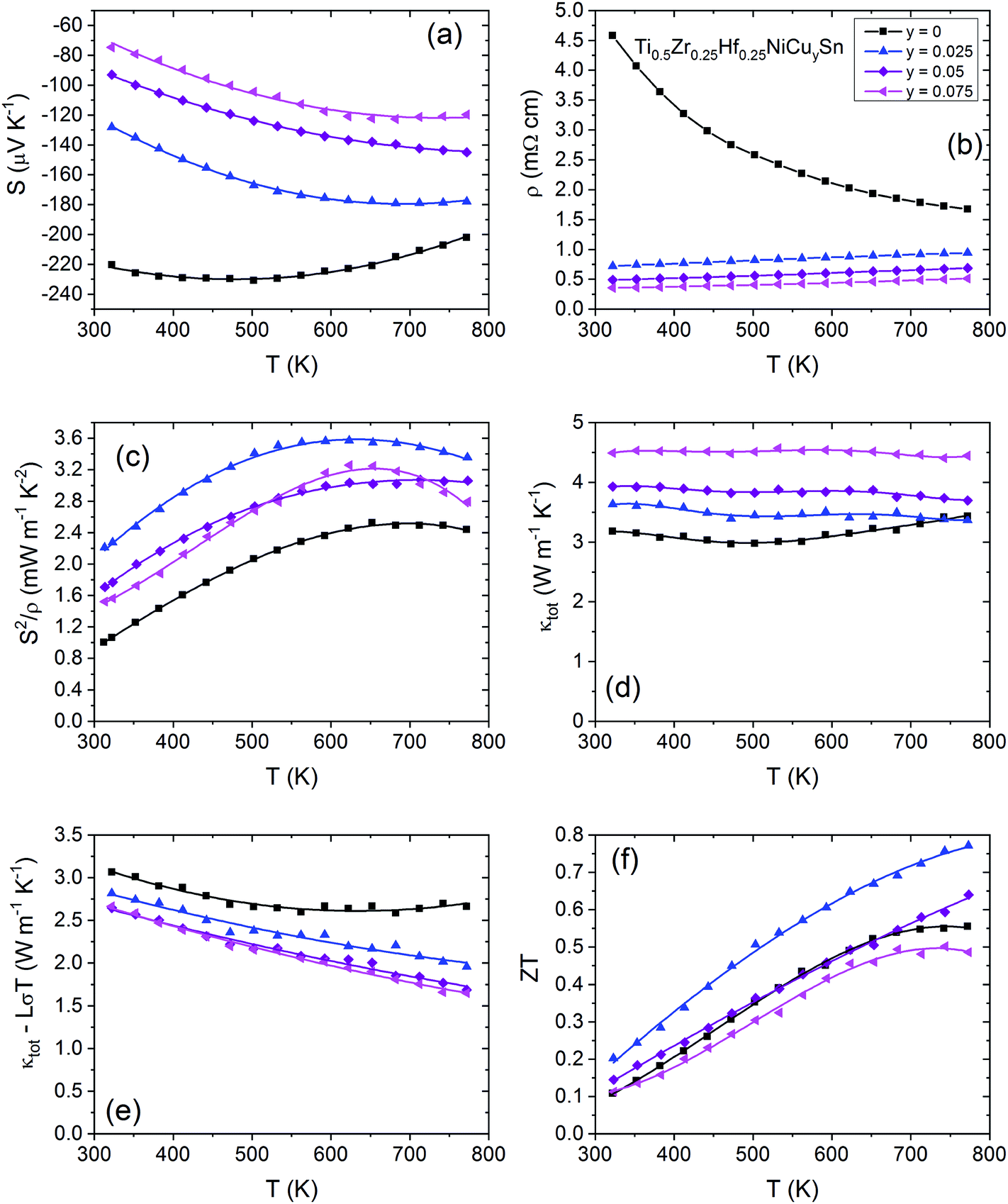
The temperature dependent electronic and thermal transport properties for the Ti0.5Zr0.25Hf0.25NiCuySn (0 ≤ y ≤ 0.075) samples are shown in Fig. 4, while the room temperature thermoelectric values are summarized in Table S2.† In all cases, the addition of Cu abruptly alters the measured parameters and thereafter there are smooth trends with increasing Cu content. This reflects the clear change in microstructure between the y = 0 and y = 0.025 samples in Fig. 3, in addition to differences in carrier concentration. The Seebeck coefficient (S) is negative for all samples, consistent with majority n-type conduction (Fig. 4a). There are large changes in both S and the electrical resistivity (ρ) with even low Cu doping, (Fig. 4b) showing that the addition of interstitial Cu electron-dopes the material and leads to a rapid transition from semiconducting to metal-like degenerate semiconductor behaviour, and simultaneously reduces ρ through mineralisation effects (discussed below). Using the ρ(T) behaviour of the semiconducting y = 0 sample, we find that the bandgap is Eg ∼ 0.1 eV, which is in good agreement with our supercell DFT calculations that show the emergence of in-gap states due to interstitial Ni, leading to a small indirect bandgap (<0.1 eV) compared to ∼0.5 eV for perfect TiNiSn. The transition from semiconducting to degenerate semiconductor behaviour leads to a large increase in the power factor (S2/ρ) for all Cu doped samples (Fig. 4c). All doped samples show an improved power factor with the y = 0.025 sample achieving S2/ρ = 3.6 mW m−1 K−2 at 623 K, a significant improvement compared to the 2.5 mW m−1 K−2 peak value for the y = 0 sample. The improvement arises because the resistivity is significantly smaller than that of the undoped sample, which is due to a combination of mineralisation and doping effects, and although |S| is diminished with respect to the undoped (y = 0) sample, it is the largest of the three doped samples.
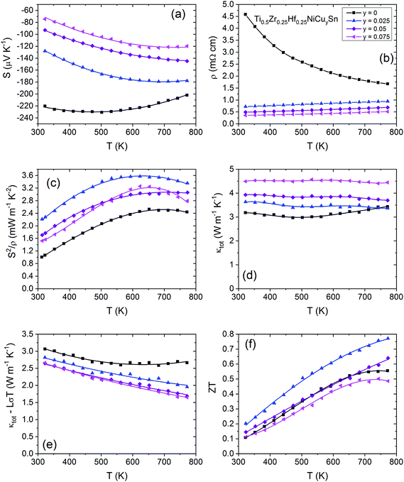 |
| | Fig. 4 Overview of the thermoelectric properties for the Ti0.5Zr0.25Hf0.25NiCuySn half-Heusler alloys. Panels (a–f) show the temperature dependence of the Seebeck coefficient (S), electrical resistivity (ρ), power factor (S2/ρ), total thermal conductivity (κ), lattice thermal conductivity (κlat) and dimensionless figure of merit (ZT). The legend is common to all panels. | |
The thermal conductivities (κ) (Fig. 4d) are largely temperature independent over the measurement range and increase by 50% with Cu content due to the increasing contribution from the electronic component (κel) (Fig. S5c†). The lattice thermal conductivities (κlat) (Fig. 4e) were extracted using the Wiedemann–Franz law using an empirical expression to estimate the Lorenz number from S(T):59 they reduce in accordance with phonon scattering by interstitial Cu. The undoped sample has a significant bipolar contribution to κ at temperatures above 600 K, which is suppressed with carrier doping resulting from the Cu interstitials.
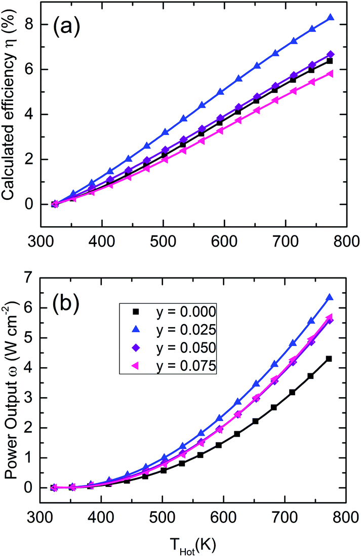
Primarily because of the semiconductor to degenerate semiconductor transition leading to a significant improvement in S2/ρ, the best dimensionless figure of merit (Fig. 4f) obtained was ZT = 0.8 at 773 K for the y = 0.025 sample. It is also important that κel is much lower than those of the more Cu-rich samples, which more than compensates for the slightly larger κlat values. The importance of this balance between S2/ρ and κel can be seen for the more degenerate samples, which show comparable ZT values to the undoped sample despite their significantly larger power factors. The improvements of S2/ρ and ZT for the y = 0.025 sample translate directly into improved predicted device properties,43 which exceed 8% efficiency at Th = 773 K and boast a power output over 6 W cm−2, around a 50% increase for both values compared to the undoped material (shown in Fig. 5). While further addition of interstitial Cu doesn't translate to better efficiency, the power outputs still show significant improvements compared to the undoped sample.
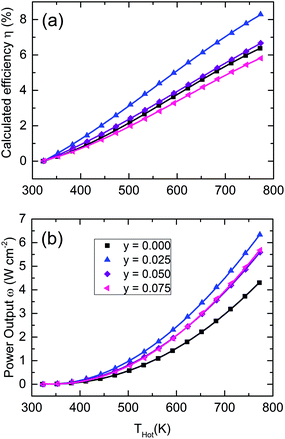 |
| | Fig. 5 (a) Calculated efficiency and (b) power output for a 2 mm long leg for the Ti0.5Zr0.25Hf0.25NiCuySn half-Heusler alloys as a function of the hot side of the device Thot when the cold side is held at Tcold = 322 K. | |
Modelling of the charge transport
Single parabolic band modelling
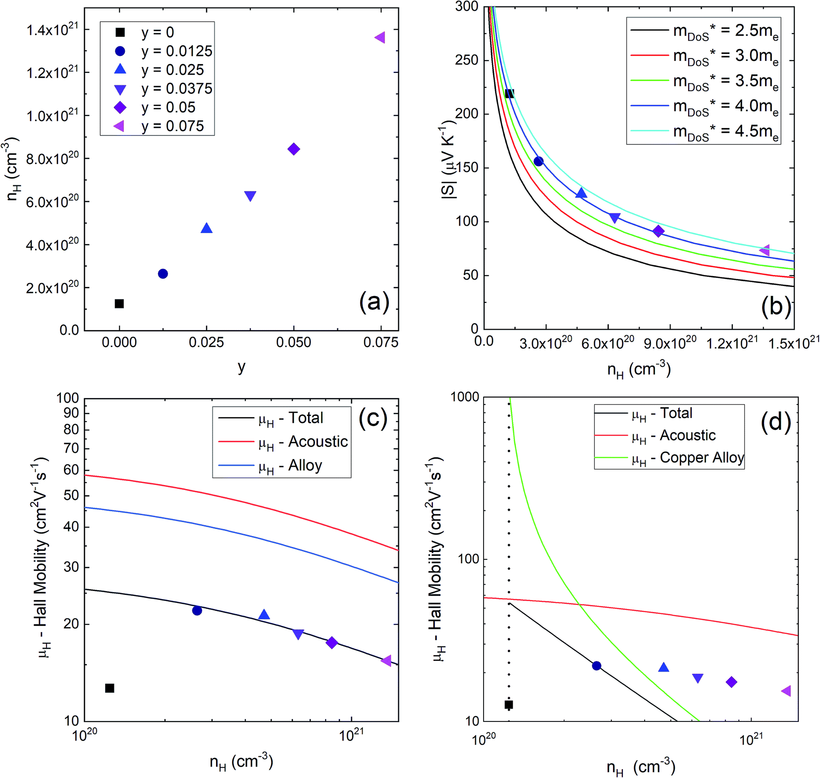
Relevant room temperature Hall mobilities and carrier concentrations can be viewed in Table S2† and all plots containing Hall data are part of Fig. 6. The addition of interstitial Cu produces a linear increase in the Hall carrier concentration (nH) (Fig. 6a) which can be attributed to the Cu 4s1 electron directly doping the conduction band, with values of the carrier concentration being comparable to the addition of 1 electron per interstitial Cu (Fig. S6†). The decrease of |S| as a function of nH (Fig. 6b) shows that all samples can be characterised by a Single Parabolic Band (SPB) with an effective mass  of 4.1me (see ESI for a description of the model used†). The unchanging effective mass values indicate that the addition of interstitial Cu does not significantly alter the conduction band structure. The DFT calculations support this rigid band picture with supercell calculations yielding a largely unchanged electronic band structure with the main effect being the n-type doping. The Hall mobility (μH) almost doubles between the y = 0 and y = 0.0125 samples, which reflects the mineralisation effects observed for even the lowest Cu doping in Fig. 3. For the doped samples μH gradually decreases as a function of nH (Fig. 6c). For further analysis, we have used the SPB model to provide theoretical fitting of the data for the doped (y > 0) samples. This follows published work,60 where two main intrinsic electron scattering mechanisms have been identified: by acoustic phonons and from alloy disorder,17 where the latter has also been linked to interstitial Ni.61 This leads to three terms in the model used here: acoustic phonon and X-site alloy scattering, which do not change with y, and scattering due to Cu interstitials, which is predicted to increase rapidly. Fitting reveals that the first two terms are enough to describe the experimental data for y > 0 (Fig. 6c), while trial fits including interstitial Cu are shown in Fig. 6d and lead to a much steeper decrease in μH. This demonstrates that μH is not affected by Cu interstitials, which is consistent with the large power factors and supported by our DFT results. We note that the gradual decrease of μH in Fig. 6c follows the expected nH dependence and does not reflect stronger coupling with phonons or alloy disorder. The strength of these interactions is characterised by the deformation and alloy scattering potentials, respectively, with fitted values Edef = 5 eV and Eal = 0.2 eV, which are comparable to published data.60 For our samples, the alloy scattering most likely originates from the X-site, as there is no evidence for the presence of substantial amounts of interstitial Ni from the NPD analysis (Table S1†). Recent literature has confirmed the suppression of the electron mobility by interstitial Ni,46,62,63 and our results on interstitial Cu are therefore highly relevant as they afford the possibility of increased phonon scattering without detriment to the electrical transport. This very different impact is supported by our DFT calculations that show the presence of in-gap states for interstitial Ni, which provide a possible route for carrier scattering, while these are absent in the Cu case.
 |
| | Fig. 6 Electronic transport in the Ti0.5Zr0.25Hf0.25NiCuySn half-Heusler alloys from Hall measurements. (a) The dependence of Hall carrier concentration (nH) on interstitial Cu content (y) is nearly linear. (b) The Pisarenko plot for these samples with the trend lines predicted using the SPB model. (c) The Hall mobilities fitted using a model considering acoustic phonon and X-site alloy electron scattering, which is found to adequately describe the experimental data for the doped samples (y > 0). (d) Trial fits that include acoustic phonon electron scattering and an alloying-type contribution due to interstitial Cu, which is not able to describe the experimental trend. | |
DFT calculations
The unfolded bandstructures from supercell calculations for Ti0.5Zr0.5NiSn, TiNi1.125Sn and TiNiCu0.125Sn are shown in Fig. 7 and are plotted together with the dispersions for ideal TiNiSn (red line), calculated in its primitive (fcc) unit cell. This enables a direct comparison between parent and substituted compositions. The bandstructure of Ti0.5Zr0.5NiSn (Fig. 7a) shows no significant change to the electronic structure of the parent TiNiSn, with similar bandgap and only modest changes to the conduction band dispersions. Some additional electronic states appear at the X and W points, but these are well separated from the Fermi energy. The relatively small changes are in-keeping with the established similarity between the bandstructures of the XNiSn parent materials.64,65 By contrast, the calculations with interstitial Ni and Cu show the emergence of a new partially filled band at the conduction band minimum (X point; Fig. 7b and c). The curvature of this band is sharper, suggesting a lower carrier effective mass  compared to TiNiSn. This change is not picked up in the Hall data for our samples, which have an unchanged
  (here Nv = 3 is the valley degeneracy) but this may simply reflect the presence of small amounts of interstitial Ni in the y = 0 sample. In addition, the Fermi energy is up-shifted by the additional electron from Cu, which means there is a greater filling of the conduction band electron pocket. This agrees with the increase in nH at the rate of 1 electron per interstitial Cu from the Hall measurements. The final and perhaps most significant observation is the absence of localised electronic defect states in the bandgap along the X – Γ – L direction for interstitial Cu (Fig. 7c), whereas these do occur for interstitial Ni (Fig. 7b). As discussed in the previous section, the absence of these in-gap defect states, which provide a route for carrier scattering, is consistent with the unchanged electron mobility for Cu interstitials.
 |
| | Fig. 7 Unfolded band structures of 2 × 2 × 2 supercells for (a) Ti0.5Zr0.5NiSn, (b) TiNi1.125Sn and (c) TiNiCu0.125Sn. The value of 1 on the colour bar corresponds to a single non-degenerate band per energy interval. The continuous red line is the band structure for TiNiSn, calculated using a primitive fcc unit cell. The dotted red line indicates the Fermi energy. | |
Modelling of the thermal transport
Callaway modelling
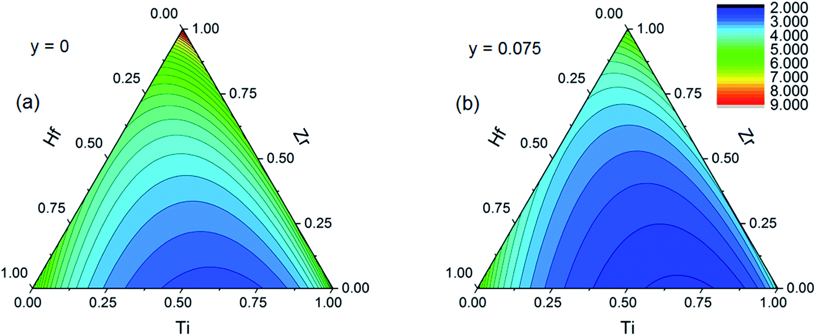
Accurate modelling of the thermal conductivity of such a complicated materials system, containing point defects in the form of alloying and interstitials, as well as microstructural inhomogeneity is both challenging and often overlooked. Theoretical work66 on defect-free HH alloys has suggested that the bulk of heat carrying phonons have mean free paths less than 1 μm. Our microscopy has not revealed any nanostructures at significant number densities, leaving point defects as the most likely source of thermal conductivity reduction. The average grain size for y = 0 is ∼2 μm, which is already too large to expect a significant reduction due to boundary scattering.18,19 For y > 0, the average grain size increases, while the improved homogenisation of Ti, Zr and Hf will maximise the point-defect disorder. We have previously described the impact of interstitials in TiNiSn and find that they embed a large disorder phonon scattering effect, comparable to the introduction of vacancies, and much stronger than conventional alloying.43,46 Here, we extend the Callaway approach and focus on the impact of alloying at fixed levels of Cu interstitials. This approach uses XNiCuySn end-members to define the thermal conductivity of a ‘perfect’ crystal (κPlat) in the absence of point-defect phonon scattering (Table S3†). The expected phonon scattering due to mass (ΓM) and size (ΓS) disorder is then calculated and used to predict a value for κlat (ref. 67) and this can be compared to the measured values. The predicted κlat is relatively insensitive to the imperfect mixing of the X elements and a statistical distribution was assumed. Table 1 summarises the results of these calculations for y = 0 and y = 0.075 and the conclusion is that the model predicts the measured κlat within the uncertainty of the experimental values. This confirms that the impact of alloying is the conventional phonon point-defect scattering due to mass and size differences. The good agreement allows κlat to be predicted for any combination of alloying elements, guiding further exploration. Pseudo ternary TiaZrbHfcNiCuySn (y = 0 and 0.075) phase diagrams illustrating the variations in κlat due to mass and size disorder are shown in Fig. 8. The two plots have a similar form and the effect of Cu doping is to depress κlat for all compositions. The lowest value of κlat is for compositions around Ti0.7Hf0.3NiCu0.075Sn, which provides the best balance of mass disorder, the κlat values of the parent phases and beneficial scattering from interstitial Cu. To best manage the electronic properties, in particular κel, one would need to reduce the amount of interstitial Cu to 0.01 < y < 0.025.
Table 1 Calculated mass (ΓM) and strain disorder (ΓS) parameters for the X-site, Callaway-model predicted and measured lattice thermal conductivities (κlat) for the Ti0.5Zr0.25Hf0.25NiCuySn samples with no and 7.5% interstitial Cu
|
y
|
Γ
M,X-site
|
Γ
S,X-site
|
Predicted κlat (W m−1 K−1) |
Experimental κlat (W m−1 K−1) |
| 0 |
0.1575 |
0.0154 |
3.10 |
3.07 (±0.31) |
| 0.075 |
0.1520 |
0.0149 |
2.50 |
2.66 (±0.27) |
 |
| | Fig. 8 Predicted lattice thermal conductivity in the ternary TiaZrbHfcNiCuySn half-Heusler phase diagram for two levels of interstitial Cu (y = 0 and y = 0.075). The intensity scale is in W m−1 K−1. The lowest κlat = 2.8 W m−1 K−1 (y = 0) and κlat = 2.2 W m−1 K−1 (y = 0.075) occur on the Ti-Hf axis for ∼30% Hf. | |
Conclusions
The incorporation of Cu into XNiSn HH alloys is a promising route to enhance their thermoelectric performance. Its presence during synthesis promotes homogenisation of Ti, Zr and Hf, and leads to improved grain growth, enabling a doubling of the electron mobility. This mineralising effect likely occurs via small amounts of molten Cu–Sn alloy, which locally dissolves reagents and increases diffusion rates. In the formed products, Cu occupies the interstitial site at close to the nominal values. Despite the complexity of the microstructure, the trends in the thermoelectric properties of the doped samples can be largely understood by point-defect electron and phonon scattering mechanisms. Cu is an effective n-type dopant with a dual function as an effective phonon scatterer without detrimental impact on the electron mobility (in contrast to interstitial Ni), leading to enhanced ZT values. The X-site alloying causes conventional mass and size disorder phonon scattering, leading to substantial reductions in thermal conductivity, with minor reductions of the electron mobility as characterised by the low value of the alloy scattering potential in the SPB model.
Maximum achievable performance
The SPB analysis predicts that tuning the carrier concentration to ∼2 × 1020 cm−3 (y ∼ 0.01; Fig. S7d†), will enable a 10–15% improvement, yielding ZT ∼ 0.9 at 773 K. Furthermore, despite our ability to model the thermoelectric trends, there could be hidden effects that are invariant across the samples. For example, comparable Sb doped samples prepared via melt-based routes routinely achieve S2/ρ = 5–6 W m−1 K−2.15,22 If similar values could be achieved in samples with interstitial Cu – and there is no reason why this should not be possible since interstitial Cu and X-site alloying do strongly affect the electron mobility – then ZT could readily be improved to above unity, and in the best-case scenario ZT ∼ 1.3 at 773 K is possible. Cu interstitials could potentially also find application in other half-Heusler systems as n-type dopants and phonon scattering centres. Investigation of the solubility of interstitial Cu in other half-Heuslers, including some of the best current p-types to develop n-types based on near identical chemical compositions, is of considerable interest.
Author contributions
S. A. B. synthesised the materials, undertook thermoelectric property measurements, and analysed all diffraction data; R. J. Q. undertook the SPB and Callaway modelling, J. E. H. and D. A. M. collected and analysed all microscopy data; K. D. undertook the DFT calculations; R. I. S. and A. R. B. provided assistance with data collection at the ISIS Muon and Neutron Source and Diamond Light Source, respectively; E. D. and I. F. collected the Hall data; K. R. supervised the DFT calculations; J.-W. G. B. conceived the project, supervised sample preparation, thermoelectric characterisation, analysis of diffraction data and SPB modelling. J.-W. G. B. and D. A. M. wrote the manuscript with assistance from S. A. B, R. J. Q and K. R.
Conflicts of interest
There are no conflicts of interest to declare.
Acknowledgements
J.-W. G. B. acknowledges EPSRC grant EP/N01717X/1; D. A. M. acknowledges EPSRC grants EP/N017218/1 and EP/P001483/1; and K. R. acknowledges grant EP/N01703X/1. The STFC is acknowledged for beam time at the Diamond Light Source (award EE14032) and ISIS neutron and muon facility (award RB1610148). DFT calculations were performed using STFC Scientific Computing Department's “SCARF” cluster. Raw data underpinning this work is available at DOI: http://10.5525/gla.researchdata.912.
References
-
CRC Handbook of Thermoelectrics, ed. D. M. Rowe, CPC Press, Boca Raton, 1995 Search PubMed.
-
Thermoelectrics and its Energy Harvesting, ed. D. M. Rowe, CRC Press, Boca Raton, 2012 Search PubMed.
- J. W. G. Bos and R. A. Downie, J. Phys.: Condens. Matter, 2014, 26, 433201 CrossRef.
- J. J. Yu, K. Y. Xia, X. B. Zhao and T. J. Zhu, J. Phys. D: Appl. Phys., 2018, 51, 113001 CrossRef.
- T. J. Zhu, C. G. Fu, H. H. Xie, Y. T. Liu and X. B. Zhao, Adv. Energy Mater., 2015, 5, 1500588 CrossRef.
- L. H. Huang, Q. Y. Zhang, B. Yuan, X. Lai, X. Yan and Z. F. Ren, Mater. Res. Bull., 2016, 76, 107–112 CrossRef CAS.
- C. G. Fu, S. Q. Bai, Y. T. Liu, Y. S. Tang, L. D. Chen, X. B. Zhao and T. J. Zhu, Nat. Commun., 2015, 6, 8144 CrossRef PubMed.
- C. G. Fu, T. J. Zhu, Y. T. Liu, H. H. Xie and X. B. Zhao, Energy Environ. Sci., 2015, 8, 216–220 RSC.
- R. Hea, D. Kraemer, J. Mao, L. Zeng, Q. Jie, Y. C. Lan, C. H. Li, J. Shuai, H. S. Kim, Y. Liu, D. Broido, C. W. Chu, G. Chen and Z. Ren, Proc. Natl. Acad. Sci. U. S. A., 2016, 113, 13576–13581 CrossRef.
- H. T. Zhu, R. He, J. Mao, Q. Zhu, C. H. Li, J. F. Sun, W. Y. Ren, Y. M. Wang, Z. H. Liu, Z. J. Tang, A. Sotnikov, Z. M. Wang, D. Broido, D. J. Singh, G. Chen, K. Nielsch and Z. F. Ren, Nat. Commun., 2018, 9, 2497 CrossRef PubMed.
- J. J. Yu, C. G. Fu, Y. T. Liu, K. Y. Xia, U. Aydemir, T. C. Chasapis, G. J. Snyder, X. B. Zhao and T. J. Zhu, Adv. Energy Mater., 2018, 8, 1701313 CrossRef.
- H. T. Zhu, J. Mao, Y. W. Li, J. F. Sun, Y. M. Wang, Q. Zhu, G. N. Li, Q. C. Song, J. W. Zhou, Y. H. Fu, R. He, T. Tong, Z. H. Liu, W. Y. Ren, L. You, Z. M. Wang, J. Luo, A. Sotnikov, J. M. Bao, K. Nielsch, G. Chen, D. J. Singh and Z. F. Ren, Nat. Commun., 2019, 10, 270 CrossRef PubMed.
- C. Yu, T. J. Zhu, R. Z. Shi, Y. Zhang, X. B. Zhao and J. He, Acta Mater., 2009, 57, 2757–2764 CrossRef CAS.
- L. Chen, S. Gao, X. Zeng, A. M. Dehkordi, T. M. Tritt and S. J. Poon, Appl. Phys. Lett., 2015, 107, 041902 CrossRef.
- M. Gurth, G. Rogl, V. V. Romaka, A. Grytsiv, E. Bauer and P. Rogl, Acta Mater., 2016, 104, 210–222 CrossRef.
- S. Sakurada and N. Shutoh, Appl. Phys. Lett., 2005, 86, 082105 CrossRef.
- Y. T. Liu, C. G. Fu, K. Y. Xia, J. J. Yu, X. B. Zhao, H. G. Pan, C. Felser and T. J. Zhu, Adv. Mater., 2018, 30, 1800881 CrossRef.
- S. Bhattacharya, M. J. Skove, M. Russell, T. M. Tritt, Y. Xia, V. Ponnambalam, S. J. Poon and N. Thadhani, Phys. Rev. B: Condens. Matter Mater. Phys., 2008, 77, 184203 CrossRef.
- G. Joshi, X. Yan, H. Z. Wang, W. S. Liu, G. Chen and Z. F. Ren, Adv. Energy Mater., 2011, 1, 643–647 CrossRef CAS.
- X. A. Yan, G. Joshi, W. S. Liu, Y. C. Lan, H. Wang, S. Lee, J. W. Simonson, S. J. Poon, T. M. Tritt, G. Chen and Z. F. Ren, Nano Lett., 2011, 11, 556–560 CrossRef CAS PubMed.
- S. Populoh, M. H. Aguirre, O. C. Brunko, K. Galazka, Y. Lu and A. Weidenkaff, Scr. Mater., 2012, 66, 1073–1076 CrossRef CAS.
- M. Schwall and B. Balke, Phys. Chem. Chem. Phys., 2013, 15, 1868–1872 RSC.
- R. A. Downie, D. A. MacLaren and J. W. G. Bos, J. Mater. Chem. A, 2014, 2, 6107–6114 RSC.
- K. Kirievsky, Y. Gelbstein and D. Fuks, J. Solid State Chem., 2013, 203, 247–254 CrossRef CAS.
- A. Page, C. Uher, P. F. Poudeu and A. Van der Ven, Phys. Rev. B: Condens. Matter Mater. Phys., 2015, 92, 174102 CrossRef.
- D. T. Do, S. D. Mahanti and J. J. Pulikkoti, J. Phys.: Condens. Matter, 2014, 26, 275501 CrossRef PubMed.
- M. Gurth, A. Grytsiv, J. Vrestal, V. V. Romaka, G. Giester, E. Bauer and P. Rogl, RSC Adv., 2015, 5, 92270–92291 RSC.
- J. P. A. Makongo, D. K. Misra, X. Y. Zhou, A. Pant, M. R. Shabetai, X. L. Su, C. Uher, K. L. Stokes and P. F. P. Poudeu, J. Am. Chem. Soc., 2011, 133, 18843–18852 CrossRef CAS.
- J. E. Douglas, C. S. Birkel, M. S. Miao, C. J. Torbet, G. D. Stucky, T. M. Pollock and R. Seshadri, Appl. Phys. Lett., 2012, 101, 183902 CrossRef.
- Y. W. Chai and Y. Kimura, Appl. Phys. Lett., 2012, 100, 033114 CrossRef.
- Y. F. Liu, P. Sahoo, J. P. A. Makongo, X. Y. Zhou, S. J. Kim, H. Chi, C. Uher, X. Q. Pan and P. F. P. Poudeu, J. Am. Chem. Soc., 2013, 135, 7486–7495 CrossRef CAS PubMed.
- C. S. Birkel, J. E. Douglas, B. R. Lettiere, G. Seward, N. Verma, Y. C. Zhang, T. M. Pollock, R. Seshadri and G. D. Stucky, Phys. Chem. Chem. Phys., 2013, 15, 6990–6997 RSC.
- Y. W. Chai and Y. Kimura, Acta Mater., 2013, 61, 6684–6697 CrossRef CAS.
- J. E. Douglas, C. S. Birkel, N. Verma, V. M. Miller, M. S. Miao, G. D. Stucky, T. M. Pollock and R. Seshadri, J. Appl. Phys., 2014, 115, 043720 CrossRef.
- J. E. Douglas, P. A. Chater, C. M. Brown, T. M. Pollock and R. Seshadri, J. Appl. Phys., 2014, 116, 163514 CrossRef.
- Y. Kimura and Y. W. Chai, JOM, 2015, 67, 233–245 CrossRef CAS.
- P. Sauerschnig, A. Grytsiv, J. Vrestal, V. V. Romaka, B. Smetana, G. Giester, E. Bauer and P. Rogl, J. Alloys Compd., 2018, 742, 1058–1082 CrossRef CAS.
- M. N. Guzik, M. Schrade, R. Tofan, P. A. Carvalho, K. Berland, M. H. Sorby, C. Persson, A. E. Gunnaes and B. C. Hauback, CrystEngComm, 2019, 21, 3330–3342 RSC.
- K. S. Kim, Y. M. Kim, H. Mun, J. Kim, J. Park, A. Y. Borisevich, K. H. Lee and S. W. Kim, Adv. Mater., 2017, 29, 1702091 CrossRef.
- H. J. Lee, K. H. Lee, L. Fu, G. Han, H.-S. Kim, S.-I. Kim, Y.-M. Kim and S. W. Kim, Acta Mater., 2019, 180, 97–104 CrossRef CAS.
- R. A. Downie, R. I. Smith, D. A. MacLaren and J. W. G. Bos, Chem. Mater., 2015, 27, 2449–2459 CrossRef CAS.
- R. A. Downie, S. A. Barczak, R. I. Smith and J. W. G. Bos, J. Mater. Chem. C, 2015, 3, 10534–10542 RSC.
- S. A. Barczak, J. E. Halpin, J. Buckman, R. Decourt, M. Pollet, R. I. Smith, D. A. MacLaren and J. W. G. Bos, ACS Appl. Mater. Interfaces, 2018, 10, 4786–4793 CrossRef CAS PubMed.
- R. A. Downie, D. A. MacLaren, R. I. Smith and J. W. G. Bos, Chem. Commun., 2013, 49, 4184–4186 RSC.
-
S. A. Barczak, PhD thesis, Heriot-Watt University, 2018.
- S. A. Barczak, J. Buckman, R. I. Smith, A. R. Baker, E. Don, I. Forbes and J. W. G. Bos, Materials, 2018, 11, 536 CrossRef PubMed.
-
A. C. Larson and R. B. Von Dreele, General Structure Analysis System (GSAS), Los Alamos National Laboratory Report LAUR 86-748, 2000 Search PubMed.
- B. H. Toby, J. Appl. Crystallogr., 2001, 34, 210–213 CrossRef CAS.
- A. A. Coelho, J. S. O. Evans, I. R. Evans, A. Kern and S. Parsons, Powder Diffr., 2011, 26, S22–S25 CrossRef CAS.
-
B. Beausir and J.-J. Fundenberger, ATOM – Analysis Tools for Orientation Maps, 2018, http://atom-software.eu Search PubMed.
- C. Jeanguillaume and C. Colliex, Ultramicroscopy, 1989, 28, 252–257 CrossRef.
- S. J. Clark, M. D. Segall, C. J. Pickard, P. J. Hasnip, M. J. Probert, K. Refson and M. C. Payne, Z. Kristallogr. Cryst. Mater., 2005, 220, 567–570 CAS.
- J. P. Perdew, K. Burke and M. Ernzerhof, Phys. Rev. Lett., 1996, 77, 3865–3868 CrossRef CAS.
- P. Brommer and D. Quigley, J. Phys.: Condens. Matter, 2014, 26, 485501 CrossRef.
- V. Popescu and A. Zunger, Phys. Rev. B: Condens. Matter Mater. Phys., 2012, 85, 485501 Search PubMed.
- S. Ishiwata, J. W. G. Bos, Q. Huang and R. J. Cava, J. Phys.: Condens. Matter, 2006, 18, 3745–3752 CrossRef CAS.
- N. Saunders and A. P. Miodownik, Bull. Alloy Phase Diagrams, 1990, 11, 278–287 CrossRef CAS.
- R. W. H. Webster, J. E. Halpin, S. R. Popuri, J. W. G. Bos and D. A. MacLaren, APL Mater., 2019, 7, 013206 CrossRef.
- H. S. Kim, Z. M. Gibbs, Y. L. Tang, H. Wang and G. J. Snyder, APL Mater., 2015, 3, 041506 CrossRef.
- H. H. Xie, H. Wang, Y. Z. Pei, C. G. Fu, X. H. Liu, G. J. Snyder, X. B. Zhao and T. J. Zhu, Adv. Funct. Mater., 2013, 23, 5123–5130 CrossRef CAS.
- H. H. Xie, H. Wang, C. G. Fu, Y. T. Liu, G. J. Snyder, X. B. Zhao and T. J. Zhu, Sci. Rep., 2014, 4, 6888 CrossRef CAS PubMed.
- W. Y. Ren, H. T. Zhu, J. Mao, L. You, S. W. Song, T. Tong, J. M. Bao, J. Luo, Z. M. Wang and Z. F. Ren, Adv. Electron. Mater., 2019, 5, 1900166 CrossRef.
- Y. L. Tang, X. S. Li, L. H. J. Martin, E. C. Reyes, T. Ivas, C. Leinenbach, S. Anand, M. Peters, G. J. Snyder and C. Battaglia, Energy Environ. Sci., 2018, 11, 311–320 RSC.
- S. Ogut and K. M. Rabe, Phys. Rev. B: Condens. Matter Mater. Phys., 1995, 51, 10443–10453 CrossRef CAS.
- M. Zahedifar and P. Kratzer, Phys. Rev. B, 2018, 97, 035204 CrossRef CAS.
- J. Shiomi, K. Esfarjani and G. Chen, Phys. Rev. B: Condens. Matter Mater. Phys., 2011, 84, 104302 CrossRef.
- J. Yang, G. P. Meisner and L. Chen, Appl. Phys. Lett., 2004, 85, 1140–1142 CrossRef CAS.
Footnote |
| † Electronic supplementary information (ESI) available: Tables with detailed structural information, details of the SPB analysis, Rietveld fits to SXRD and NPD data and additional electron microscopy images. See DOI: 10.1039/c9ta10128d |
|
| This journal is © The Royal Society of Chemistry 2019 |
Click here to see how this site uses Cookies. View our privacy policy here. 
 Open Access Article
 This Open Access Article is licensed under a
  a,
J. E.
Halpin
a,
J. E.
Halpin


 of 4.1me (see ESI for a description of the model used†). The unchanging effective mass values indicate that the addition of interstitial Cu does not significantly alter the conduction band structure. The DFT calculations support this rigid band picture with supercell calculations yielding a largely unchanged electronic band structure with the main effect being the n-type doping. The Hall mobility (μH) almost doubles between the y = 0 and y = 0.0125 samples, which reflects the mineralisation effects observed for even the lowest Cu doping in Fig. 3. For the doped samples μH gradually decreases as a function of nH (Fig. 6c). For further analysis, we have used the SPB model to provide theoretical fitting of the data for the doped (y > 0) samples. This follows published work,60 where two main intrinsic electron scattering mechanisms have been identified: by acoustic phonons and from alloy disorder,17 where the latter has also been linked to interstitial Ni.61 This leads to three terms in the model used here: acoustic phonon and X-site alloy scattering, which do not change with y, and scattering due to Cu interstitials, which is predicted to increase rapidly. Fitting reveals that the first two terms are enough to describe the experimental data for y > 0 (Fig. 6c), while trial fits including interstitial Cu are shown in Fig. 6d and lead to a much steeper decrease in μH. This demonstrates that μH is not affected by Cu interstitials, which is consistent with the large power factors and supported by our DFT results. We note that the gradual decrease of μH in Fig. 6c follows the expected nH dependence and does not reflect stronger coupling with phonons or alloy disorder. The strength of these interactions is characterised by the deformation and alloy scattering potentials, respectively, with fitted values Edef = 5 eV and Eal = 0.2 eV, which are comparable to published data.60 For our samples, the alloy scattering most likely originates from the X-site, as there is no evidence for the presence of substantial amounts of interstitial Ni from the NPD analysis (Table S1†). Recent literature has confirmed the suppression of the electron mobility by interstitial Ni,46,62,63 and our results on interstitial Cu are therefore highly relevant as they afford the possibility of increased phonon scattering without detriment to the electrical transport. This very different impact is supported by our DFT calculations that show the presence of in-gap states for interstitial Ni, which provide a possible route for carrier scattering, while these are absent in the Cu case.
 compared to TiNiSn. This change is not picked up in the Hall data for our samples, which have an unchanged
  (here Nv = 3 is the valley degeneracy) but this may simply reflect the presence of small amounts of interstitial Ni in the y = 0 sample. In addition, the Fermi energy is up-shifted by the additional electron from Cu, which means there is a greater filling of the conduction band electron pocket. This agrees with the increase in nH at the rate of 1 electron per interstitial Cu from the Hall measurements. The final and perhaps most significant observation is the absence of localised electronic defect states in the bandgap along the X – Γ – L direction for interstitial Cu (Fig. 7c), whereas these do occur for interstitial Ni (Fig. 7b). As discussed in the previous section, the absence of these in-gap defect states, which provide a route for carrier scattering, is consistent with the unchanged electron mobility for Cu interstitials.