
 Open Access Article
 This Open Access Article is licensed under a
 Creative Commons Attribution 3.0 Unported Licence
A solution-based ALD route towards (CH3NH3)(PbI3) perovskite via lead sulfide films†
Vanessa M.
Koch
a,
Maïssa K. S.
Barr
 a,
Pascal
Büttner
a,
Ignacio
Mínguez-Bacho
a,
Dirk
Döhler
a,
Bettina
Winzer
b,
Elisabeth
Reinhardt
bc,
Doris
Segets
d and
Julien
Bachmann
*ae
a,
Pascal
Büttner
a,
Ignacio
Mínguez-Bacho
a,
Dirk
Döhler
a,
Bettina
Winzer
b,
Elisabeth
Reinhardt
bc,
Doris
Segets
d and
Julien
Bachmann
*ae
aDepartment of Chemistry and Pharmacy, Chemistry of Thin Film Materials, Friedrich-Alexander-Universität Erlangen-Nürnberg, IZNF Cauerstr. 3, 91058 Erlangen, Germany. E-mail: julien.bachmann@fau.de
bInstitute of Particle Technology (LFG), Friedrich-Alexander-Universität Erlangen-Nürnberg, Cauerstraße 4, 91058 Erlangen, Germany
cInterdisciplinary Center for Functional Particle Systems (FPS), Friedrich-Alexander-Universität Erlangen-Nürnberg, Haberstraße 9a, 91058 Erlangen, Germany
dProcess Technology for Electrochemical Functional Materials, Institute for Combustion and Gas Dynamics – Reactive Fluids (IVG-RF), Center for Nanointegration Duisburg-Essen (CENIDE), University of Duisburg-Essen (UDE), Carl-Benz-Straße 199, 47057 Duisburg, Germany
eInstitute of Chemistry, Saint Petersburg State University, Universitetskii pr. 26, Saint Petersburg 198504, Russian Federation
First published on 23rd October 2019
Abstract
We present a procedure to grow thin films of lead sulfide (PbS) with ‘solution Atomic Layer Deposition’ (sALD), a technique which transfers the principles of ALD from the gas phase (gALD) to liquid processing. PbS thin films are successfully deposited on planar and porous substrates with a procedure that exhibits the unique ALD characteristics of self-limiting surface chemistry and linear growth at room temperature. The polycrystalline p-type PbS films are stoichiometric and pure. They are converted to the hybrid perovskite methylammonium iodoplumbate (methylammonium lead iodide, MAPI, CH3NH3PbI3) by annealing to 150 °C in the presence of vapors from methylammonium iodide (MAI).
Introduction
Hybrid perovskites have established themselves as a family of solution-processable absorber materials for photovoltaic devices able to reach efficiencies comparable to those of traditional cells (record efficiency to date 23.7% for a single junction,1 28% in a tandem configuration with an additional silicon-based junction).2 The most prominent members of this family are the plumbates, exemplified by methylammonium iodoplumbate (CH3NH3PbI3), also called MAPI. Established methods to deposit perovskites such as blade coating, spin-coating and dip-coating,3,4 are facile to implement and fast to execute but limited in terms of scalability and thickness control on non-planar substrates. Imperfect reproducibility and homogeneity result in a spread of performance in the resulting photovoltaic devices.Atomic layer deposition (ALD) is a thin film coating technique that provides precisely these advantages of homogeneity over large areas, absolute reproducibility and outstanding thickness control in non-planar cases. Moreover, the technique is scalable and can achieve throughputs on the order of 100 m2 per hour as demonstrated already.5,6 The method bases on the repetition of two (or more) well-defined surface reactions between molecular precursors and the solid surface that are self-terminating and complementary. It therefore yields conformal coatings, even in highly porous substrates, with atomic-scale control. Traditionally, ALD is performed from the gas phase (gALD), which limits the choice of precursors to volatile ones, that is, small, neutral molecules. A solution-based variant of the technique, ‘solution ALD’ or sALD, has recently been demonstrated to transfer the advantages of traditional gas-phase ALD to solution processing,7,8 but has not been applied to the formation of ternary compounds such as perovskites so far.
Here, we establish a route for generating films of MAPI based on sALD, that is, a fully scalable solution processing method with outstanding control even in porous systems. The crucial step is an sALD reaction developed for lead sulfide (PbS) from the constituting salts (which could not be exploited as precursors in gALD), followed by a complete vapor annealing conversion of PbS to MAPI. Lead iodide (PbI2) is the standard starting material for the conversion to MAPI, for which various approaches have been investigated.9–11 A two-step conversion has recently been demonstrated from PbS, namely via PbI2.12 A direct conversion from PbS to MAPI has not been reported yet.
We note that PbS is also an interesting semiconductor itself with a variety of applications. Thin films of it have been used in infrared detectors for decades.13 Moreover, photovoltaic cells with PbS quantum dots (QDs) on wide bandgap semiconductors such as titanium dioxide (TiO2) have been developed.14 Established methods of depositing PbS cover liquid-phase techniques such as electrodeposition (ED), chemical bath deposition (CBD) or successive ionic layer adsorption and reaction (SILAR).15–18 PbS is also accessible via traditional gas-phase ALD based on highly toxic, not inexpensive, volatile molecular lead precursors.19–21
The current paper establishes a simple, low-cost sALD method to PbS films with reduced health hazard. The data evidence the high purity and crystallinity of the deposit obtained at room temperature via solution processing. A conversion of PbS to MAPI via vapor annealing in one step yields a pure, functional semiconductor material. This approach could significantly broaden the field of low-cost printed devices.
Results and discussion
Solution ALD of PbS
The poorly soluble solid PbS can be formed via direct mixing of soluble lead(II) and sulfide salts (CBD).16,22 A more controlled variant has been demonstrated in the SILAR procedure.17,18 SILAR can be considered as a form of ALD in which oppositely charged ions serve as precursors and chemisorb to the surface in a manner limited by electrostatics (in addition to the solid formation energy). At each reaction step, the chemisorption of ions generating the solid (lead(II) and sulfide in our particular case) can only proceed until a monolayer has bonded and generated an electrostatically charged surface (Scheme 1). We have generalized the SILAR principles in a dedicated ‘solution ALD’ (sALD) setup that flows methanolic solutions of lead(II) nitrate and sodium sulfide in alternating manner over the substrate, in distinct steps separated by pure solvent purges. Our sALD system is capable of performing large numbers of cycles, upon which brown PbS films grow (Fig. S1†) in the self-limiting manner that characterizes ALD.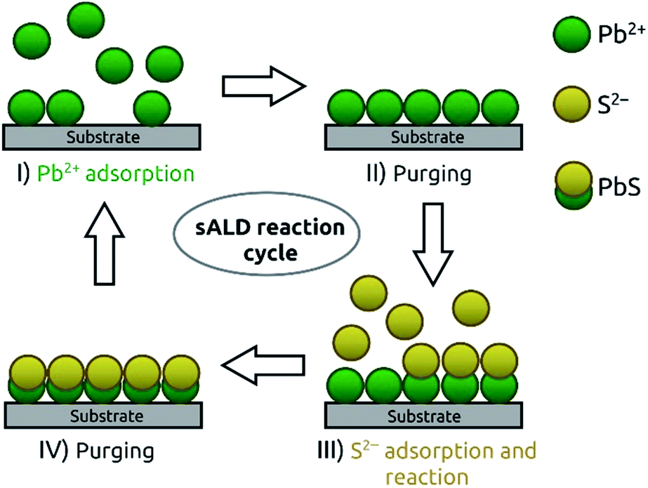 | ||
| Scheme 1 PbS formation in sALD. | ||
Let us start with TiO2 as our standard substrate (gALD-coated on Si/SiO2 wafer pieces) due to its common use in photovoltaic devices.23 The demonstration of the ‘self-limiting’ ALD character is provided by the experimentally observed saturation of growth rate of PbS in dependence of varying precursor dosage and purge durations (Table 1 and Fig. 1). Each growth rate shown in Fig. 1 is derived from three distinct thickness measurements of the deposited PbS films performed by spectroscopic ellipsometry after three distinct numbers of cycles.
| Pulse duration/s | Purge duration/s | c[Pb(NO3)2, Na2S·9H2O]/mM | |
|---|---|---|---|
| Standard | 15 | 40 | 1 |
| Pulse variation | 1, 5, 10, 15, 20, 25 | 90 | 1 |
| Purge variation | 15 | 5, 10, 15, 20, 30, 40, 50, 90 | 1 |
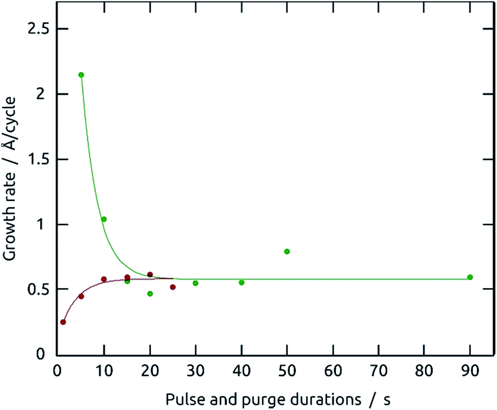 | ||
| Fig. 1 Experimental saturation behavior of the growth as a function of the precursor pulse and purge durations (red and green, respectively) of the sALD reaction between Pb(NO3)2 and Na2S·9H2O on TiO2-coated Si/SiO2 wafer. Each growth rate results from three thickness measurements by spectroscopic ellipsometry. | ||
When the precursor dosage is varied by changing the precursor pulse durations of Pb(NO3)2 and Na2S·9H2O (both 1 mM) from 1 s to 25 s in steps of 5 s, while the purge durations are maintained constant at 90 s, a constant growth rate is reached from a minimum pulse duration of 10 s (red datapoints). Below this value, no full coverage of the surface can be ensured. A complementary saturation experiment is provided by varying the purge duration for both precursors from 5 s to 90 s in steps of 5 s, whereas the pulse duration for both precursors is kept constant (at 15 s). It indicates that uncontrolled, direct contact between precursors is avoided for purges of at least 15 s (green datapoints). These curves confirm that the reaction of the precursors with the surface is self-limiting, as it should in ALD growth. They also suggest 15 s and 40 s as the standard values for pulse and purge durations, respectively.
A more complete picture of the film growth upon repeated cycling is provided (using the standard parameters) in Fig. 2 for two substrates with contrasting surface chemistries, namely wafers gALD-coated with TiO2 and with ZnS (green and red datapoints, respectively). Here, spectroscopic ellipsometry (dots) is complemented with X-ray reflectometry (XRR, circles) and atomic force microscopy at step edges (AFM, triangles). Two growth regimes (distinguished by arrows in Fig. 2) can be observed on both substrates: an early nucleation period with lower growth rate, followed by the steady growth regime. In each regime, the thickness increases linearly with the number of ALD cycles performed, which is typical for regular ALD growth.24 The presence of a nucleation period is often observed in ALD for combinations of film and substrate materials with inadequate interface chemistry (unstable chemical bonding, mismatched crystal lattices, high interfacial energy).24 This nucleation has been observed prominently during SILAR and gALD of PbS17,19 and seems to be somewhat substrate-dependent. The growth rates in steady state obtained from the slope of the linear fits are approximately 1.2 Å per cycle on TiO2 and approximately 1.7 Å per cycle on ZnS (Fig. 2). The distinct values obtained on both substrates may be related to distinct roughnesses, investigated in the next paragraph.
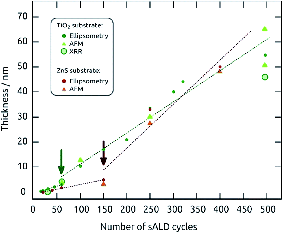 | ||
| Fig. 2 Linear thickness increase of PbS sALD with increasing number of sALD cycles determined by spectroscopic ellipsometry, AFM and XRR. | ||
PbS material characterization
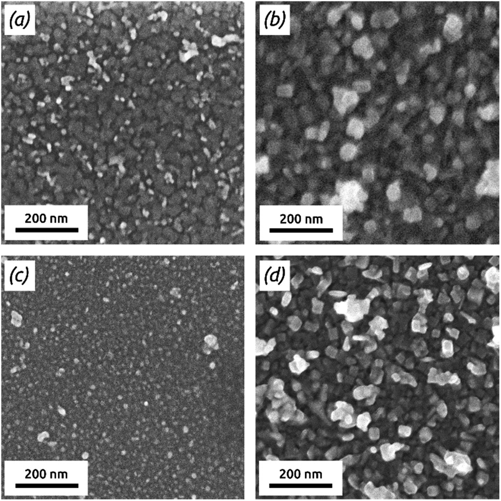 | ||
| Fig. 3 FE-SEM micrographs (top view) of PbS deposited on TiO2 after (a) 45 cycles and (b) 497 cycles and of PbS deposited on ZnS after (c) 40 cycles and (d) 400 cycles. | ||
A quantification of the PbS film roughness is provided by AFM measurements (Fig. S2 and S3 in ESI†). The bare TiO2 surface is smooth (root-mean-square [RMS] roughness 0.4 nm) and displays cracks which result from the annealing procedure of TiO2. After 60 cycles of PbS on TiO2, small particles are spread homogeneously over the TiO2 surface yielding an RMS roughness of 6.0 nm. After 497 cycles, the roughness has increased to 40.9 nm. On the ZnS substrate, the roughness is slightly larger originally (1.3 nm) but increases somewhat more slowly (14.3 nm, 23.5 nm and 28.8 nm after 150, 250 and 400 cycles). The observation of significant roughness is similar to reports of PbS gALD.19,20 The smoother film on ZnS may be related to an improved adhesion compared to oxide substrates.
A further characteristic of ALD is its ability to conformally coat nanostructured surfaces. To demonstrate this capability in the current sALD PbS process, we use deep pores of ‘anodic’ alumina substrates (Fig. 4). The cross-sectional SEM micrograph of an anodic aluminum oxide (AAO) membrane with 5 μm long pores coated with 80 cycles of PbS (in flow-by geometry) exhibits irregularly shaped PbS particles homogeneously deposited throughout the pores (Fig. 4a). Cross-sectional X-ray microanalyses (energy-dispersive X-ray spectroscopy, EDX) along the AAO (20 points spread evenly from bottom to top of the AAO in a distance of approximately 0.4 μm) show the expected Al and O signals of the AAO substrates (and C from the sample holder), plus Pb and S. Their (weak) contributions are approximately constant across the AAO membrane (points 5–15 in Fig. 4b), indicating a homogeneous coating. The PbS material deposited on the top face of the membranes causes locally increased Pb and S signals.
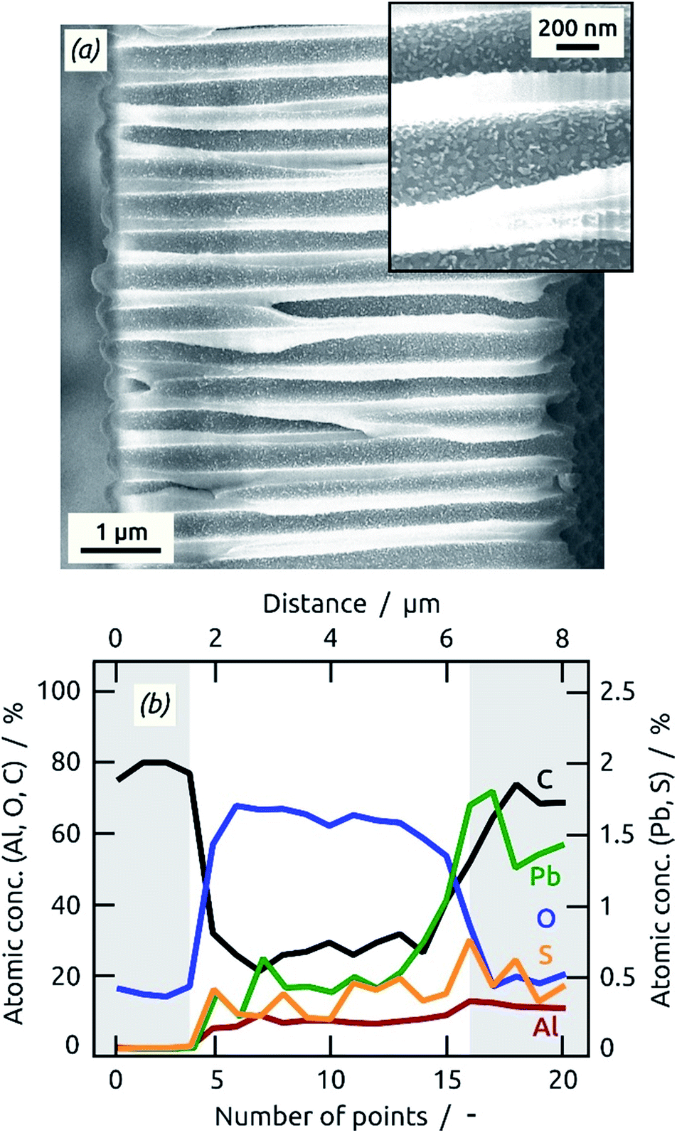 | ||
| Fig. 4 (a) Cross-sectional SEM micrograph of a porous AAO membrane coated with 80 cycles of PbS sALD (with magnified inset). (b) EDX profile of C, O and Al of the AAO membrane as reference and of Pb and S from PbS inside the AAO. The elements Pb and S are present along the whole pore length (the grey sections lie outside the membrane). | ||
![[thin space (1/6-em)]](https://www.rsc.org/images/entities/char_2009.gif) :1 stoichiometry of the elements, although the signals are weak. A more precise determination of the elemental composition is provided by X-ray photoelectron spectroscopy (XPS). Fig. 5 shows XPS survey spectra and Pb 4f and S 2p regions of PbS films (60 and 150 cycles on TiO2). The presence of Ti and O signals for the thinner sample demonstrates that at low coverage the film is discontinuous, in line with the other observations so far. The Pb 4f region displays well-separated spin–orbit components for Pb 4f7/2 and Pb 4f5/2.26 A small contribution of metallic Pb can be found at 136.5 eV and 141.4 eV after 60 cycles,26 but has disappeared after 150 cycles. On the high binding energy side, contributions of oxidized lead at 138.7 eV (Pb 4f7/2) and 143.7 eV (Pb 4f5/2) are found for both samples, albeit less prominently for the thicker one.26,27 The main contribution in all Pb 4f regions, however, results from PbS (137.5 eV and 142.39 eV).27,28 The peak separation energy of 4.9 eV within the spin–orbit pair is in good agreement with the reported value and indicates a strong binding between the Pb(+II) and S(−II) ions.28 The S 2p core level XPS spectra corroborate these observations. The main signals are spin–orbit split at 160.6 eV (S 2p3/2) and 161.9 eV (S 2p1/2).29 The main contribution can be attributed to PbS,27–29 whereas the 60-cycle sample exhibits some oxidation at 168.3 eV.27,30 This oxidation is also visible in the O 1s XPS spectrum (Figure S5†),31–34 and is precedented in the literature for thin PbS films.35 In summary, the XPS data provide evidence for a pure, stoichiometric PbS film which becomes more stable, and therefore less prone to aerobic degradation, as it grows. The oxidized material could be PbO and/or PbSO4. If they are generated by oxidation in air and are not inherent to the sALD film, their presence should become more prominent with aerobic storage time of the samples. This effect can be observed by X-ray diffraction (XRD).
:1 stoichiometry of the elements, although the signals are weak. A more precise determination of the elemental composition is provided by X-ray photoelectron spectroscopy (XPS). Fig. 5 shows XPS survey spectra and Pb 4f and S 2p regions of PbS films (60 and 150 cycles on TiO2). The presence of Ti and O signals for the thinner sample demonstrates that at low coverage the film is discontinuous, in line with the other observations so far. The Pb 4f region displays well-separated spin–orbit components for Pb 4f7/2 and Pb 4f5/2.26 A small contribution of metallic Pb can be found at 136.5 eV and 141.4 eV after 60 cycles,26 but has disappeared after 150 cycles. On the high binding energy side, contributions of oxidized lead at 138.7 eV (Pb 4f7/2) and 143.7 eV (Pb 4f5/2) are found for both samples, albeit less prominently for the thicker one.26,27 The main contribution in all Pb 4f regions, however, results from PbS (137.5 eV and 142.39 eV).27,28 The peak separation energy of 4.9 eV within the spin–orbit pair is in good agreement with the reported value and indicates a strong binding between the Pb(+II) and S(−II) ions.28 The S 2p core level XPS spectra corroborate these observations. The main signals are spin–orbit split at 160.6 eV (S 2p3/2) and 161.9 eV (S 2p1/2).29 The main contribution can be attributed to PbS,27–29 whereas the 60-cycle sample exhibits some oxidation at 168.3 eV.27,30 This oxidation is also visible in the O 1s XPS spectrum (Figure S5†),31–34 and is precedented in the literature for thin PbS films.35 In summary, the XPS data provide evidence for a pure, stoichiometric PbS film which becomes more stable, and therefore less prone to aerobic degradation, as it grows. The oxidized material could be PbO and/or PbSO4. If they are generated by oxidation in air and are not inherent to the sALD film, their presence should become more prominent with aerobic storage time of the samples. This effect can be observed by X-ray diffraction (XRD).
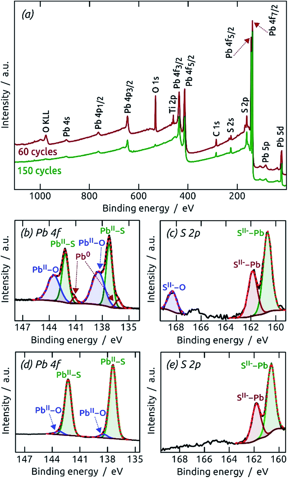 | ||
| Fig. 5 (a) XPS survey spectrum of 60 cycles and 150 cycles PbS sALD on TiO2. Pb 4f (b) and S 2p (c) regions after 60 cycles, Pb 4f (d) and S 2p (e) spectrum after 150 cycles. | ||
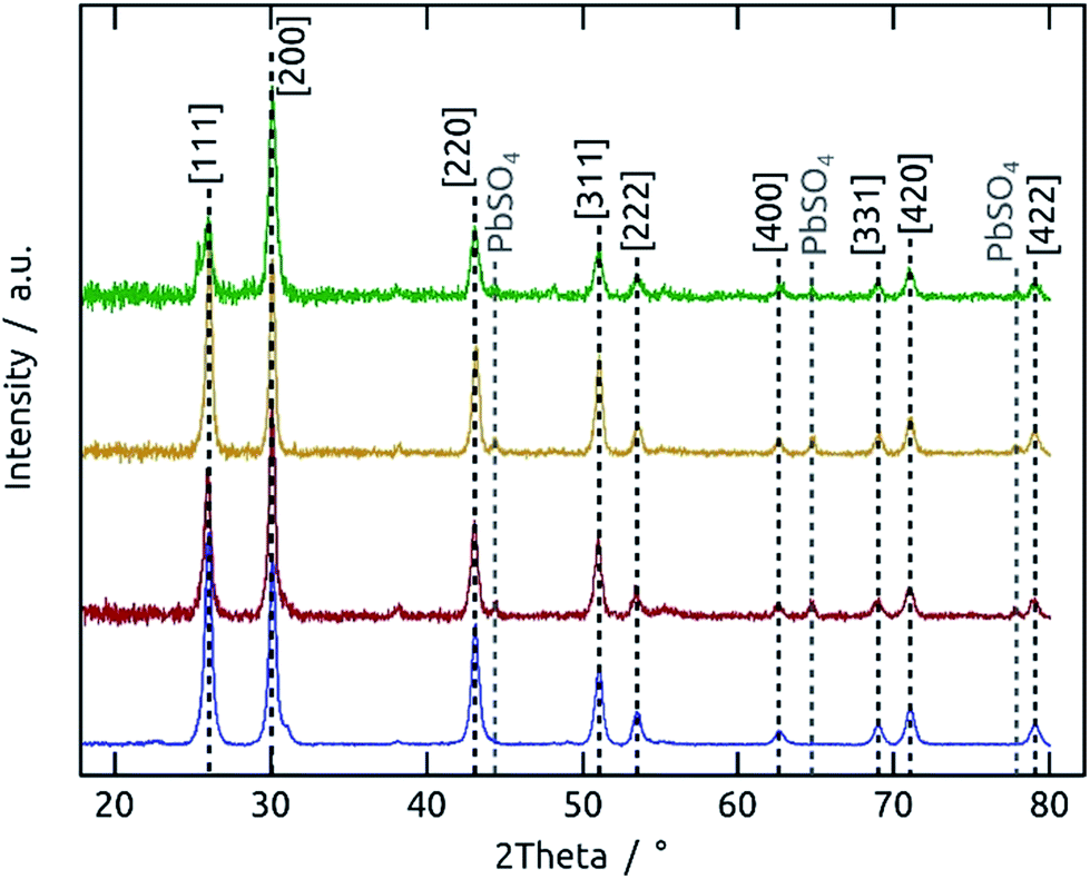 | ||
| Fig. 6 GI-XRD diffractograms of 497 PbS sALD cycles on TiO2 as grown (blue curve), after three weeks of storage in air (red curve) and after annealing at 300 °C for 4 h (orange curve); GI-XRD diffractogram of 400 PbS sALD cycles as grown on ZnS (green curve). | ||
To summarize, the PbS sALD process allows for the direct deposition of polycrystalline PbS on TiO2 and ZnS. The deposited PbS films are stoichiometric and thermally stable at temperatures up to 300 °C, albeit sensitive to aerobic oxidation. In the next step, they can be converted to methylammonium iodoplumbate (MAPI).
Characterization of the MAPI product
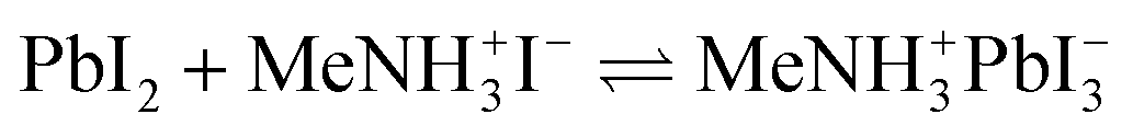
We hypothesize that a related reaction may lead to it from lead sulfide directly, upon generation of gaseous by-products,

Indeed, exposure of a PbS film (497 sALD cycles) coated on TiO2 to the vapors evolved by solid methylammonium iodide at 150 °C (‘vapor annealing’) generates a new crystalline film with GI-XRD peaks at 14.1°, 24.5°, 28.4°, 31.9°, 40.6° and 43.2°, whereas the original signals of PbS have disappeared completely (Fig. 7). The positions of the new peaks are characteristic of the [110], [202], [220], [310], [224] and [314] reflexes of the CH3NH3PbI3 perovskite structure (MAPI, Crystallography Open Database, entry 4335638).9,10,43–45 The small peak at 25.3° can be attributed to the [101] reflex of the underlying anatase TiO2 layer (Crystallography Open Database, entry 9015929) and not to remnants of PbS ([100] reflex at 26.0°) (see also TiO2 reference diffractogram, Fig. S7†). No PbI2 (a likely intermediate product of the reaction as well as the typical decomposition product) is observed.9,43–45
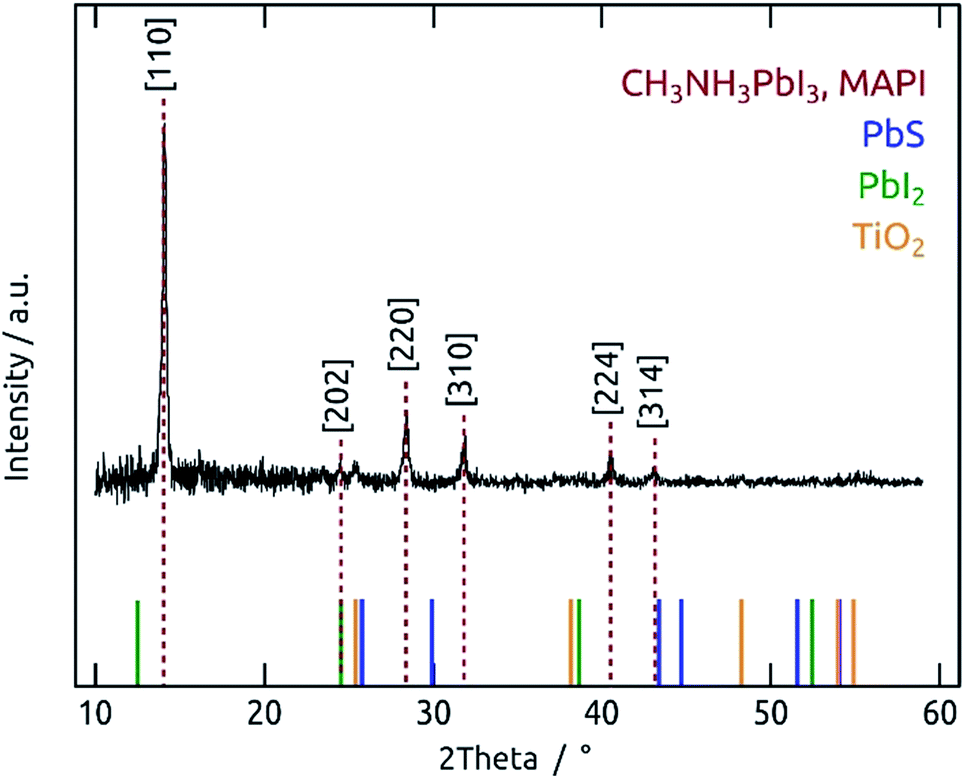 | ||
| Fig. 7 GI-XRD diffractogram of MAPI on TiO2 (converted from 100 cycles of PbS). The peak at 25.3° can be attributed to the anatase TiO2 substrate. | ||
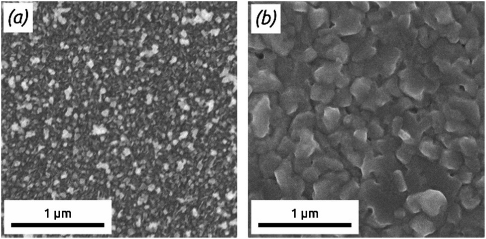 | ||
| Fig. 8 Scanning electron micrographs of (a) 497 cycles PbS before conversion and (b) the same sample after conversion to MAPI. The substrate is TiO2 on a Si/SiO2 wafer. | ||
:I ratio is determined at 1:2.5, compatible within experimental uncertainty with the stoichiometric ratio of 1:3 expected for MAPI. A more precise elemental analysis of MAPI was performed by XPS. Fig. 9a shows the XPS survey spectrum of a similar sample, which exhibits the expected signals for Pb, I, N and C from MAPI and the complete absence of S. Moreover, signals for O and Ti from the TiO2 substrate are detected as well. The Pb 4f and I 3d XPS core level spectra are depicted in Fig. 9b and c (C 1s, N 1s, S 2p and Ti 2p regions as Fig. S13a–d in the ESI†). The Pb 4f region exhibits well separated spin–orbit components for Pb 4f7/2 Pb 4f5/2 at 138.3 eV and 143.2 eV, respectively, close to the values reported for Pb(II) in MAPI.47–49 A small contribution of metallic Pb at 136.9 eV is often observed in MAPI.47 The presence of oxide-bound Pb(II) at 139.0 eV and 143.3 eV may result from the MAPI/TiO2 interface.50,51 The I 3d scan shows two perfect signals for I 3d5/2 and I 3d3/2 at 619.3 eV and 630.8 eV for the iodides.47–49 The high degree of purity that this I 3d region suggests is corroborated by the complete absence of a sulfur signal and the appearance of one species in the N 1s scan associated with the methylammonium ion, which was absent in the PbS starting material (Fig. S5 and S6†).47,49
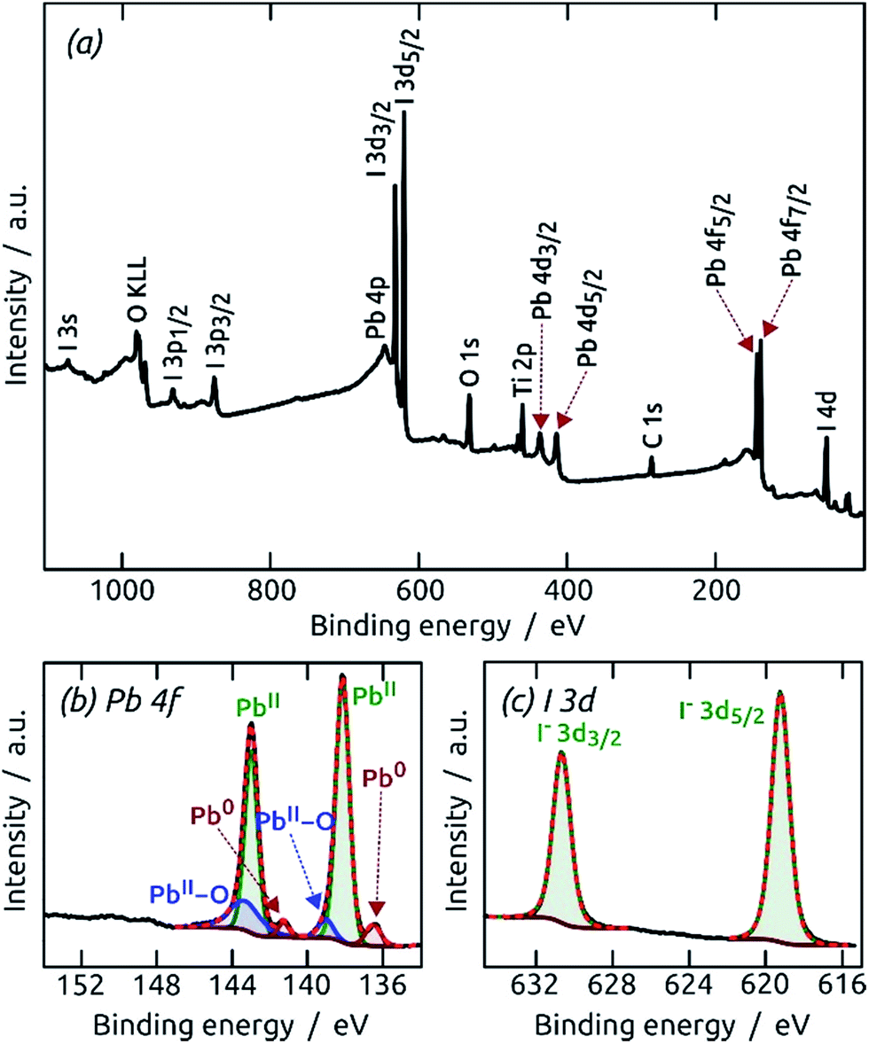 | ||
| Fig. 9 (a) XPS survey spectrum and XPS core level spectra of (b) Pb 4f, (c) C 1s, (d) N 1s and (e) I 3d showing the successful conversion of 100 cycles PbS to MAPI on TiO2. | ||
Conclusions
We provide a novel technique, namely ‘Solution Atomic Layer Deposition’ (sALD), to deposit polycrystalline PbS thin films in a controllable, scalable and conformal manner under mild conditions — room temperature, atmospheric pressure. The ALD (self-limiting) nature of the surface reactions is established. The procedure is applicable not only to planar substrates but also to the uniform coating of deep pores. Cross sectional FE-SEM and EDX measurements prove the coating of the pores with PbS. The exhaustive characterization demonstrates the high purity, stoichiometry, and crystalline quality of the p-type semiconductor. A simple vapor annealing procedure allows one to convert the sALD PbS layer to the hybrid perovskite in one single step. The perovskite is pure (free of PbS and PbI2) and highly crystalline. So far, the procedure has worked equally well for PbS films on planar substrates generated with up to 500 ALD cycles (65 nm PbS or 130 nm MAPI approximately). No porosity is observed which could be generated by degassing, in line with the high mobility of the MAPI solid documented in the literature. Whether an upper thickness limit exists for successful conversion remains to be seen, but is of limited practical relevance since ALD is best suited to thin layers. We have, however, observed that pores of >500 nm depth filled with PbS completely are not converted homogeneously.Our study provides a first foray into an atomic-layer approach to hybrid perovskite semiconductors. This class of ionic solids has long been excluded from the ALD community due to the incompatibility between vacuum processing (typical ALD conditions) and solution processing (suitable for hybrid perovskites). The new solution ALD method provides the unique linchpin between these previously distinct fields of research. Current efforts in our laboratory are dedicated to improving the continuity of the solids, rendering their surfaces less rough, and eradicating pinholes. For this purpose, we are exploring adhesion layers that affect the growth mode and morphology of the deposited PbS, on the one hand, and fine-tuning of the conditions of vapor annealing conversion to MAPI, on the other hand. We expect that smooth MAPI coatings obtained with this sALD strategy on planar and structured substrates can then be incorporated into photovoltaic devices.
Conflicts of interest
There are no conflicts to declare.Acknowledgements
This work was supported by the European Research Council via the ERC Consolidator Grant ‘Solacylin’ (grant agreement 647281) and by the DFG (Deutsche Forschungsgemeinschaft) via the bridge funding of the excellence cluster ‘Engineering of Advanced Materials’ (EAM, EXC315). We thank Dr A. Both Engel for her contribution to XPS and Hall measurements.References
- M. A. Green, Y. Hishikawa, E. D. Dunlop, D. H. Levi, J. Hohl-Ebinger, M. Yoshita and A. W. Y. Ho-Baillie, Prog. Photovoltaics, 2019, 27, 3–12 Search PubMed.
- T. Sherahilo, Oxford PV Sets World Record for Perovskite Solar Cell, Oxford PV, press release on 25 June 2018, https://www.oxfordpv.com/news/oxford-pv-sets-world-record-perovskite-solar-cell, accessed March 2019 Search PubMed.
- Z. Yang, C. C. Chueh, F. Zuo, J. H. Kim, P. W. Liang and A. K. Y. Jen, Adv. Energy Mater., 2015, 5, 1500328 CrossRef.
- M. L. Petrus, J. Schlipf, C. Li, T. P. Gujar, N. Giesbrecht, P. Müller-Buschbaum, M. Thelakkat, T. Bein, S. Hüttner and P. Docampo, Adv. Energy Mater., 2017, 7, 1700264 CrossRef.
- H. Wedemeyer, J. Michels, R. Chmielowski, S. Bourdais, T. Muto, M. Sugiura, M. G. Dennler and J. Bachmann, Energy Environ. Sci., 2013, 6, 67–71 RSC.
- InPassion ALD, SoLayTec, http://www.solaytec.com/products/inpassion-ald, accessed March 2019 Search PubMed.
- Y. Wu, D. Döhler, M. Barr, E. Oks, M. Wolf, L. Santinacci and J. Bachmann, Nano Lett., 2015, 15, 6379–6385 CrossRef CAS PubMed.
- J. Fichtner, Y. Wu, J. Hitzenberger, T. Drewello and J. Bachmann, ECS J. Solid State Sci. Technol., 2017, 6, 171–175 CrossRef.
- W. Li, J. Yang, Q. Jiang, R. Li and L. Zhao, Sol. Energy, 2018, 159, 300–305 CrossRef CAS.
- H. Abbas, R. Kottokkaran, B. Ganapathy, M. Samiee, L. Zhang, A. Kitahara, M. Noack and V. L. Dalal, APL Mater., 2015, 3, 016105 CrossRef.
- W. A. Laban and L. Etgar, Energy Environ. Sci., 2013, 6, 3249–3253 RSC.
- J. M. C. Da Silva Filho, V. A. Ermakov and F. C. Marques, Sci. Rep., 2018, 8, 838–845 CrossRef PubMed.
- A. Rogalski, Opto-Electron. Rev., 2012, 20, 279–308 Search PubMed.
- N. Ajayakumar, C. O. Sreekala, A. E. Tom, A. Thomas and V. V. Ison, Presented in parts at International Conference on Electrical, Electronics, and Optimization Techniques (ICEEOT), Chennai, India, March 2016 Search PubMed.
- B. Scharifker, Z. Ferreira and J. Mozota, Electrochim. Acta, 1985, 30, 677–682 CrossRef CAS.
- N. S. Al Din, N. Hussain and N. Jandow, AIP Conf. Proc., 2016, 1758, 020002 CrossRef.
- T. Kanniainen, S. Lindroos, J. Ihanus and M. Leskelä, J. Mater. Chem., 1996, 6, 161–164 RSC.
- J. Puišo, S. Lindroos, S. Tamulevičius, M. Leskelä and V. Snitka, Thin Solid Films, 2003, 428, 223–226 CrossRef.
- E. Nykänen, J. Laine-Ylijoki, P. Soininen, L. Niinistö, M. Leskelä and L. G. Hubert-Pfalzgraf, J. Mater. Chem., 1994, 4, 1409–1412 RSC.
- N. P. Dasgupta, W. Lee and F. B. Prinz, Chem. Mater., 2009, 21, 3973–3978 CrossRef CAS.
- T. P. Brennan, O. Trejo, K. E. Roelofs, J. Xu, F. B. Prinz and S. F. Bent, J. Mater. Chem. A, 2013, 1, 7566 RSC.
- P. K. Afonicheva and L. B. Matyushkin, Presented in parts at IEEE NW Russia Young Researchers in Electrical and Electronic Engineering Conference (EIConRusNW), St. Petersburg, Russia, February 2016 Search PubMed.
- J. Choi, S. Song, M. T. Hörantner, H. J. Snaith and T. Park, ACS Nano, 2016, 10, 6029–6036 CrossRef CAS PubMed.
- R. L. Puurunen, J. Appl. Phys., 2005, 97, 121301 CrossRef.
- L. S. Chongad, A. Sharma, M. Banerjee and A. Jain, J. Phys.: Conf. Ser., 2016, 755, 012032 CrossRef.
- XPS Interpretation of Lead, Thermo Fisher Scientific Inc, https://xpssimplified.com/elements/lead.php, accessed February 2019 Search PubMed.
- D. J. H. Cant, K. L. Syres, P. J. B. Lunt, H. Radtke, J. Treacy, P. J. Thomas, E. A. Lewis, S. J. Haigh, P. O'Brien and K. Schulte, Langmuir, 2015, 31, 1445–1453 CrossRef CAS PubMed.
- V. V. Burungale, R. S. Devan, S. A. Pawar, N. S. Harale, V. L. Patil, V. K. Rao, Y. R. Ma, J. E. Ae, J. H. Kim and P. S. Patil, Mater. Sci.-Pol., 2016, 34, 204–211 CAS.
- XPS Interpretation of Sulphur, Thermo Fisher Scientific Inc, https://xpssimplified.com/elements/sulfur.php, accessed February 2019 Search PubMed.
- M. Nam, T. Lee, S. Kim, S. Kim, S.-W. Kim and K. K. Lee, Org. Electron., 2014, 15, 391–398 CrossRef CAS.
- M. C. Biesinger, L. W. M. Lau, A. R. Gerson and R. S. C. Smart, Appl. Surf. Sci., 2010, 257, 887–898 CrossRef CAS.
- XPS Interpretation of Oxygen, Thermo Fisher Scientific Inc, https://xpssimplified.com/elements/oxygen.php, accessed March 2019 Search PubMed.
- T. Singh, S. Öz, A. Sasinska, R. Frohnhoven, S. Mathur and T. Miyasaka, Adv. Funct. Mater., 2018, 28, 1706287 CrossRef.
- B. Bharti, S. Kumar, H. N. Lee and R. Kumar, Sci. Rep., 2016, 6, 32355 CrossRef CAS PubMed.
- A. S. Manocha and R. L. Park, Appl. Surf. Sci., 1977, 1, 129–141 CrossRef CAS.
- L. S. Ramsdell, Am. Mineral., 1925, 10, 281–304 CAS.
- C. Song, M. Sun, Y. Yin, J. Xiao, W. Dong, C. Li and L. Zhang, Mater. Res., 2016, 19, 1351–1355 CrossRef CAS.
- W. Liu, B. Ma, F. Li, Y. Fu, J. Tai, Y. Zhou and L. Lei, RSC Adv., 2016, 6, 108513–108522 RSC.
- J. O. Rivera-Nieblas, J. Alvarado-Rivera, M. C. Acosta-Enríquez, R. Ochoa-Landin, J. Espinoza-Beltrán, A. Apolinar-Iribe, M. Flores-Acosta, A. De León and S. J. Castillo, Chalcogenide Lett., 2013, 10, 349–358 CAS.
- F. Gode, O. Baglayan and E. P. Guneri, Chalcogenide Lett., 2015, 12, 519–528 CAS.
- E. M. Nasir and M. M. Abass, Chalcogenide Lett., 2016, 13, 271–279 Search PubMed.
- J. F. Woods, Phys. Rev., 1956, 106, 235–240 CrossRef.
- K. Liang, D. B. Mitzi and M. T. Prikas, Chem. Mater., 1998, 10, 403–411 CrossRef CAS.
- A. Bahtiar, S. Rahmanita and Y. D. Inayatie, IOP Conf. Ser.: Mater. Sci. Eng., 2017, 196, 012037 Search PubMed.
- X. Zhang, J. Ye, L. Zhu, H. Zheng, G. Liu, X. Liu, B. Duan, X. Pan and S. Dai, Nanoscale, 2017, 9, 4691 RSC.
- Periodic Table of Elements and X-ray Energies, Bruker, www.bruker.com/fileadmin/user_upload/8-PDF-Docs/X-rayDiffraction_ElementalAnalysis/HH-XRF/Misc/Periodic_Table_and_X-ray_Energies.pdf, accessed February 2019 Search PubMed.
- C. Das, M. Wussler, T. Hellmann, T. Mayer and W. Jaegermann, Phys. Chem. Chem. Phys., 2018, 20, 17180–17187 RSC.
- Z. Hawash, S. R. Raga, D. Y. Son, L. K. Ono, N. G. Park and Y. Qi, J. Phys. Chem. Lett., 2017, 8, 3947–3953 CrossRef CAS PubMed.
- L. Liu, J. A. Mcleod, R. Wang, P. Shen and S. Duhm, Appl. Phys. Lett., 2015, 107, 061904 CrossRef.
- H. S. Potdar, S. D. Sathaye, A. B. Mandale and S. K. Date, Mater. Lett., 1990, 9, 71–76 CrossRef CAS.
- Y. K. Kim, B. Jeon and H. J. Park, J. Phys. Chem. C, 2016, 120, 22460–22465 CrossRef CAS.
Footnote |
| † Electronic supplementary information (ESI) available: Experimental section and additional figures as described in the text. See DOI: 10.1039/c9ta09715e |
| This journal is © The Royal Society of Chemistry 2019 |