
 Open Access Article
 This Open Access Article is licensed under a
 Creative Commons Attribution 3.0 Unported Licence
Spontaneous enhancement of the stable power conversion efficiency in perovskite solar cells†
Somayeh
Moghadamzadeh
 *ab,
Ihteaz M.
Hossain
ab,
Marius
Jakoby
ab,
Bahram
Abdollahi Nejand
ab,
Diana
Rueda-Delgado
a,
Jonas A.
Schwenzer
b,
Saba
Gharibzadeh
ab,
Tobias
Abzieher
b,
Motiur Rahman
Khan
a,
Amir A.
Haghighirad
c,
Ian A.
Howard
ab,
Bryce S.
Richards
ab,
Uli
Lemmer
abd and
Ulrich W.
Paetzold
*ab
*ab,
Ihteaz M.
Hossain
ab,
Marius
Jakoby
ab,
Bahram
Abdollahi Nejand
ab,
Diana
Rueda-Delgado
a,
Jonas A.
Schwenzer
b,
Saba
Gharibzadeh
ab,
Tobias
Abzieher
b,
Motiur Rahman
Khan
a,
Amir A.
Haghighirad
c,
Ian A.
Howard
ab,
Bryce S.
Richards
ab,
Uli
Lemmer
abd and
Ulrich W.
Paetzold
*ab
aLight Technology Institute, Karlsruhe Institute of Technology, Engesserstrasse 13, 76131 Karlsruhe, Germany. E-mail: somayeh.moghadamzadeh@kit.edu; ulrich.paetzold@kit.edu
bInstitute of Microstructure Technology, Karlsruhe Institute of Technology, Hermann-von-Helmholtz-Platz 1, 76344 Eggenstein-Leopoldshafen, Germany
cInstitute for Solid-State Physics, Karlsruhe Institute of Technology, Hermann-von-Helmholtz-Platz 1, D-76021 76344 Eggenstein-Leopoldshafen, Germany
dInnovationLab GmbH, Speyererstrasse 4, 69115 Heidelberg, Germany
First published on 21st November 2019
Abstract
The power conversion efficiency (PCE) of lead-halide perovskite solar cells (PSCs) is reported to increase over a period of days after their fabrication while they are stored in the dark. The effects underlying this spontaneous enhancement thus far are not understood. This work investigates the phenomenon for a variety of multi-cation-halide PSCs with different perovskite compositions and architectures. The observations reveal that spontaneous enhancement is not restricted to specific charge transport layers or perovskite compositions. The highest PCE observed in this study is an enhanced stable PCE of 19% (increased by 4% absolute). An increased open-circuit voltage is the primary contributor to the improved efficiency. Using time-resolved photoluminescence measurements, the initially present low-energy states are identified which disappear over a storage period of a few days. Furthermore, trap states probed by the thermally stimulated current technique exist in pristine PSCs and strikingly decrease for stored devices. In addition, the ideality factor approaches unity and X-ray diffraction analyses show lattice strain relaxation over the same period of time. These observations indicate that spontaneous enhancement of the PCE of PSCs is based on a reduction in trap-assisted non-radiative recombination possibly due to strain relaxation. Considering the demonstrated generality of spontaneous enhancement for different compositions of multi-cation-halide PSCs, our results highlight the importance of determining the absolute PCE increase initiated by spontaneous enhancement for developing high-efficiency PSCs.
1. Introduction
With a record power conversion efficiency (PCE) of 25.2%, hybrid organic-inorganic metal halide perovskite solar cells (PSCs) are among the most-promising technologies for next generation photovoltaics.1 PSCs can be processed from inexpensive precursor materials using a variety of fabrication methods, ranging from vacuum-based2,3 to solution-based4 methods. To optimize and improve the stability of PCEs, a large diversity of perovskite materials and strategies have been developed, ranging from mono- to multi-cation-halides.5–8 Despite the tremendous advances in technology, there are still a number of device-relevant effects that are subject to ongoing investigations. These effects include light soaking,9 light-activated degradation,10–12 ferroelectric domain walls,13,14 and spontaneous enhancement of the PCE.15–18 The latter term refers to the enhancement of the PCE of PSCs a few days after device fabrication, if the devices are stored in the dark.In terms of the spontaneous enhancement, several research groups have reported that the PCE of multi-cation-halide PSCs reaches its highest value after a few days of storage in the dark after device fabrication.15–19 In addition to multi-cation-halide PSCs, a few studies reported the same phenomenon for MAPbI3.16–18 There are various hypotheses for the explanation of this phenomenon in the literature.15–18 A recent study attributed the spontaneous enhancement to improved crystallinity in addition to released residual stress and lattice distortion over long-term storage, which was ascertained by an observed increase in the peak intensity and a shift to the higher diffraction angles in the X-ray diffraction (XRD) pattern.16 A spontaneous coalescence of smaller crystallites within perovskite thin films into larger ones is another hypothesis in the literature.15–17 The coalescence leads to a reduction in the number of grain boundaries and consequently a reduction in non-radiative recombination occurring at the grain boundaries.
Another study determined a gradual diffusion of sodium (Na+) ions from the indium tin oxide (ITO) glass substrate into the perovskite thin film. This diffusion initiates a spontaneous passivation which leads to a reduction of trap density of states at the grain boundaries of perovskite thin films during the storage time period and ultimately better performance.18 Overall, yet no consensus has been reached on the origin of the spontaneous enhancement and a systematic experimental comparison of architectures and perovskite compositions to ascertain the generality of the spontaneous enhancement and its underlying causes is missing.
This work aims to provide such a systematic study on the spontaneous enhancement of photovoltaic performance of multi-cation-halide PSCs. We investigate a variety of perovskite thin films with different cation and halide compositions, including methylammonium (MA)-free perovskites [Cs0.17FA0.83Pb(I0.83Br0.17)3], cesium (Cs)-free perovskites [FA0.83MA0.17Pb(I0.83Br0.17)3], and Cs-containing perovskites [Csx(FA0.83MA0.17)(1−x)Pb(I0.83Br0.17)3], with x = 0.05, 0.1, and 0.15 and [Cs0.1(FA0.83MA0.17)0.9Pb(I0.67Br0.33)3]. We also vary the device architecture using different electron transport layers (ETLs), including TiO2 nanoparticles (np-TiO2), C60 (deposited on top of the np-TiO2 layer), and SnO2 nanoparticles (np-SnO2). We find that the spontaneous enhancement is general, occurring in all these cases; however, PSCs with poor initial PCEs exhibit more prominent enhancement in comparison to PSCs with high initial efficiencies. We perform optical spectroscopy and XRD measurements and characterize the ideality factor in order to investigate the causes of the spontaneous enhancement. Time-resolved photoluminescence (PL) spectra collected at different time delays after excitation of the perovskite thin films reveal the existence of lower-energy states next to the bulk bandgap phase with 80 meV difference on the day of sample preparation. However, after storing the sample for a few days, the lower-energy states disappear and only the peak of the bulk bandgap phase remains. A similar effect is observed in thermally stimulated current (TSC) measurements where the density of trap states close to the bandgap is drastically reduced during storage time. These observations are consistent with the improved open-circuit voltage (VOC) of the corresponding PSCs, the increased carrier lifetime, and the ideality factor approaching unity after storage. Furthermore, XRD analyses reveal a reduction in the strain in the perovskite thin films.
2. Results and discussion
2.1. Reference case: spontaneous enhancement of the stable power conversion efficiency
We fabricated reference PSCs in an inert atmosphere (N2-filled glovebox) using a triple cation perovskite thin film with the composition Cs0.1(FA0.83MA0.17)0.9Pb(I0.83Br0.17)3, hereafter referred to as Cs0.1FM0.9. The layer sequence of the PSC is glass/ITO/np-TiO2/Cs0.1FM0.9/2,2′,7,7′-tetrakis[N,N-di(4-methoxyphenyl)amino]-9,9′-spirobifluorene (spiro-MeOTAD)/gold (Au). The experimental section provides a detailed explanation regarding device fabrication. As shown in Fig. 1a, the PCE of a Cs0.1FM0.9 solar cell, being measured for 300 s at constant voltage close to the maximum power point (MPP), is low (<13%) and does not stabilize on the day of sample preparation (day 1). However, after storing the same device at room temperature in the dark and in an inert atmosphere for a few days, the PCE gradually increases and stabilizes at 16% on day 10 and 17% on day 40. Importantly, even after an extended period of time, the stable PCE reaches 17.5% on day 150. Interestingly, the same sample shows a stable PCE of 16.6% on day 785, with 1% absolute loss due to possible degradation after a long-term storage in the dark (compare Fig. 1a). The current-density–voltage (J–V) characteristics for the same device, given in Fig. 1b, demonstrate that the key PV characteristic that improves during the storage period is VOC. It increases from 1.13 V on day 1 (with a PCE of 16.7%) to 1.19 V on day 40 (with a PCE of 18%). A VOC of 1.19 V is remarkable for single junction PSCs with a band gap of 1.62 eV. | ||
| Fig. 1 (a) Power conversion efficiency (PCE) measured for 300 s at constant voltage close to the maximum power point (MPP), and (b) current-density–voltage (J–V) characteristics of a Cs0.1(FA0.83MA0.17)0.9Pb(I0.83Br0.17)3 solar cell (Cs0.1FM0.9), measured on the day of sample preparation (day 1) and several days after storage. We measure the J–V characteristics at a fixed rate of 0.6 V s−1 from open-circuit voltage (VOC) to short-circuit current (JSC) (solid lines) and from JSC to VOC (dashed lines) under air-mass 1.5 global (AM1.5 G) spectra (100 mW cm−2, 25 °C). (c) PCE after 5 min measured at constant voltage close to the MPP (PCEafter 5 min) derived from 16 identically prepared Cs0.1FM0.9 solar cells. Open symbols indicate that the power output does not stabilize over 5 min. (d) Calculated hysteresis index of 40 identically prepared Cs0.1FM0.9 solar cells (HI = AFW/ABW), where AFW and ABW are the areas under forward and backward scans in the J–V characteristics, respectively. The HI of 1 presents a PSC without hysteresis and lower values of the HI are indicative of more pronounced hysteresis. | ||
As shown in Fig. 1c, the PCE after 5 min measured at constant voltage close to the MPP (PCEafter 5 min), derived from 16 identically prepared Cs0.1FM0.9 solar cells, improves significantly from <10% on day 1 to ∼17% on day 40 on average. Moreover, along with the spontaneous enhancement of the stable power output, we found the hysteresis index (HI) to decrease over time (see Fig. 1d). This is in agreement with the increased stability of the solar cell power output, since a low hysteresis and stable power output are often – not always – correlated.20 The J–V parameters derived from 40 identically prepared Cs0.1FM0.9 solar cells aged up to 40 days are provided in Fig. S1.†
2.2. Role of the perovskite compositions
The nature of the cations and halides as well as the metal anion in the multi-cation-halide perovskite structure is known to impact the optoelectronic properties and stability of these PSCs. For example, the incorporation of Cs has been reported to cause a reduction in trap density in the bulk or at the grain boundaries of the perovskite material and the charge recombination rate.21,22 Here, we investigate whether and how the spontaneous enhancement of the PCE is affected by changing the ratio of Cs from x = 0, to 0.05, 0.1, and 0.15 in Csx(FA0.83MA0.17)(1−x)Pb(I0.83Br0.17)3. All the PSCs are processed on the np-TiO2 ETL under identical conditions. As presented in Fig. 2, irrespective of the Cs concentration in the investigated range, the average value of the PCEafter 5 min for all samples increases in the range 4.2–6% (absolute average) over a ten-day period of storage. We also observe the same behavior in performance of PSCs with a double cation perovskite [Cs0.17FA0.83Pb(I0.83Br0.17)3] with a bandgap of EG ∼ 1.63 eV and a triple cation perovskite [Cs0.1(FA0.83MA0.17)0.9Pb(I0.67Br0.33)3] with a bandgap of EG ∼ 1.73 eV (see Fig. S2†). Therefore, we conclude that the reported spontaneous enhancement of performance is not limited to a specific composition of the multi-cation-halide perovskite, but a general effect for different compositions of the large cations and halide anions in the perovskite crystal structure. This conclusion is also supported by the literature observations wherein the phenomenon has also been reported for MAPbI3 and Pb-free PSCs.16,17,19 | ||
| Fig. 2 Power conversion efficiency after 5 min measured at constant voltage close to the maximum power point (PCEafter 5 min), derived from 16 Csx(FA0.83MA0.17)(1−x)Pb(I0.83Br0.17)3 solar cells, where x is the ratio of Cs. We measure the devices on the day of sample preparation (day 1) and after storage (day 10). Open symbols indicate that the power output does not stabilize over 5 min. ΔPCEave corresponds to the average enhancement of the power conversion efficiency (PCE) of the perovskite solar cells compared to that on day 1. | ||
2.3. Role of the electron transport layer
Having demonstrated that the current reported spontaneous enhancement of performance occurs for a variety of compositions of multi-cation-halide PSCs, we now investigate whether it is correlated to the choice of the ETL. In general, the electron charge transport layer impacts the morphology of perovskite thin films and also affects the energy level alignment; this is critical for electron charge extraction, as well as hole blocking and consequently for photovoltaic performance of PSCs.23–26 PSCs comprising fullerene (C60) and its derivatives (PCBM, ICBA, etc.) are reported to be less influenced by ion migration and trap-assisted recombination at the ETL/perovskite interface and therefore show low hysteresis.27–29 In planar PSCs, the SnO2 ETL is widely used, given its improved stability under ultraviolet (UV) illumination30,31 and very good electron extraction in PSCs.32We investigate the reported spontaneous enhancement of the PCE of Cs0.1FM0.9 solar cells prepared on three different ETLs; np-TiO2, C60 (deposited on top of the np-TiO2 layer), and np-SnO2. As shown in Fig. 3a, the average value of the PCEafter 5 min improves by at least 2.5% absolute after storing the devices for 10 days, in a similar way independent of the ETL. Although the spontaneous enhancement is neither restricted to the choice of the ETL nor the compositions of the perovskite, the degree of the enhancement varies for PSCs prepared on different ETLs. This could be correlated to the different morphology of the perovskite thin film, which relies strongly on the substrate. In general, we observe that devices with high PCEs show less enhancement while devices with low PCEs exhibit prominent spontaneous enhancement, as also reported elsewhere.15 Additionally, as shown in Fig. S3a,† the PCE of a pristine Cs0.1FM0.9 solar cell with a np-SnO2 ETL stabilizes even on day 1 and gradually enhances from ∼16% to ∼18.5% on day 50. Fig. S3b† shows the PCEafter 5 min values of 12 identically prepared Cs0.1FM0.9 solar cells with np-SnO2 ETLs over time with the highest value of ∼19% after 50 days. Fig. S4† presents the J–V parameters for these solar cells over time, with the highest PCE of ∼19.6% (which is respectable for solvent-quenched triple-cation based PSCs),21,33 a VOC of ∼1.14 V, a JSC of ∼22.3 mA cm−2, and a FF of ∼77% after 50 days for the champion cell. We also observe that the spontaneous enhancement not only occurs for device architectures that exhibit pronounced hysteresis. As presented in Fig. 3b, incorporating C60 onto np-TiO2 substrates decreases the hysteresis of pristine devices but it does not affect the overall spontaneous performance enhancement of these solar cells.
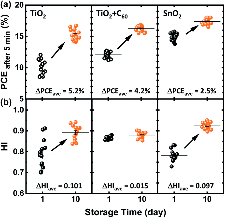 | ||
| Fig. 3 (a) Power conversion efficiency after 5 min measured at constant voltage close to the maximum power point (PCEafter 5 min), derived from 16 Cs0.1(FA0.83MA0.17)0.9Pb(I0.83Br0.17)3 solar cells with various electron transport layers, measured on the day of sample preparation (day 1) and after storage (day 10). Open symbols indicate that the power output does not stabilize over 5 min. (b) Calculated hysteresis index (HI) for the same PSCs on the same days. ΔPCEave and ΔHI correspond to the average enhancement of the power conversion efficiency and HI of the perovskite solar cells compared to those on day 1, respectively. | ||
In summary, these findings indicate that the observed spontaneous enhancement of the stable power output is neither limited to a specific ETL nor to the ETL/perovskite interface itself. The latter is reported to induce a number of issues such as surface defects originating from the oxygen vacancies activated under UV illumination in the case of using TiO2 as the ETL, interfacial trap states and accumulation of the charges.34 These issues result in non-radiative recombination and reduced charge transfer at this interface.35–40
2.4. Role of the hole transport layer; spiro-MeOTAD
After investigating the role of the ETL and the composition of the perovskite material, we now examine the impact of the hole transport layer (HTL). Doped organic HTLs have been reported to affect the stability of PSCs.41,42 In particular, spiro-MeOTAD with the highly diffusive additives Li-TFSI and 4-tert-butylpyridine (4-tBP) affects the hysteresis and stability of PSCs if exposed to external stress factors like light, temperature and/or an external bias voltage.41,42 This dependency between the stability of the PSC and the spiro-MeOTAD HTL motivates the following investigation on the role of spiro-MeOTAD as the HTL in the spontaneous enhancement of PSC performances. For this purpose, we compare the performance enhancement of Cs0.1FM0.9 solar cells, by varying the time interval between the deposition of the perovskite thin film and the deposition of doped spiro-MeOTAD as the HTL and Au as the back contact (see Fig. S5†). In this way, we can discriminate whether the spontaneous enhancement of the stable power output occurs independent of the presence of doped spiro-MeOTAD. As mentioned before, the power output of devices with np-TiO2 or np-TiO2/C60 ETLs stabilizes gradually over a timescale of a few days, while it stabilizes on the first day of device preparation in the case of using the np-SnO2 ETL. In order to avoid additional complexity concerning the stability of devices, we employ np-SnO2 as the ETL here in the following.First, on day 1, we fabricate samples with two different stacks: one, ITO/np-SnO2/Cs0.1FM0.9/spiro-MeOTAD/Au, referred to as category IS (immediate spiro-MeOTAD deposition), and two, ITO/np-SnO2/Cs0.1FM0.9, referred to as category DS (delayed spiro-MeOTAD deposition). Second, we determine the stable PCE of the PSCs of category IS on day 1 and every day after storage in the dark and in an inert atmosphere. Meanwhile, we store the samples of category DS under the same conditions. As exhibited in Fig. 4a, we observe a considerable improvement for PSCs of category IS on day 5. On day 6, we deposit spiro-MeOTAD on the samples of category DS and leave them for overnight oxygen doping in dry air (relative humidity < 35%). On day 7, we complete these samples after evaporating Au and start determining their stable PCEs. The study reveals that the PSCs of category DS immediately exhibit a high stable power output (see Fig. 4a and b). As shown in Fig. S6,† the improvement in all parameters extracted from the J–V measurements for PSCs of category DS is comparable to that of PSCs of category IS. It is noticeable that the VOC and fill factor (FF) are the parameters dominating the PCE enhancement over time. This experiment leads to the conclusion that the spontaneous enhancement of the stable power output does not rely on the presence of an HTL and an electrode or the specific characteristics of doped spiro-MeOTAD.
 | ||
| Fig. 4 (a) Power conversion efficiency after 5 min (PCEafter 5 min) measured at constant voltage close to the maximum power point (MPP), derived from 10 Cs0.1(FA0.83MA0.17)0.9Pb(I0.83Br0.17)3 solar cells with (white background) immediately deposited spiro-MeOTAD layers (IS) and (grey background) 6 day-delayed deposited spiro-MeOTAD layers (DS). (b) Spontaneous enhancement of the power conversion efficiency over time measured at constant voltage close to the MPP derived from the champion perovskite solar cells of category IS and DS. | ||
In summary, based on the above-reported systematic study on the role of different layers in the spontaneous enhancement of the stable power output of multi-cation-halide PSCs, we conclude that the effect originates mostly from the perovskite thin film itself. Neither the HTL nor the ETL significantly influences the effect. In the following sections, we systematically investigate the possible causes by studying the photo-physics and morphology of the perovskite thin film under storage in the dark and in an inert atmosphere.
2.5. Reduced non-radiative losses and enhanced charge carrier lifetime
As shown previously, the spontaneous enhancement of the PCE of Cs0.1FM0.9 solar cells is mainly driven by improvements in the VOC and FF (see Fig. S1, S4, and S6†). The VOC and FF of solar cells are closely related to the ratio of band-to-band radiative recombination as well as non-radiative Shockley–Read–Hall (SRH) recombination in the bulk of perovskite thin film and/or non-radiative recombination at surface defects occurring at grain boundaries and interfaces.43–46 Identifying the ideality factor (nid) is a reliable way to indicate the dominant recombination mechanism in a solar cell.47–49 If nid = 1, radiative recombination and/or surface recombination dominates in the device, whereas if nid = 2, trap-assisted bulk SRH recombination is usually dominant. Recently, Tress et al. summarized that the ideality factor of PSCs is most reliably obtained by light-intensity-dependent VOC measurements.49 For these measurements, one can evaluate nid by a linear fit of the VOCvs. log-scaled light intensity using the equation | (1) |
 | ||
| Fig. 5 V OC vs. light intensity (I) measurements derived from a Cs0.1(FA0.83MA0.17)0.9Pb(I0.83Br0.17)3 solar cell with (a) np-TiO2 and (b) np-SnO2 electron transport layers, measured on the day of sample preparation (day 1) and after storage (day 5, 10). Dashed lines show a linear fit and the numbers indicate the ideality factor (nid) deduced from the slopes using eqn (1). | ||
To provide more insight into the charge recombination properties with regard to the spontaneous enhancement of the PSC performance, we track the steady-state PL spectra and time-resolved PL kinetics of perovskite thin films over the first 10 days after fabrication. In order to avoid charge carrier quenching, the perovskite thin films are prepared on bare glass without charge transport layers. Fig. 6a and b show the corresponding steady-state spectra and time-resolved PL kinetics collected at an excitation fluence of 30 nJ cm−2 on the day of sample fabrication (day 1) and after a ten-day period of storage (day 10) in the dark and in an inert atmosphere. We verify that no fluence dependence is present at this excitation density (compare Fig. S7†). We observe a two-fold stronger PL intensity and a significantly enhanced charge carrier lifetime for the perovskite thin film fabricated on bare glass after 10 days of storage. The increase in the PL intensity and the charge carrier lifetimes indicates a reduction in non-radiative recombination.
 | ||
| Fig. 6 (a) Steady-state photoluminescence (PL) spectra, (b) normalized time-resolved PL kinetics, and (c) time-resolved PL spectra (normalized to peak A) integrated in a time delay between 100 ns and 600 ns after the excitation pulse for a perovskite thin film with the composition Cs0.1(FA0.83MA0.17)0.9Pb(I0.83Br0.17)3 deposited on bare glass. The data are collected on the day of sample preparation (day 1) and after storage (day 10). | ||
Upon repeating the PL analyses on perovskite thin films deposited on ITO/np-TiO2 and ITO/np-SnO2 layers, we observe a similar trend as that on glass (see Fig. S8†). In both cases the PL intensity and carrier lifetime increase over time, although the increase in the PL intensity and PL lifetime after the storage period is more notable for the perovskite thin films deposited on np-TiO2 compared to those deposited on np-SnO2 layers. This observation agrees with the degree of spontaneous enhancement in the stable PCE of the PSCs with the np-TiO2 ETL and np-SnO2 ETL, respectively (compare Fig. 3a). Considering the photovoltaic improvement in the performance of PSCs over time, this increase in the PL intensity in the presence of the ETLs is indicative of a reduction in trap-assisted recombination in the bulk of the perovskite. The suppressed recombination explains the increased VOC, FF, and consequently the increased PCE of the PSCs and is consistent with the ideality factor analysis, as reported in previous sections. It is also worth mentioning that, as shown in Fig. S9,† the PL intensity derived from the samples stored with and without doped spiro-MeOTAD exhibits a comparable improvement independent of the presence of the spiro-MeOTAD layer, which is in agreement with the results discussed in the previous section (see Fig. S6†).
2.6. Appearance of “low-energy states” in pristine perovskite thin films
Via closer examination of the PL spectrum on the day of sample preparation (day 1), we notice a peak appearing at around 800 nm. As shown in Fig. 6c, the delayed emission spectrum of the perovskite thin film – integrated from 100 to 600 ns after excitation – reveals the coexistence of two distinct emission peaks at 763 nm (peak A) and 804 nm (peak B) for the pristine perovskite thin film on day 1. However, after a storage period of 10 days, the same measurement shows that the intensity of peak A increases while the intensity of peak B significantly decreases.To identify the positions and widths of these two peaks, we perform a quantitative analysis of the data. As a starting point, we convert the PL spectra from the original wavelength-scaled to the energy-scaled PL spectra (see Fig. 7) using a Jacobian transformation: E = hc/λ and f(E) ∼ λ2f(λ).50 We globally fit the PL spectra of day 1 and 10 with two-peak pseudo-Voigt profiles (see the ESI†), wherein the peak positions, widths, and contribution factor are shared between fitting profiles used for day 1 and 10, whereas the area is allowed to change. Upon fitting with a pseudo-Voigt profile, we find the positions of the two peaks on day 1 to be at 1.54 eV and 1.62 eV. However, after 10 days, the peak at 1.54 eV almost disappears and the intensity of the peak at 1.62 eV, which according to the literature is very close to the bulk bandgap of triple cation perovskite materials, increases.21 Considering that PL is highly sensitive to sub-bandgap states which are filled by energy relaxation, the existence of the observed low-energy states would be sufficient to considerably alter the PL. Based on the values we obtain from the fitting for the relative areas under these two peaks on different days (see Table S1†), we find that 66% of the emission comes from the lower-energy peak on day 1, whereas only 21% of the total emission comes from the same peak on day 10. This reduction of the lower-energy peak is attributed to either a reduction in the density of shallow trap states or a volumetric reduction of a lower-energy phase. It is important to mention that the bulk bandgap estimated from the absorption of the perovskite thin film on day 1 and later on day 10 remains equal to EG = 1.62 eV (see Fig. S10†). This suggests that even if a lower-energy phase coexists on day 1, its volume fraction must be very low and the majority of the material must be in the bulk bandgap phase. Moreover, the observed improvement in VOC of the corresponding PSCs correlates well with the energy difference of the two peaks at ∼1.54 eV and ∼1.62 eV. The average VOC of 40 identically prepared Cs0.1FM0.9 solar cells deposited on the np-TiO2 ETL improves from ∼1.10 V on day 1 to ∼1.17 V on day 10 (see Fig. S1b†).
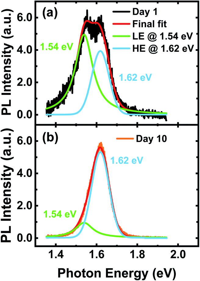 | ||
| Fig. 7 Energy-scaled time-resolved PL spectra integrated in a time delay between 100 and 600 ns after excitation for a perovskite thin film with the composition Cs0.1(FA0.83MA0.17)0.9Pb(I0.83Br0.17)3 deposited on bare glass. The data are collected on (a) the day of sample preparation (day 1) and (b) after storage (day 10). A two-peak pseudo-Voigt profile is used to fit the data for the lower-energy (LE) and higher energy (HE) peaks. | ||
In summary, we identify additional lower-energy states, next to the bulk bandgap, which disappear along with the spontaneous enhancement of the stable power output after a storage period of days. These states can be attributed to either trap states or a low volumetric ratio of a lower-energy phase. Both scenarios could well explain the reduction in trap-assisted non-radiative recombination and consequently the reduced ideality factor of the corresponding PSCs. In order to assess whether a reduction of the trap density is responsible for the spontaneous enhancement in the stable power output, we use the TSC technique which has been previously applied in organic-inorganic perovskite materials for probing the density of electronic trap states.22,51–53
2.7. Suppressed “trap states” in stored perovskite solar cells
Applying the TSC method in complete devices, we investigate changes in the possible trap states for pristine and stored PSCs. Fig. 8a shows the TSC spectra over a temperature range of 25 K to 270 K for a PSC measured on day 1 right after device fabrication as well as day 5 and day 12 after storage when the respective PSC demonstrates spontaneous enhancement in the stable power output. On day 1, we observe two distinct TSC signals at around 88 K and 215 K (denoted as P1 and P2, respectively) and a broad TSC signal at around 245 K (denoted as P3), indicating a broad distribution of trap states in the pristine device. Repeating the same measurement on day 5 and 12 reveals that P1 is not altered, P2 is negligibly reduced compared to day 1, while P3 completely disappears. To be noted is that we assign the first two signals (P1 and P2) to the transport layers, since we observe them for other PSCs with different perovskite absorber layers and the same sequence of transport layers. The current reduction associated to signal P3 is indicative of an overall suppression in trap density over time. Applying the initial rise method, we estimate the activation energy of the trap states corresponding to the P3 signal using the equation| ITSC ∝ exp(−EA/kBT) | (2) |
 | ||
| Fig. 8 (a) Thermally stimulated current (TSC) curves of a Cs0.1(FA0.83MA0.17)0.9Pb(I0.83Br0.17)3 solar cell measured directly after device preparation (day 1) and after storage (day 5 and 12). (b) Arrhenius plot of the respective TSC spectrum measured on day 1. The red line represents the data range used for fitting the initial rise associated to signal P3. | ||
In summary, our TSC results support the explanation of a reduced number of traps within the bulk or at the grain boundaries of the perovskite layer over a storage time period of a few days. However, the trap energy is not directly consistent with the red-shifted luminescence band in the PL results discussed in the previous section. This might be explained by the fact that TSC reveals the position of the trap state with respect to the transport energy Et while the PL might also arise from states slightly below Et. Furthermore, excitonic effects and self-absorption of the PL signal contribute to this difference.55
2.8. Morphology and crystallinity of perovskite thin films
In previous publications, the spontaneous enhancement of the PCE of PSCs has been assigned to small perovskite crystallites merging spontaneously into larger ones in perovskite thin films.15,17 Coalescence leads to a reduction in the number of grain boundaries and the associated trap states, resulting in a reduction in non-radiative recombination and consequently an increased PCE. In order to corroborate the observed coalescence and to obtain information about the surface of the thin film, we employ a series of tapping-mode atomic force microscopy (AFM) analyses on a sample on the day of sample preparation and some days after storage in the dark and in an inert atmosphere. To obtain reliable information about the surface morphology of the perovskite thin films and to prevent electron-beam-induced changes on the film, we avoid using scanning electron microscopy. In order to find the exact same spot on different days of measurements, we first perform an indentation on the surface of the perovskite thin film using a diamond AFM tip (see Fig. S11†). By approaching the indented spot in a range of micrometers, we are able to collect the scans from the exact same spot of the perovskite thin film on different days. In all cases and for several measurements of different samples, the topography of the grains does not change (see Fig. S12†), indicating that there is no reduction at perovskite grain boundaries on the surface of the perovskite thin film over time.Our observation for devices stored in N2 is in accordance with another study in which the spontaneous enhancement has been examined under both ambient and inert conditions and no evidence of coalescence was observed over 2 weeks.18 These results are in agreement with a study by Sheng et al. who investigated the interaction of perovskite thin films with air and N2 at room temperature in the dark.56 They tracked the morphology of perovskite thin films over a timescale of two weeks and demonstrated that perovskite grains grow spontaneously into larger grains in the presence of moisture and oxygen at room temperature. However, their results from SEM and XRD did not show any considerable changes in the grain and crystallite sizes of the perovskite thin films of those samples stored in N2 for the same time period. We notice that in those studies reporting the coalescence of perovskite crystallites along with the spontaneous enhancement of the PCE, the samples were stored in the presence of oxygen, whereas we store the samples in a N2-filled glovebox during the entire storage time and between the measurements.
To provide a more solid judgment whether coalescence occurs in our perovskite thin films during the storage time, we perform XRD measurements over time on Cs0.1FM0.9 perovskite thin films coated on ITO/np-SnO2. XRD results collected on day 1 for the pristine perovskite thin film are shown in Fig. 9. All X-ray reflections are indexed in the cubic space group Pm![[3 with combining macron]](https://www.rsc.org/images/entities/char_0033_0304.gif) m (no. 221), which is in good agreement with the reported literature.57 First, we calculate the crystallite size of the perovskite using the Scherrer equation.58 For a correct calculation of full-width-at-half-maximum (FWHM) and to determine the crystallite size of the perovskite, we measure the XRD spectrum of silicon as a reference in order to correct the instrumental broadening. We observe a negligible change in the crystallite size after a storage period. Furthermore, we observe that the relative intensities of the reflections for perovskite diffraction patterns collected on different days remain consistent and the width of the reflections, which among other effects is mainly reminiscent of the crystal size, has altered only slightly (compare Fig. S13†). The relevant crystallographic parameters are listed in Table S2.† Moreover, the distribution of crystal sizes calculated from XRD spectra also shows no significant change. Taken together with the AFM results, our analyses show no evidence of spontaneous coalescence of the perovskite crystallites for samples aged in N2, in contradiction to previous reports.15,17 Therefore, we conclude that the observed spontaneous enhancement of the photovoltaic performance of the PSCs may not be attributed to the coalescence of the perovskite crystallites only. However, we observe a prominent shift of the (001) reflection of a pristine Cs0.1FM0.9 perovskite thin film from 2θ = 14.19° on day 1 to larger diffraction angles 2θ = 14.25° and 14.31° on day 5 and 10, respectively (see Fig. 9, inset). All other reflection peaks of the perovskite thin film also experience a shift to higher angles through day 1 to day 10. We use the X-ray reflections of the ITO layer at 2θ = 21.47° and 30.35° as the reference to exclude sample height misalignment.59–61 The same trend in crystallite sizes and peak shift is also observed for the Cs0.1FM0.9 perovskite thin films deposited on ITO/np-TiO2, as shown in Fig. S14.† A recent study has reported a shift to higher angles in the XRD patterns of perovskite thin films after storage, which is indicative of plane shrinkage and means more compact atomic packing attributed to age-induced recrystallization.16
m (no. 221), which is in good agreement with the reported literature.57 First, we calculate the crystallite size of the perovskite using the Scherrer equation.58 For a correct calculation of full-width-at-half-maximum (FWHM) and to determine the crystallite size of the perovskite, we measure the XRD spectrum of silicon as a reference in order to correct the instrumental broadening. We observe a negligible change in the crystallite size after a storage period. Furthermore, we observe that the relative intensities of the reflections for perovskite diffraction patterns collected on different days remain consistent and the width of the reflections, which among other effects is mainly reminiscent of the crystal size, has altered only slightly (compare Fig. S13†). The relevant crystallographic parameters are listed in Table S2.† Moreover, the distribution of crystal sizes calculated from XRD spectra also shows no significant change. Taken together with the AFM results, our analyses show no evidence of spontaneous coalescence of the perovskite crystallites for samples aged in N2, in contradiction to previous reports.15,17 Therefore, we conclude that the observed spontaneous enhancement of the photovoltaic performance of the PSCs may not be attributed to the coalescence of the perovskite crystallites only. However, we observe a prominent shift of the (001) reflection of a pristine Cs0.1FM0.9 perovskite thin film from 2θ = 14.19° on day 1 to larger diffraction angles 2θ = 14.25° and 14.31° on day 5 and 10, respectively (see Fig. 9, inset). All other reflection peaks of the perovskite thin film also experience a shift to higher angles through day 1 to day 10. We use the X-ray reflections of the ITO layer at 2θ = 21.47° and 30.35° as the reference to exclude sample height misalignment.59–61 The same trend in crystallite sizes and peak shift is also observed for the Cs0.1FM0.9 perovskite thin films deposited on ITO/np-TiO2, as shown in Fig. S14.† A recent study has reported a shift to higher angles in the XRD patterns of perovskite thin films after storage, which is indicative of plane shrinkage and means more compact atomic packing attributed to age-induced recrystallization.16
 | ||
| Fig. 9 X-ray diffraction patterns (normalized to the (001) peak) for a perovskite thin film with the composition Cs0.1(FA0.83MA0.17)0.9Pb(I0.83Br0.17)3 deposited on glass/ITO/np-SnO2, collected on the day of sample preparation (day 1) and after storage (day 5 and 10). Inset: shift of the (001) perovskite peak from 2θ = 14.16° on day 1 to larger diffraction angles 2θ = 14.23° on day 5 and 2θ = 14.30° on day 10. | ||
A shift in the diffraction peaks demonstrates a change in the d-spacings. Macroscopic strains change the inter-planar spacing by Δdhkl, resulting in a shift in the average position of the diffraction peak of Δθ, while microscopic strain manifests itself in a distribution of the d-spacings Δdhkl which broaden the peak by δθ.62 Here, the observed shift in the diffraction peaks is indicative of macroscopic strain effects. A shift to higher diffraction angles corresponds to smaller d-spacing, and therefore, the initial strain in the crystal lattice is compressive. We hypothesize that along with the spontaneous enhancement of the stable power output, the initial strain in the material is gradually released. This relaxation of the lattice strain results in a shift in the XRD pattern from day 1 to day 5 and 10. Using the mean d-spacing values of the (001) and (002) reflections calculated for different days, we estimate the relative strain, εr = Δd/d, to be equal to 0.73% on day 1 and 0.39% on day 5, compared to day 10 (details are provided in the ESI† for the relevant parameters).63
According to the literature, lattice strain generally exists in the organic-inorganic perovskite films with different compositions and perovskite films are strained even on those substrates which are generally used for high-efficiency PSCs, such as SnO2- or TiO2-covered ITO glass substrates.63 We prepare the perovskite thin films with an antisolvent-assisted film formation method followed by an annealing step (100 °C). This causes the perovskite thin films to nucleate and crystallize very quickly, providing possible mechanisms for defect formation and leaving strain in the perovskite thin film. Our notion is consistent with the suggestions of recent studies examining residual strain in perovskite thin films. These studies demonstrated that strain arises during film growth and crystallization and is associated with the thermal gradient during film processing and a mismatched thermal expansion between perovskite thin films and the substrates on which perovskite films are prepared.63,64 Since the strain level is expected to depend on the substrate (ETL) and inhomogeneous composition in the perovskite films, we also expect a different degree of spontaneous enhancement in stable power output for the various types of PSCs discussed in Section 2.1–2.3.
In several previous studies, lattice strain was inferred to induce defect concentrations and shallow traps that bring about non-radiative recombination.65,66 Using time-resolved PL, Jones et al. revealed that a reduction in lattice strain leads to a reduction in defects that are associated with local non-radiative decay.65 Considering these findings together with our observations, we hypothesize that a reduction in lattice strain over time correlates with reduced shallow trap densities, which is a possible reason for the spontaneous enhancement in the photovoltaic performance of multi-cation-halide PSCs. Our TSC results support the hypothesis of lattice-strain-induced trap states in pristine PSCs and their disappearance over time. Moreover, disappearance of the observed lower-energy states in time-resolved PL measurement after storage can be explained by strain relaxation over time, leading to lower densities of the lower-energy states (e.g. shallow trap states). However, there is no straightforward analysis or method that provides us with direct proof that strain is the origin of the lower-energy states detected by time-resolved PL. Overall, given the generality and magnitude of the spontaneous enhancement for different ETLs and compositions of multi-cation-halide PSCs, we suggest that the spontaneous enhancement needs to be clarified by further studies. Strategies for more quickly inducing morphological changes in order to accelerate the “spontaneous enhancement” might be of significant interest in such a context. In any case, realizing significant absolute PCE increase that the spontaneous enhancement yields is and will be important for developing high-efficiency PSCs.
3. Conclusion
In this study, we show that the spontaneous enhancement of the stable power output is a general phenomenon in multi-cation-halide PSCs. Our study reveals that the spontaneous enhancement is not restricted to specific charge transport layers, as it occurs for three different ETLs, and is independent of the presence of doped spiro-MeOTAD and Au during the storage time. The effect also occurs for various multi-cation-halide perovskite compositions. However, the degree of enhancement differs for different structures with various ETLs and compositions. In general, devices with initially high PCEs tend not to enhance further over time. The highest PCE we observe in this study is an enhanced stable PCE of ∼19% (PCE of 19.6%) after 50 days for a champion triple cation PSC with a np-SnO2 ETL. The PCE is primarily enhanced by an increasing VOC, which is in agreement with a significant increase in the PL intensity and charge carrier lifetime of the perovskite thin films, indicating reduced non-radiative recombination losses. These observations are correlated with a shift in the ideality factor towards bulk carrier recombination. At the same time, time-resolved PL spectra reveal the disappearance of the initially present low-energy states which dominate the emission immediately after film formation. Moreover, structural characterization by AFM and XRD reveals no evidence of significant changes in grain size, but the XRD analysis shows a reduction in lattice strain in the perovskite thin films. TSC characterization discloses the existence of trap states in the pristine PSC fading over time possibly due to strain-induced traps. Taken together with the photophysical data, we suggest that the spontaneous enhancement could originate from the reduction of strain in the perovskite thin films and concomitantly from the disappearance of trap states slightly below the bandgap.4. Experimental section
4.1. Precursor solution preparation
For the ETL, we synthesized TiO2 nanoparticles (np-TiO2) according to an existing recipe.67 We prepared a np-SnO2 solution by diluting 15% aqueous colloids of SnO2 nanoparticles (np-SnO2) (Alfa Aesar) with distilled water to a concentration of 2.04%. We acquired buckminsterfullerene (C60) by dissolving 10 mg ml−1 of C60 (Sigma Aldrich) in 1,2-dichlorobenzene (DCB).For the triple cation perovskite solution, first we prepared a double cation precursor solution by dissolving 1 M formamidinium iodide (FAI, Dyesol), 0.2 M methylammonium bromide (MABr, Dyesol), 0.2 M lead bromide (PbBr2, TCI), and 1.1 M lead iodide (PbI2, TCI) in a 4![[thin space (1/6-em)]](https://www.rsc.org/images/entities/char_2009.gif) :1 (v/v) mixture of dimethylformamide (DMF, Sigma Aldrich) and dimethyl sulfoxide (DMSO, Sigma Aldrich). The resulting perovskite has the stoichiometric formula FA0.83MA0.17Pb(I0.83Br0.17)3. By adding 42.1 μl, 88.9 μl, and 141.2 μl of a 1.5 M cesium iodide (CsI, Alpha Aesar) stock solution in DMSO to 1 ml of the double cation perovskite solution, we acquired the final triple cation perovskite solution of Csx(FA0.83MA0.17)(1−x)Pb(I0.83Br0.17)3 with x = 0.05, 0.1, and 0.15, respectively.
:1 (v/v) mixture of dimethylformamide (DMF, Sigma Aldrich) and dimethyl sulfoxide (DMSO, Sigma Aldrich). The resulting perovskite has the stoichiometric formula FA0.83MA0.17Pb(I0.83Br0.17)3. By adding 42.1 μl, 88.9 μl, and 141.2 μl of a 1.5 M cesium iodide (CsI, Alpha Aesar) stock solution in DMSO to 1 ml of the double cation perovskite solution, we acquired the final triple cation perovskite solution of Csx(FA0.83MA0.17)(1−x)Pb(I0.83Br0.17)3 with x = 0.05, 0.1, and 0.15, respectively.
We prepared the wide bandgap triple cation perovskite solution with the stoichiometric formula Cs0.1(FA0.83MA0.17)0.9Pb(I0.67Br0.33)3 by mixing FAPbI2Br, MAPbI2Br, and CsPbI2Br with a ratio of 0.75%, 15% and 10%, respectively. We diluted FAPbI2Br (0.87 M FAI, 0.43 M FABr, 0.957 M PbI2, and 0.43 M PbBr2) and MAPbI2Br (0.87 M MAI, 0.43 MABr, 0.957 M PbI2, and 0.43 M PbBr2) in a 4:1 (v/v) mixture of DMF:DMSO, while CsPbI2Br (0.87 M CsI, 0.43 M CsBr, 0.957 M PbI2, and 0.43 M PbBr2) was diluted in pure DMSO.
We prepared the double cation perovskite solution with the stoichiometric formula Cs0.17FA0.83(I0.83Br0.17)3 by dissolving 0.83 M FAI, 0.17 M CsI, 1.49 M PbI2, and 0.51 M PbBr2 in a 4:1 (v/v) mixture of DMF:DMSO.
For the HTL, we used a precursor solution containing 80 mg spiro-MeOTAD (Luminescence Technology) dissolved in chlorobenzene (CB) with the additives 4-tert-butylpyridine (4-tBP) (28.5 μl/1 ml CB) and lithium bis(trifluoromethanesulfonyl)imide (Li-TFSI) (17.5 μl/1 ml CB from a 520 mg ml−1 acetonitrile stock solution).
4.2. Solar cell fabrication
Initially, we cleaned the pre-structured 16 × 16 mm2 glass substrates with a 120 nm thick indium tin oxide layer (ITO, sheet resistance 15 Ω, Luminescence Technology) in an ultrasonic bath with acetone and isopropanol for 10 min each. Then we used oxygen plasma at 100 W power for 6 min before deposition of np-TiO2 ETLs and 3 min in the case of using np-SnO2 ETLs.Next, we spin-coated the np-TiO2 ETL at a speed of 7000 rpm for 30 s followed by a 100 °C annealing step for 30 min in an ambient atmosphere. We set the above parameters to 4000 rpm and 200 °C, in the case of using np-SnO2 as the ETL. Moreover, to improve the wettability of np-SnO2 ETLs, we used oxygen plasma treatment shortly before deposition of the perovskite thin film. We processed C60 layers by spin coating the solution at a rate of 1500 rpm for 1 min and annealed the substrates to 75 °C for 2 min, subsequently.
For all compositions of the perovskite thin films, we spin-coated the solution by a two-step process on top of the ETL: (1) 1000 rpm for 10 s and (2) 6000 rpm for 20 s. We poured100 μl of CB on the spinning substrate 10 s prior to the end of the second step. We annealed the samples at 100 °C for 60 min in an inert atmosphere. We deposited the spiro-MeOTAD HTL using a spin-coating process (4000 rpm for 30 s) after 2 min of cooling down to room temperature, followed by overnight oxygen doping in a drybox with a relative humidity of less than 30%. Subsequently, using a Vactec Coat 360 evaporator, we evaporated a 70 nm thick gold (Au) layer through shadow masks on the spiro-MeOTAD layer to complete the fabrication of the perovskite solar cells with an active area of 10.5 mm2. We processed all the layers in an inert atmosphere in a N2-filled glovebox, except for np-TiO2 and np-SnO2 ETLs which we spin-coated under controlled cleanroom conditions: ambient air with a relative humidity of around 45% at room temperature. Fig. S15† shows a cross section SEM image for the glass/ITO/np-SnO2/Cs0.1FM0.9/spiro-MeOTAD/Au configuration.
4.3. Solar cell storage conditions
We stored all the as-fabricated PSCs and perovskite thin films under an inert atmosphere (N2-filled glovebox, room temperature, dry) to maintain identical environmental conditions and in dark boxes to prevent light-induced effects over the storage period.4.4. Characterization
Conflicts of interest
There are no conflicts to declare.Acknowledgements
The authors are grateful to the great spirit of the Taskforce Perovskite Photovoltaics at KIT and the scientific discussions. The authors thank Richard Thelen (KIT), Raphael Schmager (KIT), and Simon Geisert (KIT) for AFM measurements. Somayeh Moghadamzadeh would like to acknowledge the financial support from DAAD (Deutscher Akademischer Austauschdienst/German academic exchange service) for her doctoral research work under personal reference number 91621525. The financial support by the German Federal Ministry of Education and Research (BMBF) through the projects PRINTPERO (03SF0557A), the Initiating and Networking funding of the Helmholtz Association (HYIG of U. W. P. (VH-NG-1148), Recruitment Initiative of B. S. R., the Helmholtz Energy Materials Foundry (HEMF), PEROSEED (ZT-0024), the Science and Technology of Nanostructures (STN), and the Karlsruhe School of Optics & Photonics (KSOP) is gratefully acknowledged.References
- NREL, Perovskite Efficiency Chart, https://www.nrel.gov/pv/assets/pdfs/best-research-cell-efficiencies.20190923.pdf, accessed 23 September 2019 Search PubMed.
- T. Abzieher, S. Moghadamzadeh, F. Schackmar, H. Eggers, F. Sutterlüti, A. Farooq, D. Kojda, K. Habicht, R. Schmager, A. Mertens, R. Azmi, L. Klohr, J. A. Schwenzer, M. Hetterich, U. Lemmer, B. S. Richards, M. Powalla and U. W. Paetzold, Adv. Energy Mater., 2019, 1802995, 1–13 Search PubMed.
- L. Cojocaru, K. Wienands, T. W. Kim, S. Uchida, A. J. Bett, S. Rafizadeh, J. C. Goldschmidt and S. W. Glunz, ACS Appl. Mater. Interfaces, 2018, 10, 26293–26302 CrossRef CAS.
- I. A. Howard, T. Abzieher, I. M. Hossain, H. Eggers, F. Schackmar, S. Ternes, B. S. Richards, U. Lemmer and U. W. Paetzold, Adv. Mater., 2019, 31, 1806702 CrossRef.
- Y. Cho, A. M. Soufiani, J. S. Yun, J. Kim, D. S. Lee, J. Seidel, X. Deng, M. A. Green, S. Huang and A. W. Y. Ho-Baillie, Adv. Energy Mater., 2018, 8, 1–10 Search PubMed.
- E. A. Alharbi, A. Y. Alyamani, D. J. Kubicki, A. R. Uhl, B. J. Walder, A. Q. Alanazi, J. Luo, A. Burgos-Caminal, A. Albadri, H. Albrithen, M. H. Alotaibi, J.-E. Moser, S. M. Zakeeruddin, F. Giordano, L. Emsley and M. Graetzel, Nat. Commun., 2019, 10, 3008 CrossRef PubMed.
- S. Gharibzadeh, B. Abdollahi Nejand, M. Jakoby, T. Abzieher, D. Hauschild, S. Moghadamzadeh, J. A. Schwenzer, P. Brenner, R. Schmager, A. A. Haghighirad, L. Weinhardt, U. Lemmer, B. S. Richards, I. A. Howard and U. W. Paetzold, Adv. Energy Mater., 2019, 9, 1–10 Search PubMed.
- J. A. Schwenzer, L. Rakocevic, R. Gehlhaar, T. Abzieher, S. Gharibzadeh, S. Moghadamzadeh, A. Quintilla, B. S. Richards, U. Lemmer and U. W. Paetzold, ACS Appl. Mater. Interfaces, 2018, 10, 16390–16399 CrossRef CAS.
- C. Zhao, B. Chen, X. Qiao, L. Luan, K. Lu and B. Hu, Adv. Energy Mater., 2015, 5, 1–6 Search PubMed.
- W. Nie, J. C. Blancon, A. J. Neukirch, K. Appavoo, H. Tsai, M. Chhowalla, M. A. Alam, M. Y. Sfeir, C. Katan, J. Even, S. Tretiak, J. J. Crochet, G. Gupta and A. D. Mohite, Nat. Commun., 2016, 7, 1–9 Search PubMed.
- E. T. Hoke, D. J. Slotcavage, E. R. Dohner, A. R. Bowring, H. I. Karunadasa and M. D. McGehee, Chem. Sci., 2015, 6, 613–617 RSC.
- D. W. DeQuilettes, W. Zhang, V. M. Burlakov, D. J. Graham, T. Leijtens, A. Osherov, V. Bulović, H. J. Snaith, D. S. Ginger and S. D. Stranks, Nat. Commun., 2016, 7, 11683 CrossRef CAS.
- A. Gomez, Q. Wang, A. R. Goni, M. Campoy-Quiles and A. Abate, Energy Environ. Sci., 2019, 12, 2537–2547 RSC.
- R. Inoue, S. Ishikawa, R. Imura, Y. Kitanaka, T. Oguchi, Y. Noguchi and M. Miyayama, Sci. Rep., 2015, 5, 14741 CrossRef CAS PubMed.
- B. Roose, A. Ummadisingu, J. P. Correa-Baena, M. Saliba, A. Hagfeldt, M. Graetzel, U. Steiner and A. Abate, Nano Energy, 2017, 39, 24–29 CrossRef CAS.
- C. Fei and H. Wang, Org. Electron., 2019, 68, 143–150 CrossRef CAS.
- T. T. Ngo, E. M. Barea, R. Tena-Zaera and I. Mora-Seró, ACS Appl. Energy Mater., 2018, 1, 4057–4064 CrossRef CAS.
- C. Bi, X. Zheng, B. Chen, H. Wei and J. Huang, ACS Energy Lett., 2017, 2, 1400–1406 CrossRef CAS.
- N. Ito, M. A. Kamarudin, D. Hirotani, Y. Zhang, Q. Shen, Y. Ogomi, S. Iikubo, T. Minemoto, K. Yoshino and S. Hayase, J. Phys. Chem. Lett., 2018, 9, 1682–1688 CrossRef CAS PubMed.
- A. K. Jena and T. Miyasaka, in Organic-Inorganic Halide Perovskite Photovoltaics: from Fundamentals to Device Architectures, ed. N.-G. Park, M. Graetzel and T. Miyasaka, Springer International Publishing, Switzerland 2016, pp. 255–284 Search PubMed.
- M. Saliba, T. Matsui, J.-Y. Seo, K. Domanski, J.-P. Correa-Baena, M. K. Nazeeruddin, S. M. Zakeeruddin, W. Tress, A. Abate, A. Hagfeldt and M. Graetzel, Energy Environ. Sci., 2016, 9, 1989–1997 RSC.
- Y. Hu, E. M. Hutter, P. Rieder, I. Grill, J. Hanisch, M. F. Aygüler, A. G. Hufnagel, M. Handloser, T. Bein, A. Hartschuh, K. Tvingstedt, V. Dyakonov, A. Baumann, T. J. Savenije, M. L. Petrus and P. Docampo, Adv. Energy Mater., 2018, 1703057, 1–11 Search PubMed.
- E. Climent-Pascual, B. C. Hames, J. S. Moreno-Ramírez, A. L. Álvarez, E. J. Juarez-Perez, E. Mas-Marza, I. Mora-Seró, A. De Andrés and C. Coya, J. Mater. Chem. A, 2016, 4, 18153–18163 RSC.
- M. De Bastiani, V. D'Innocenzo, S. D. Stranks, H. J. Snaith and A. Petrozza, APL Mater., 2014, 2, 081509 CrossRef.
- E. M. Miller, Y. Zhao, C. C. Mercado, S. K. Saha, J. M. Luther, K. Zhu, V. Stevanović, C. L. Perkins and J. Van De Lagemaat, Phys. Chem. Chem. Phys., 2014, 16, 22122–22130 RSC.
- A. N. Cho and N. G. Park, ChemSusChem, 2017, 10, 3687–3704 CrossRef CAS PubMed.
- K. Wojciechowski, S. D. Stranks, A. Abate, G. Sadoughi, A. Sadhanala, N. Kopidakis, G. Rumbles, C. Z. Li, R. H. Friend, A. K. Y. Jen and H. J. Snaith, ACS Nano, 2014, 8, 12701–12709 CrossRef CAS PubMed.
- F. Cai, L. Yang, Y. Yan, J. Zhang, F. Qin, D. Liu, Y. B. Cheng, Y. Zhou and T. Wang, J. Mater. Chem. A, 2017, 5, 9402–9411 RSC.
- Y. Li, Y. Zhao, Q. Chen, Y. Yang, Y. Liu, Z. Hong, Z. Liu, Y. T. Hsieh, L. Meng, Y. Li and Y. Yang, J. Am. Chem. Soc., 2015, 137, 15540–15547 CrossRef CAS PubMed.
- Q. Jiang, X. Zhang and J. You, Small, 2018, 1801154, 1–14 Search PubMed.
- A. Farooq, I. M. Hossain, S. Moghadamzadeh, J. A. Schwenzer, T. Abzieher, B. S. Richards, E. Klampaftis and U. W. Paetzold, ACS Appl. Mater. Interfaces, 2018, 10, 21985–21990 CrossRef CAS PubMed.
- Q. Jiang, L. Zhang, H. Wang, X. Yang, J. Meng, H. Liu, Z. Yin, J. Wu, X. Zhang and J. You, Nat. Energy, 2016, 2, 16177 CrossRef.
- T. Singh and T. Miyasaka, Adv. Energy Mater., 2018, 8, 1–9 Search PubMed.
- T. Leijtens, G. E. Eperon, S. Pathak, A. Abate, M. M. Lee and H. J. Snaith, Nat. Commun., 2013, 4, 1–8 Search PubMed.
- G. Xing, B. Wu, S. Chen, J. Chua, N. Yantara, S. Mhaisalkar, N. Mathews and T. C. Sum, Small, 2015, 11, 3606–3613 CrossRef CAS PubMed.
- H. Li, C. Li, S. Wen, C. Wang, G. Wang, C. Li, C. Wang, L. Huang, W. Dong and S. Ruan, ACS Sustainable Chem. Eng., 2018, 6, 11295–11302 CrossRef CAS.
- Y. Lee, S. Paek, K. T. Cho, E. Oveisi, P. Gao, S. Lee, J. S. Park, Y. Zhang, R. Humphry-Baker, A. M. Asiri and M. K. Nazeeruddin, J. Mater. Chem. A, 2017, 5, 12729–12734 RSC.
- Y. Lee, S. Lee, G. Seo, S. Paek, K. T. Cho, A. J. Huckaba, M. Calizzi, D. won Choi, J. S. Park, D. Lee, H. J. Lee, A. M. Asiri and M. K. Nazeeruddin, Adv. Sci., 2018, 5, 1–6 Search PubMed.
- Y. H. Lee, J. Luo, M.-K. Son, P. Gao, K. T. Cho, J. Seo, S. M. Zakeeruddin, M. Graetzel and M. K. Nazeeruddin, Adv. Mater., 2016, 28, 3966–3972 CrossRef CAS PubMed.
- D. Yang, X. Zhou, R. Yang, Z. Yang, W. Yu, X. Wang, C. Li, S. Liu and R. P. H. Chang, Energy Environ. Sci., 2016, 9, 3071–3078 RSC.
- Z. Li, C. Xiao, Y. Yang, S. P. Harvey, D. H. Kim, J. A. Christians, M. Yang, P. Schulz, S. U. Nanayakkara, C. S. Jiang, J. M. Luther, J. J. Berry, M. C. Beard, M. M. Al-Jassim and K. Zhu, Energy Environ. Sci., 2017, 10, 1234–1242 RSC.
- J. P. Bastos, U. W. Paetzold, R. Gehlhaar, W. Qiu, D. Cheyns, S. Surana, V. Spampinato, T. Aernouts and J. Poortmans, Adv. Energy Mater., 2018, 8, 1–9 Search PubMed.
- J. Chen and N. G. Park, Adv. Mater., 2018, 1803019, 1–56 Search PubMed.
- W. E. I. Sha, H. Zhang, Z. S. Wang, H. L. Zhu, X. Ren, F. Lin, A. K. Jen and W. C. H. Choy, Energy Environ. Sci., 2018, 1701586, 1–7 Search PubMed.
- G. J. A. H. Wetzelaer, M. Scheepers, A. M. Sempere, C. Momblona, J. Ávila and H. J. Bolink, Adv. Mater., 2015, 27, 1837–1841 CrossRef CAS PubMed.
- J. P. Correa-Baena, W. Tress, K. Domanski, E. H. Anaraki, S. H. Turren-Cruz, B. Roose, P. P. Boix, M. Graetzel, M. Saliba, A. Abate and A. Hagfeldt, Energy Environ. Sci., 2017, 10, 1207–1212 RSC.
- P. Calado, D. Burkitt, J. Yao, J. Troughton, T. M. Watson, M. J. Carnie, A. M. Telford, B. C. O'Regan, J. Nelson and P. R. F. Barnes, Phys. Rev. Appl., 2019, 11, 1 Search PubMed.
- J. P. Correa-Baena, S. H. Turren-Cruz, W. Tress, A. Hagfeldt, C. Aranda, L. Shooshtari, J. Bisquert and A. Guerrero, ACS Energy Lett., 2017, 2, 681–688 CrossRef CAS.
- W. Tress, M. Yavari, K. Domanski, P. Yadav, B. Niesen, J. P. Correa Baena, A. Hagfeldt and M. Graetzel, Energy Environ. Sci., 2018, 11, 151–165 RSC.
- J. Mooney and P. Kambhampati, J. Phys. Chem. Lett., 2013, 4, 3316–3318 CrossRef CAS.
- R. R. Haering and E. N. Adams, Phys. Rev., 1960, 117, 451–454 CrossRef CAS.
- K. Kawano and C. H. Adachi, Adv. Funct. Mater., 2009, 19, 3934–3940 CrossRef CAS.
- A. Baumann, S. Väth, P. Rieder, M. C. Heiber, K. Tvingstedt and V. Dyakonov, J. Phys. Chem. Lett., 2015, 6, 2350–2354 CrossRef CAS PubMed.
- A. Kadashchuk, R. Schmechel, H. Von Seggern, U. Scherf and A. Vakhnin, J. Appl. Phys., 2005, 98, 024101 CrossRef.
- A. Bercegol, D. Ory, D. Suchet, S. Cacovich, O. Fournier, J. Rousset and L. Lombez, Nat. Commun., 2019, 10, 1586 CrossRef PubMed.
- R. Sheng, X. Wen, S. Huang, X. Hao, S. Chen, Y. Jiang, X. Deng, M. A. Green and A. W. Y. Ho-Baillie, Nanoscale, 2016, 8, 1926–1931 RSC.
- T. J. Jacobsson, L. J. Schwan, M. Ottosson, A. Hagfeldt and T. Edvinsson, Inorg. Chem., 2015, 54, 10678–10685 CrossRef CAS PubMed.
- F. W. Jones, Proc. R. Soc. London, Ser. A, 1938, 166, 16–43 CrossRef CAS.
- M. Thirumoorthi and J. Thomas Joseph Prakash, J. Asian Ceram. Soc., 2016, 4, 124–132 CrossRef.
- S. Y. Ryu, J. H. Seo, H. Hafeez, M. Song, J. Y. Shin, D. H. Kim, Y. C. Jung and C. S. Kim, J. Phys. Chem. C, 2017, 121, 9191–9201 CrossRef CAS.
- Y. Jouane, S. Colis, G. Schmerber, P. Kern, A. Dinia, T. Heiser and Y. A. Chapuis, J. Mater. Chem., 2011, 21, 1953–1958 RSC.
- R. E. Dinnebier and S. J. L. Billinge, in Powder Diffraction: Theory and Practice, ed. R. E. Dinnebier and S. J. L. Billinge, Royal Society of Chemistry (RSC), Cambridge, United Kingdom, 2008, p. 16 Search PubMed.
- J. Zhao, Y. Deng, H. Wei, X. Zheng, Z. Yu, Y. Shao, J. E. Shield and J. Huang, Sci. Adv., 2017, 3, 3–8 Search PubMed.
- C. Zhu, X. Niu, Y. Fu, N. Li, C. Hu, Y. Chen, X. He, G. Na, P. Liu, H. Zai, Y. Ge, Y. Lu, X. Ke, Y. Bai, S. Yang, P. Chen, Y. Li, M. Sui, L. Zhang, H. Zhou and Q. Chen, Nat. Commun., 2019, 10, 815 CrossRef PubMed.
- T. W. Jones, A. Osherov, M. Alsari, M. Sponseller, B. C. Duck, Y. K. Jung, C. Settens, F. Niroui, R. Brenes, C. V. Stan, Y. Li, M. Abdi-Jalebi, N. Tamura, J. E. MacDonald, M. Burghammer, R. H. Friend, V. Bulović, A. Walsh, G. J. Wilson, S. Lilliu and S. D. Stranks, Energy Environ. Sci., 2019, 12, 596–606 RSC.
- J. T. W. Wang, Z. Wang, S. Pathak, W. Zhang, D. W. Dequilettes, F. Wisnivesky-Rocca-Rivarola, J. Huang, P. K. Nayak, J. B. Patel, H. A. Mohd Yusof, Y. Vaynzof, R. Zhu, I. Ramirez, J. Zhang, C. Ducati, C. Grovenor, M. B. Johnston, D. S. Ginger, R. J. Nicholas and H. J. Snaith, Energy Environ. Sci., 2016, 9, 2892–2901 RSC.
- I. M. Hossain, D. Hudry, F. Mathies, T. Abzieher, S. Moghadamzadeh, D. Rueda-Delgado, F. Schackmar, M. Bruns, R. Andriessen, T. Aernouts, F. Di Giacomo, U. Lemmer, B. S. Richards, U. W. Paetzold and A. Hadipour, ACS Appl. Energy Mater., 2019, 2, 47–58 CrossRef CAS.
Footnote |
| † Electronic supplementary information (ESI) available. See DOI: 10.1039/c9ta09584e |
| This journal is © The Royal Society of Chemistry 2020 |