
 Open Access Article
 This Open Access Article is licensed under a
 Creative Commons Attribution 3.0 Unported Licence
Flat band potential determination: avoiding the pitfalls†
Anna
Hankin
 *ac,
Franky E.
Bedoya-Lora‡
a,
John C.
Alexander§
b,
Anna
Regoutz¶
b and
Geoff H.
Kelsall
a
*ac,
Franky E.
Bedoya-Lora‡
a,
John C.
Alexander§
b,
Anna
Regoutz¶
b and
Geoff H.
Kelsall
a
aDepartment of Chemical Engineering, Imperial College London, London, SW7 2AZ, UK. E-mail: anna.hankin@imperial.ac.uk
bDepartment of Materials, Imperial College London, London, SW7 2AZ, UK
cInstitute of Molecular Science and Engineering, Imperial College London, London, UK
First published on 8th November 2019
Abstract
The flat band potential is one of the key characteristics of photoelectrode performance. However, its determination on nanostructured materials is associated with considerable uncertainty. The complexity, applicability and pitfalls associated with the four most common experimental techniques used for evaluating flat band potentials, are illustrated using nanostructured synthetic hematite (α-Fe2O3) in strongly alkaline solutions as a case study. The motivation for this study was the large variance in flat band potential values reported for synthetic hematite electrodes that could not be justified by differences in experimental conditions, or by differences in their charge carrier densities. We demonstrate through theory and experiments that different flat band potential determination methods can yield widely different results, so could mislead the analysis of the photoelectrode performance. We have examined: (a) application of the Mott–Schottky (MS) equation to the interfacial capacitance, determined by electrochemical impedance spectroscopy as a function of electrode potential and potential perturbation frequency; (b) Gärtner–Butler (GB) analysis of the square of the photocurrent as a function of electrode potential; (c) determination of the potential of transition between cathodic and anodic photocurrents during slow potentiodynamic scans under chopped illumination (CI); (d) open circuit electrode potential (OCP) under high irradiance. Methods GB, CI and OCP were explored in absence and presence of H2O2 as hole scavenger. The CI method was found to give reproducible and the most accurate results on hematite but our overall conclusion and recommendation is that multiple methods should be employed for verifying a reported flat band potential.
Introduction
Much global research is being dedicated presently to the development of new materials and new material structures with improved stability and catalytic activity for use in energy conversion systems, such as photoelectrochemical reactors for water splitting. These reactors incorporate semiconducting photoelectrode materials which absorb photons with energies equal to or greater than the band gap, generating electrical charge carriers. The process of solar energy conversion to chemical energy is completed subsequently by the transfer of this photo-generated electrical charge across semiconductor|electrolyte interfaces, provided the photo-generated bias and the alignment of electronic energy levels across those interfaces are favourable.1–4Material modification techniques are being employed in attempts to enhance solar-to-fuel conversion efficiencies. One set of such techniques can be described collectively as ‘nanostructuring’,5–7 a term that broadly encompasses: modifications of bulk material structures to improve charge transport properties,8,9 nanotexturing of surfaces to enhance photon absorption7,10–13 and decoration of surfaces with catalyst particles to improve reaction kinetics via plasmonic effects.14–16 While nanostructuring is proving to be beneficial to the improvement of energy conversion efficiencies, it also complicates the characterization of the fundamental properties of the modified materials.
The flat band potential is one of the key parameters that determines, and is used in the evaluation of, photoelectrode performance. Its determination can also help to estimate the positions of band edges in new materials. We have reported previously17 that for a single material there can be a wide dispersion in flat band potential values in the literature, which cannot be reconciled by differences in experimental conditions employed in their determination. Furthermore, a large proportion of these values were found to be outside the range predicted theoretically. In this study, we sought to establish the extent to which a flat band potential value may be compromised by the method employed for its determination. To do this, we compared the flat band potential values obtained for one material (α-Fe2O3) using four different techniques:
(a) MS – application of the Mott–Schottky equation to the semiconductor capacitance, determined by electrochemical impedance spectroscopy (EIS) as a function of electrode potential and potential perturbation frequency;
(b) GB – Gärtner–Butler analysis of the square of the photocurrent as a function of electrode potential;
(c) CI – determination of the potential of transition between cathodic and anodic photocurrents during a slow potentiodynamic scan under chopped illumination;
(d) OCP – open circuit electrode potential under high irradiance.
To our knowledge, this is the first time that a systematic investigation of multiple flat band potential determination techniques and quantitative comparison of their results for a given material is offered to the community of scientists and engineers working on photoelectrochemical systems. We sought to demonstrate both theoretically and experimentally that the Mott–Schottky method, so frequently employed for the purpose of characterising newly-developed materials, is unlikely to yield definitive flat band potential (or band edge potential) values, even if the Mott–Schottky plots seem to look ‘right’. We offer complete sets of experimental data obtained with each flat band potential determination technique and attempt to elucidate the physical chemistry responsible for the observations, some of which may also offer new insights into the characteristics of the hematite|liquid junction.
Theory
Theoretical constraint to flat band potential
Prior to experimental analysis, when possible, it is helpful to estimate the flat band potential analytically. The first step is to calculate the electron affinity (conduction band energy) of the semiconductor on the physical scale; the second step is to convert this value to the absolute potential scale.17–21 Then, it should be assumed that on the absolute potential scale, the potential of a non-degenerate semiconductor at the flat band condition, UF(FB), is constrained to a position between that corresponding to the conduction band edge, UC(FB), and that of the valence band edge, UV(FB), throughout the depth of the semiconductor as indicated in eqn (1) and shown schematically in Fig. 1.| UC(FB) < UF(FB) < UV(FB) | (1) |
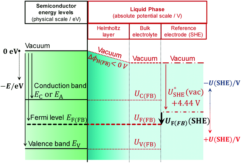 | ||
| Fig. 1 Energy level diagram and corresponding potentials for an arbitrary semiconductor|electrolyte junction at the flat band condition, UF = UF(FB), and when the solution pH is greater than pH of point of zero charge of the electrode, pH > pHpzc, giving rise to a negative potential prop across the Helmholtz layer (ΔϕH(FB) < 0 V). | ||
Hence, any flat band potential value, determined experimentally, should be compared against the condition specified in eqn (1). For hematite, the potential of the conduction band at the flat band potential has been determined theoretically at 298 K as a function of pH:17
 | (2) |
The value of 0.88 (±0.29) was derived using the optical band gap of 2.05 (±0.15) eV and an electron affinity of −4.85 (±0.08) eV. The accuracy of using the optical band gap to estimate the electron affinity22 in an oxide semiconductor is discussed later in the manuscript.
For example, in 1 M NaOH solutions, the measured pH is typically 13.65 (±0.1) and so  is +0.07 (±0.29) V (SHE); hence,
  is predicted to be positive of this value. This prediction will now be compared with experimental findings.
Methods for flat band determination
 | (3) |
Typically, for a semiconductor electrode, CH is assigned values between 0.1 F m−2![[thin space (1/6-em)]](https://www.rsc.org/images/entities/char_2009.gif) 23,24 and 0.2 F m−2.25–27 The semi-conductor capacitance is described by the Mott–Schottky equation, which for an n-type material is:
23,24 and 0.2 F m−2.25–27 The semi-conductor capacitance is described by the Mott–Schottky equation, which for an n-type material is:
 | (4) |
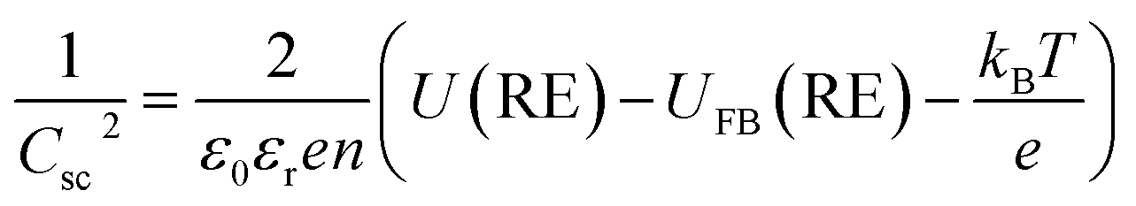
In practice, a Mott–Schottky plot is usually considered to be a graph of 1/CInterface2 as a function of U;3CInterface is determined by EIS measurements. UFB is determined from the intercept of the linear portion of the Mott–Schottky plot with the potential axis, UFB = (U − kBT/e)y=0. Additionally, the charge carrier concentration n may be determined from the gradient of the Mott–Schottky plot, provided the relative permittivity is known.
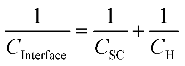
The semiconductor capacitance will vary with the extent of band bending, while the capacitance of the Helmholtz layer is expected to remain constant. Hence, it is often assumed that CH ≫ CSC such that CSC ≈ CInterface.
Another fundamental assumption of the Mott–Schottky eqn (4) is that U − UFB represents exclusively the extent of band bending in the semiconductor, ΔϕSC. However, an applied bias across a semiconductor|solution interface will be distributed between two physical regions: the semiconductor (solid phase) and the Helmholtz layer (liquid phase). Hence, the above assumption is true only if |ΔϕSC| ≫ |ΔϕH|,4,24 where ΔϕH is the potential drop across the Helmholtz layer. However, in general
| U − UFB = ΔϕSC + ΔϕH | (5) |
The justification of the two assumptions above will now be examined theoretically.
The semiconductor capacitance may be estimated by solving the Poisson equation, as shown in Section 1 in the ESI,† for the case of a n-type semiconductor in which the bulk concentrations of electrons, holes and donors are symbolised with e0, po and ND, respectively, yielding eqn (6) for the semiconductor capacitance:
 | (6) |
Hence, the capacitance of the space charge layer may be predicted as a function of the extent of band bending, provided the relative permittivity and bulk charge carrier densities in the semiconductor are known. The dielectric constant of α-Fe2O3 has been reported as 24.1,28 38.2,29 8030 and 120;31 such a wide range results in a significant difference in predicted capacitance values. Nevertheless, the interfacial capacitance may now be estimated from eqn (6).
To illustrate the fact that in practice Mott–Schottky plots may contain non-negligible contributions from the Helmholtz layer capacitance, in Fig. 2 we compare theoretical values of 1/CSC2 with 1/CInterface2 as a function of semiconductor band bending for a typical semiconductor|electrolyte interface. Note that C−2 is plotted on a logarithmic scale to facilitate comparison of data sets. It is evident that an experimentally determined interfacial capacitance should be corrected by the capacitance of the Helmholtz layer in order to obtain meaningful Mott–Schottky plots. This appears to be particularly important for highly doped semiconductors (ND > ca. 1023 m−3). It is also evident that if capacitance is measured over a sufficiently broad range of band bending, then the graphs of 1/CSC2 for different dopant densities converge to one value, from which the value of CH may be estimated, unless prohibited by material instability over the required potential range. An alternative approach to the determination of CH is presented elsewhere.32
 | ||
Fig. 2 Interfacial (![[dash dash, graph caption]](https://www.rsc.org/images/entities/char_e091.gif) ) and semiconductor (–) capacitance as a function of potential drop in an n-type semiconductor with εr = 80, n0 ≈ ND (for various doping levels), p0 ≈ 0 and CH = 0.2 F m−2. ) and semiconductor (–) capacitance as a function of potential drop in an n-type semiconductor with εr = 80, n0 ≈ ND (for various doping levels), p0 ≈ 0 and CH = 0.2 F m−2. | ||
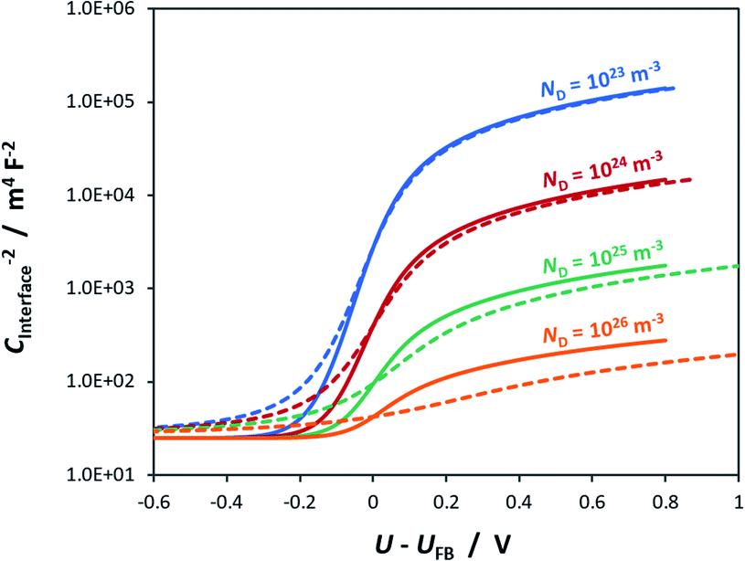
Fig. 3 illustrates the extent to which the Mott–Schottky plot can be affected by CH for a n-type semiconductor with a donor density of 1026 m−3. It is clearly evident that if the Mott–Schottky plot was constructed using CInterface, without correction for CH, the flat band potential values would appear more negative and thus incorrect values would be determined from extrapolation of the curve to the x-axis. Furthermore, it is important to note that, contrary to previous reports,24,32 even after correction by CH, linearity of Mott–Schottky plots is not always guaranteed.
 | ||
| Fig. 3 Simulated Mott–Schottky plots for an n-type semiconductor with εr = 80 and n0 ≈ ND = 1026 m−3 when interfaced with solution for CH: 0.10, 0.15 and 0.20 F m−2. Graphs illustrate the difference between the true semiconductor capacitance (–) and the recorded interfacial () capacitance. | ||
The next problem is the frequent assumption that U − UFB ≈ ΔϕSC (eqn (4)); hence Mott–Schottky graphs in Fig. 2 are often simply plotted versus U, such that UFB can be determined by extrapolation. However, this assumption is not always justifiable.
If CH is known, it is possible to predict the distribution of applied potential between semiconductor and Helmholtz layer, by assuming that the charge in the semiconductor space charge region, qSC, is compensated by free charges, qH, in the Helmholtz layer: qSC = qH.33
As shown in Fig. 4, the proportion of applied bias that is dropped across the Helmholtz layer increases with increasing dopant density, which is expected as the semiconductor will begin to exhibit quasi-metallic behaviour; predictably, for an n-type semiconductor it is also greater in the state of accumulation than in the state of depletion. Hence, unless a semiconductor has very low dopant levels, it cannot be assumed that U − UFB ≈ ΔϕSC; if such an assumption is made erroneously, then the gradient of the Mott–Schottky graph used for computing the doping level (eqn (7)) will be incorrect.
 | (7) |
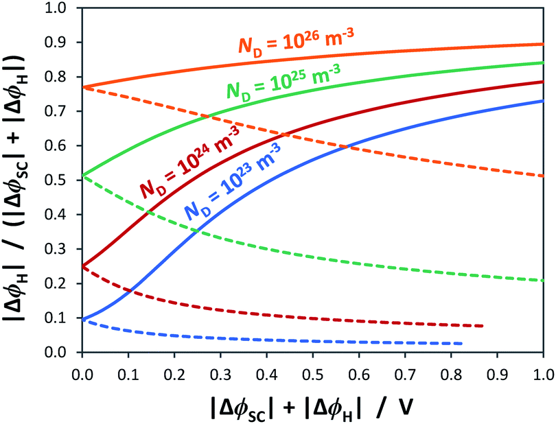 | ||
| Fig. 4 Relative distribution of applied bias between the space charge layer of an n-type semiconductor with εr = 80 and Helmholtz layer with CH = 0.2 F m−2 for the cases of depletion () and accumulation (–). | ||
We note that the change in ΔϕH as a function of applied potential, will also cause the potentials of the conduction and valence band edges to shift.
For example, Fig. 5 shows Mott–Schottky plots for a n-type semiconductor with different doping levels for the cases of U − UFB = ΔϕSC + ΔϕH and U − UFB ≈ ΔϕSC. Clearly, at doping levels >1024 m−3, the gradients of the Mott–Schottky plots are affected severely by the partial distribution of the applied bias across the Helmholtz layer; this must be taken into account in the analysis of interfacial capacitance determined by impedance spectroscopy as a function of U − UFB. If the data is not corrected for ΔϕH, the doping density may be over-estimated.
 | ||
| Fig. 5 Interfacial capacitance as a function of bias applied across the semiconductor|electrolyte interface for an n-type semiconductor with εr = 80, n0 ≈ ND (for various doping levels), p0 ≈ 0 and CH = 0.2 F m−2 for the cases of U − UFB = ΔϕSC + ΔϕH () and U − UFB ≈ ΔϕSC (–). | ||
 | (8) |
In most cases, the semiconductor|electrolyte interface has a finite resistance; Fig. 6 shows the most basic equivalent circuit that is applicable.
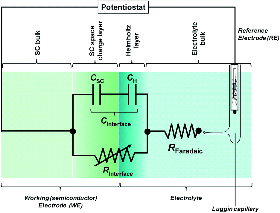 | ||
| Fig. 6 Electronic representation of the semiconductor|electrolyte interface. RInterface is a variable resistor. | ||
The impedance of the electronic circuit shown in Fig. 6 is computed according to:
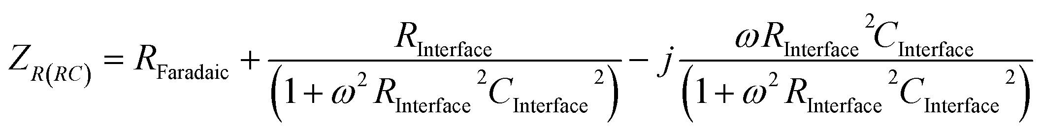 | (9) |
The evaluation of RC parameters may be accomplished by fitting the circuit model to experimental measurements of the semiconductor|electrolyte impedance measured over a wide range of perturbation frequencies (typically 105 to 0.1 Hz), applied to a range of potentials. CInterface, obtained as a function of applied potential, can be corrected subsequently by CH and ΔϕH to obtain CSC as a function of band bending, so allowing the determination of flat band potential and charge carrier density using the Mott–Schottky equation.
Complications arise when multiple processes take place on the semiconductor surface, when the circuit in Fig. 6 becomes too simplistic. It can be challenging to distinguish between processes responsible for the different impedance features, such as several semicircles on a Nyquist plot, especially if they are convoluted. It is often not possible to isolate the required semicircle for analysis, in which case a more complex equivalent circuit is employed to describe the full data set and the relevant parameters are subsequently extracted from the fit. This can require guesswork as to which processes are occurring and whether they are in series or parallel relative to each other, as discussed in Section 3 in the ESI.† Additionally, it is common to replace capacitors, C, in the equivalent circuits with constant phase elements, CPE, to account for non-ideal capacitive behaviour associated with spatial distributions of potential and so to obtain a better agreement between the circuit model and experimental data.34 Conversion of CPE to effective capacitances for complex circuits introduces additional error, as discussed in Section 4 in the ESI.† Moreover, the impedance data collected over a wide potential range often cannot be modelled with the same equivalent circuit; at the same time, it is wise to determine interfacial behaviour across a wide potential range in order to minimise the range over which the graphs need to be extrapolated. Mott–Schottky graphs are often extrapolated by >0.5 V and sometimes even >1 V, yet Fig. 2, 3 and 5 illustrate the likely serious error of doing so from a limited data set.
In summary, when EIS data is processed and a Mott–Schottky plot is generated, there can be considerable uncertainty in the data trend and the extracted values. Indeed Mott–Schottky plots can be totally meaningless. However, as seen from Fig. 3, the very appearance of a Mott–Schottky plot can indicate deviation from ideal behaviour and the model's assumptions listed below. Comparison between expected and determined flat band potential values should increase confidence in reported values. Additionally, when donor densities extracted from the slopes of Mott–Schottky plots appear particularly large (greater than ca. 1025 m−3), they should be compared with the (reasonably) expected density of states in the conduction band (for n-type materials) or valence band (for p-type materials) to ensure that physics is not violated.
The fundamental assumptions made in the derivation of the Mott–Schottky equation were:35
(1) The resistance of the electrolyte and bulk semiconductor are negligible;
(2) The semiconductor|electrolyte barrier has an infinitely high resistance;
(3) There are no interfacial regions, such as the Helmholtz layer, from which additional capacitive contributions will arise;
(4) There are no surface states, from which additional capacitive contributions will arise;
(5) Donor or acceptor atoms are completely ionised;
(6) Constant relative permittivity, εr;
(7) Spatial distribution of dopants/defects is homogeneous;
(8) The semiconductor surface is perfectly smooth.
Furthermore, it is assumed implicitly that band edges of the semiconductor are ‘pinned’, while the Fermi level can shift.
Assumptions 1, 2 and 4 do not necessarily have to hold if an appropriate circuit is chosen with which to model impedance data, accounting for all parameters.
Assumption 3 is not valid for semiconductor|electrolyte interfaces, so requiring correction. As shown in Fig. 2, 3 and 5, the effect of CH on the gradient and intercept of the resultant Mott–Schottky plot depends on the dopant density.
Assumption 5 may not hold if there is more than one type of donor or acceptor; for example, there may be deep and shallow donors which become ionised at different electrode potentials and give rise to a Mott–Schottky plot with two regions over which gradients differ.30 Without prior detailed knowledge of the semiconductor's composition, it will be difficult to distinguish between this situation and one caused by the influence of the Helmholtz capacitance (Fig. 3).
Very often, instead of using circuit fitting to model EIS data and derive resistances and capacitances, Mott–Schottky plots are constructed from EIS data collected at single frequencies; however, this can yield accurate data only for well-behaved materials.36–39 The assumption that EIS measurements at sufficiently high frequencies (1 to 102 kHz)4 exclude the influence of phenomena such as leakage currents and interference of surface states40 needs to be verified experimentally. Furthermore, the frequency dispersion in the gradients of Mott–Schottky plots has been explained by a semiconductor's violation of assumption 6.38,41 This has been thought to compromise the determination of the dopant density but not the flat band potential value, provided the graphs generated at multiple frequencies converge to the same potential value. However, as stated earlier, if data has to be extrapolated over a wide potential range, there can be little confidence that curves do indeed converge to one value.
Spatial distribution of dopants42 or non-stoichiometric ions43 through the thickness of the semiconductors, which can be caused readily by thermal pre-treatment,44 for example, results in a conductivity profile and non-linearity in Mott–Schottky plots.38 Hematite is especially known for having an inhomogeneous composition near the surface,38 violating assumption 7.
Assumption 8 is violated by nanostructured materials. Their real surface area is substantially larger than their geometric surface area, compromising the calculation of capacitance per unit area required for eqn (4), leading to an apparently more negative flat band potential in the case of a n-type semiconductor.
A further complication arises when the dimensions of the nanofeatures, such as nanowires or dendrites, are comparable with, or greater than, the width of the semiconductor space charge layer.45 If the width of the space charge layer exceeds the size of nanofeatures at the surface, then these features will be fully depleted. Therefore, as band bending increases, the area over which the capacitance changes is decreased from the real surface area towards the geometric surface area; hence the area becomes a potential-dependent parameter. This manifests as a curved Mott–Schottky plot45 and advanced modelling and accurate knowledge of material and material|electrolyte interfacial properties (εr, ND, CH, presence or otherwise of surface states etc.) is required to achieve meaningful analysis of such plots.
In summary, the semiconductors being synthesized today for direct water splitting will tend to violate most of the assumptions behind the derivation of the Mott–Schottky equation, which nevertheless continues to be used for flat band potential determination, yielding an unhelpfully broad range of values for similar materials.
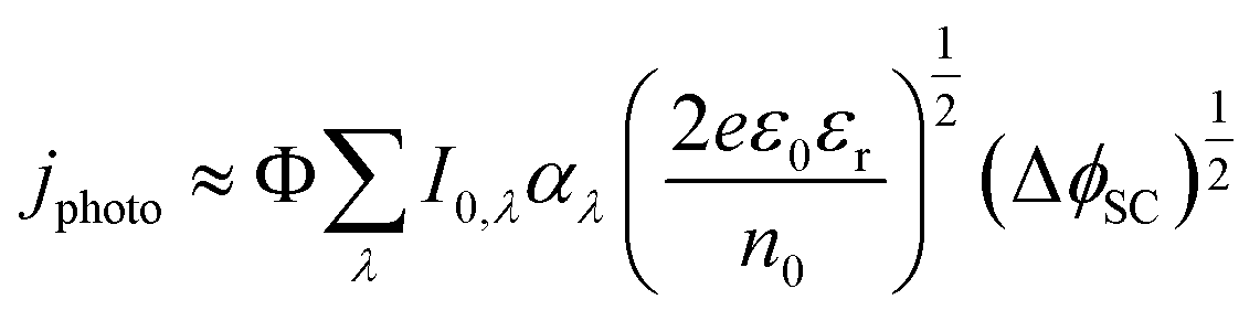
The Gärtner–Butler equation relates the net measured photocurrent, jphoto, to the extent of band bending in the semiconductor, ΔϕSC, via:
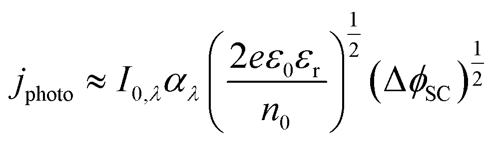 | (10) |
Eqn (10) is a simplified composite of several formulations. In the first, the total photocurrent density46 depends on the incident photon flux, I0,λ (monochromatic), material absorption coefficient, αλ (wavelength-dependent), diffusion length of minority charge carriers, bulk concentration of minority charge carriers and the width of the space charge layer, dSC. The second is a derivation of dSC, which is based on the same assumptions as the Mott–Schottky equation. The simplification of the combined equation is made by assuming that diffusion of minority charge carriers and absorption of photons outside the space charge layer make negligible contributions to the overall current in wide band gap semiconductors,47 as shown in Section 2 in the ESI,† and that only photon absorption in the space charge layer generates photocurrent.
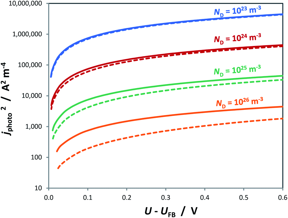
Similar to the manner in which the Mott–Schottky equation is being applied, the Helmholtz layer is usually disregarded and eqn (10) is written as eqn (11), leading to an overestimation of photocurrent, as shown in Fig. 7. The more realistic behaviour, which takes into account that |ΔϕSC| < |U − UFB|, shows that for a n-type semiconductor the estimated flat band potential is likely to be more positive than the true value, as illustrated in Fig. 8 for ND = 1026 m−3.
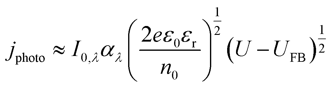 | (11) |
 | ||
| Fig. 7 Square of the photocurrent predicted by the Gärtner–Butler equation using αλ = 1.6 × 10⁷ m−1, I0,λ = 3.6 × 10²¹ m−2 s−1, εr = 80, n0 ≈ ND (for various doping levels), p0 ≈ 0, CH = 0.2 F m−2 and UFB = 0 for the cases of U − UFB = ΔϕSC + ΔϕH () and U − UFB ≈ ΔϕSC (–). | ||
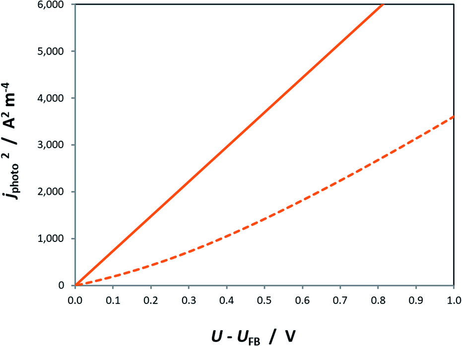 | ||
| Fig. 8 Square of the photocurrent predicted by the Gärtner–Butler equation using αλ = 1.6 × 10⁷ m−1, I0,λ = 3.6 × 10²¹ m−2 s−1, εr = 80, n0 ≈ ND = 1026 m−3, p0 ≈ 0, CH = 0.2 F m−2 and UFB = 0 for the cases of U − UFB = ΔϕSC + ΔϕH () and U − UFB ≈ ΔϕSC (–). | ||
While the formulation in eqn (10) and (11) is given for monochromatic light, it is possible to predict the photocurrent under white light illumination by integrating the product of the photon flux and absorption coefficient over the relevant wavelength range and employing their spectrally resolved values, as in eqn (12).29
Furthermore, most real systems will be affected by charge carrier recombination, which is a function of ΔϕSC. The charge transfer efficiency, which represents the fraction, Φ, of the theoretical maximum photocurrent, eIo, that is actually measured, needs to be factored in, as in eqn (12),29 because recombination can delay photocurrent onset to potentials well away from the flat band, as is often observed with water oxidation at metal oxide photoanodes.
Although it is possible to produce a semi-empirical description of Φ, experimental data are required to do so. Charge transfer efficiencies can be determined from photoelectrochemical impedance spectroscopy (PEIS) data,29,48 transient absorption spectroscopy (TAS)49,50 or intensity modulated photocurrent spectroscopy (IMPS),51 but these complicate the Gärtner–Butler method of flat band determination substantially. Alternatively, addition to the electrolyte of sacrificial reagents such as hydrogen peroxide,52 hydrogen sulfide53 or methanol,54 can increase dramatically the rates of charge transfer relative to those of recombination. This approach could increase confidence in the flat band potential value determined from eqn (10). However, even in the presence of sacrificial reagents, the charge transfer efficiency is not guaranteed to be unity near the flat band potential, so the problem shown in Fig. 8 may be further exacerbated.
 | (12) |
In the dark, a quasi-steady state current flows. Upon illumination, there is a transient photocurrent spike, followed by decay to a quasi-steady state photocurrent. When the light is turned off, similarly there is a transient spike in current, before decaying back to the steady state dark current, corresponding to a new electrode potential. Spikes in both dark currents and photocurrents are associated with capacitance charging of the interface.43 A spike in positive current is registered when illumination triggers an anodic photocurrent. Conversely, a spike in negative current is registered when illumination triggers a cathodic photocurrent. The flat band is identified as the potential at which the inversion between cathodic and anodic photocurrents occurs as this happens when the direction in band bending changes. This can be done through visual analysis of chopped photocurrent data, which will indicate the narrow potential region over which the transition takes place (as done in this study). Alternatively, the transition potential can be identified using a lock-in amplifier, which will evaluate transient photocurrents.
For the case of a n-type semiconductor, the principal photocurrent is expected to be anodic as illumination increases the concentration of holes substantially above the equilibrium value, whereas the effect is not as pronounced for electrons, especially if the semiconductor is heavily doped. However, in principle, a cathodic photocurrent may also be registered on a n-type semiconductor in the presence of a suitable redox couple,43 although a steady state cathodic photocurrent is considered unusual, especially if the concentration of donors, n0, is of the same order of magnitude as the density of states in the conduction band, NC.
This method for flat band determination has been proposed to be more accurate than using the Mott–Schottky equation, as measurements are not compromised by substantial rates of Faradaic processes.43 However, despite featuring in several studies,45,55,56 this technique is not used widely for this purpose.
Experimental
Photoanode fabrication
Undoped iron oxide films were prepared by spray pyrolysis of ethanol absolute (AnalaRNormapur, VWR BDH Prolabo) containing 0.1 mol FeIIICl3·6H2O dm−3 (Sigma Aldrich). This precursor solution was nebulised using compressed air onto fluorine-doped tin oxide (FTO) coated glass slides (TEC 8, Cytodiagnastics, Canada). The solution and the compressed air were introduced via separate flow channels into a quartz nebulizer (TQ+ Quartz Nebulizer, Meinhard, USA) at a flow rate and pressure of 1.68 × 10⁻² cm3 s−1 and 345 kPa, respectively. The nebulizer was mounted onto a CNC machine (HIGH-Z S-720, CNC-Technik, Heiz) in place of the milling tip; the movement of the nebulizer over the glass slides was software-automated (WinPC-NC CNC Soft-ware, BobCad-CAM, USA) and programmed to take place alternately length-wise and width-wise over the sample, ensuring uniform coating of the substrate.Prior to deposition, blank FTO slides were cleaned with ultrasound in acetone and washed in ultrapure H2O. Subsequently, the slides were placed on a hot plate positioned within the inner perimeter of the CNC machine and maintained at 480 °C during the coating process.
The glass slides were thermally treated in an oven (Elite Thermal Systems Ltd, UK) in air at 500 °C for one hour. The thickness of the films was determined to be 47 ± 6 nm using a stylus profilometer (TencorAlphastep 200 Automatic Step Profiler). The band gap of the samples was determined from transmittance measurements in the UV-Vis-NIR wavelength range.
A silicone-based varnish (Tropicalised varnish, RS-online, UK) was applied over a portion of the iron oxide to isolate an electroactive area of 3.5 (±0.1) × 3.0 (±0.1) mm2.
The nanostructure of such spray pyrolysed α-Fe2O3 films on FTO and other substrates was demonstrated in our earlier studies.44,66
Photoelectrochemical characterisation
Samples were assessed using a potentiostat/galvanostat (Autolab PGSTAT 30 + Frequency Response Analysis module, Eco Chemie, Netherlands). Electrochemical characterization was conducted on three samples (these were prepared simultaneously on three FTO substrates and tested in the same way to ensure reliability of results; they will be hitherto referred to as Sample 1, Sample 2 and Sample 3) in 1 mol NaOH dm−3 (pH ≈ 13.6) solution prepared from analytical grade anhydrous 99.99% NaOH pellets (Sigma Aldrich) and ultrapure H2O. When measurements were made in the presence of hydrogen peroxide ions, 0.5 M H2O2 was added to 1 M NaOH, assumed to produce HO2− ions, the pH remaining unchanged. The counter electrode was a Ti|Pt mesh. The FTO|α-Fe2O3 working electrode was polarized relative to a KClsat|AgCl|Ag reference electrode (Metrohm, UK), whose electrode potential is predicted as +0.197 V relative to SHE. We note that the stability of this reference electrode in strongly alkaline solution was expected to be compromised eventually by formation of Ag(OH)2− ions; however, its stability was confirmed using an analogous unused electrode both prior to and post experiments. All electrode potential values are henceforth quoted versus SHE.A spectrometer (Stellarnet, UV-VIS spectrometer, BLK-CXR) was used to measure the total irradiance of a 300 W Xe arc lamp (LOT-Oriel) as 2815 W m−2, of which 699 W m−2 was above the band gap of 2.2 eV. The use of AM1.5G radiation was not important in this study as the focus was not on material performance; intensities >1000 W m−2 were required to increase the resolution of some techniques.
The electrolyte was replaced following each set of impedance and photocurrent measurements to ensure any oxygen (and peroxide) species formed at anodic potentials did not impact on subsequent measurements by acting as hole or electron scavengers.
Electrochemical impedance spectroscopy
The EIS measurements were performed in the dark at potentials in the range −0.3 to +0.8 V (SHE). Each applied potential was perturbed sinusoidally by ±10 mV (p–p) at 75 frequencies in the range 10−1 to 105 Hz. Data was processed in Nova 1.11 (Autolab, Eco-Chemie, The Netherlands). Different equivalent circuits were explored for data fitting; a detailed description is provided in Sections 3 and 4 in the ESI.†Steady state and quasi-steady state photocurrent
Currents were recorded in the dark and under white light illumination as the electrode potential was swept from −0.5 V to +1.0 V vs. SHE at scan rates of 100, 50, 10, and 1 mV s−1. The net photocurrents were calculated according to jphoto = jtotal − jdark.Chopped photocurrent
Intensity-modulated currents were recorded when the hematite surface was exposed to light chopped at a frequency of 0.3 Hz as the potential was scanned from −0.5 V to +0.9 V (SHE) at scan rate of 1 mV s−1. The response was tested under chopped illumination by white light and by monochromatic light with wavelengths of 360, 450, 570, and 620 nm to identify any contributions to the photocurrent from inter-bandgap states.Light-saturated OCP
The open circuit potential was recorded under a range of illumination intensities (0–2815 W m−2). Intensity was controlled using neutral density filters (LOT-Quantum Design, Germany) with transmission factors: I/I0 = 0.01, 0.032, 0.16, 0.32, 0.50, 0.79 and 0.93. Stabilization of values required up to 30 minutes in 1 M NaOH solutions and ca. 6 minutes in solutions containing hydrogen peroxide. In one instance, the effect of dissolved oxygen was examined by comparing data in oxygenated and de-oxygenated 1 M NaOH electrolyte solutions. In the latter case, zero-grade nitrogen (99.998% and oxygen impurity removed, BOC) was bubbled through the electrolyte for 30 minutes prior to each OCP measurement.Results & discussion
Mott–Schottky analysis
Impedance data collected across the hematite|NaOH inter-face exhibited multiple time constants over the range of potentials examined, as shown in Nyquist and Bode phase plots in Fig. 9(a) and (b), respectively, for one of the three hematite samples.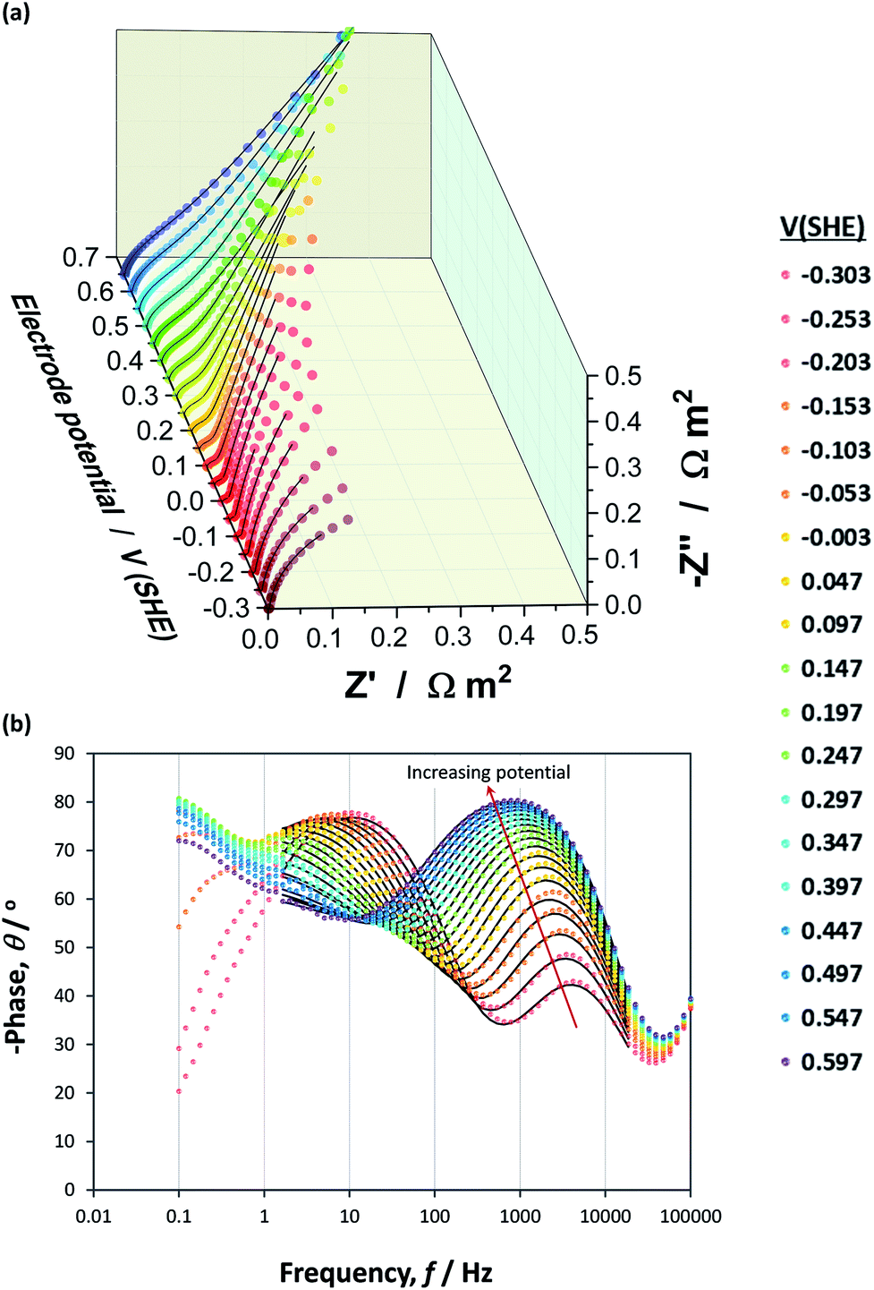 | ||
Fig. 9 Nyquist (a) and Bode phase (b) plots constructed from experimental  and simulated () EIS data obtained as a function of applied potential across an α-Fe2O3|1 M NaOH interface. and simulated () EIS data obtained as a function of applied potential across an α-Fe2O3|1 M NaOH interface. | ||
At high frequencies in the range ≈18.6–100 kHz, a very small impedance feature was detected that was invariant with applied potential. It was assumed to have been caused by the reference electrode67 and was neither affected by, nor impacted on, the interfacial capacitance, as shown in Fig. S8 in the ESI.† These impedance values were excluded from the circuit fittings.
The appearance of at least two convoluted semicircles in all Nyquist plots, demonstrated that the simplified circuit shown in Fig. 6 did not represent our α-Fe2O3|1 M NaOH interface accurately. Fig. 10 shows schematically several alternative circuits that have been used to describe how an additional charge trapping entity, such as a surface state or the back contact in the case of thin films, affects interfacial impedances. Mathematical formulations for the real and imaginary components of these four circuits are presented in Section 3 in the ESI† and the Nyquist plots are compared using identical values of RFaradaic, R1, C1, R2 and C2. Results show with certainty that only circuits (b) and (d) can account for our observations, and that R2 and C2 are responsible for the high impedance semicircle recorded at low frequencies. Furthermore, impedances generated by circuits (b) and (d) for the same set of parameters are indistinguishable when C1 ≪ C2, as is often assumed when the Mott–Schottky equation is applied to experimental data. However, when C1 ≈ C2, a marked difference is observed. We found that only circuit (d) could be fitted successfully to our data.
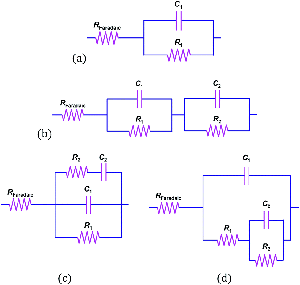 | ||
| Fig. 10 Equivalent circuits applicable to semiconductor|liquid interfaces in the dark. | ||
The fact that our data could be modelled using circuit (d) but not circuit (b), confirms that the additional capacitance (C2) was of the same order of magnitude as the semiconductor capacitance. Therefore, the existence of surface states seems possible. We also note that when C1 ≈ C2, there are few frequencies at which one might expect to isolate the contribution of the semiconductor; hence, without first examining a comprehensive set of impedance data, it is not recommended to construct Mott–Schottky plots from measurements taken at single frequencies.
EIS data, collected across the full range of applied potentials, were modelled using circuit (d) in Fig. 10, in which capacitors were replaced with constant phase elements. The details of subsequent CPE to Ceffective conversion are presented in Section 4 of the ESI.† The resultant Mott–Schottky plots for three hematite samples are shown in Fig. 11 (and bare FTO in Fig. S11†); these were generated assuming that C1 = CInterface = CSC. Correcting the intercepts by kBT/e to satisfy eqn (4) and accounting for dispersion between hematite samples, UFB = −0.68 ± 0.09 V (SHE).
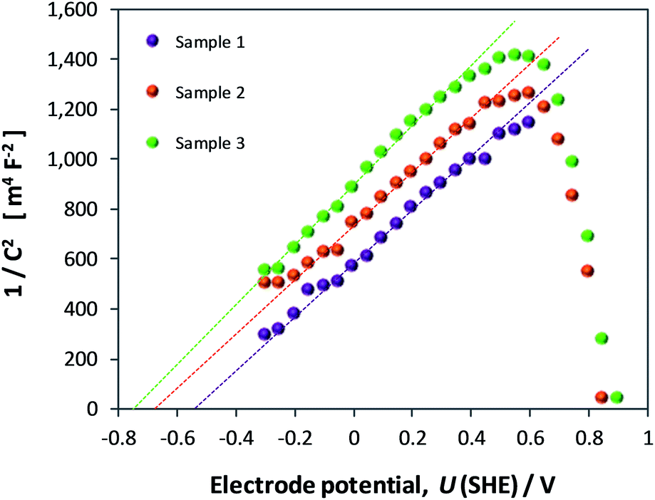 | ||
| Fig. 11 Mott–Schottky plots of interfacial capacitance derived from EIS data for three undoped hematite samples in 1 M NaOH (uncorrected by Helmholtz layer capacitance). | ||
If the Helmholtz capacitance is embedded in C1, as per eqn (3), then C1 needs to be corrected by CH to enable the determination of CSC. The result of correcting CInterface of one of the samples by a range of typically used values of CH (0.1–0.2 F m−2) is shown in Fig. 12. The large effect of CH demonstrates that our hematite samples must have had a high bulk electron density in the conduction band. Accounting for CH, the range of flat band potentials now becomes −0.77 to −0.32 V (SHE). Full details of calculations for 3 hematite samples is given in Section 6 of the ESI.†
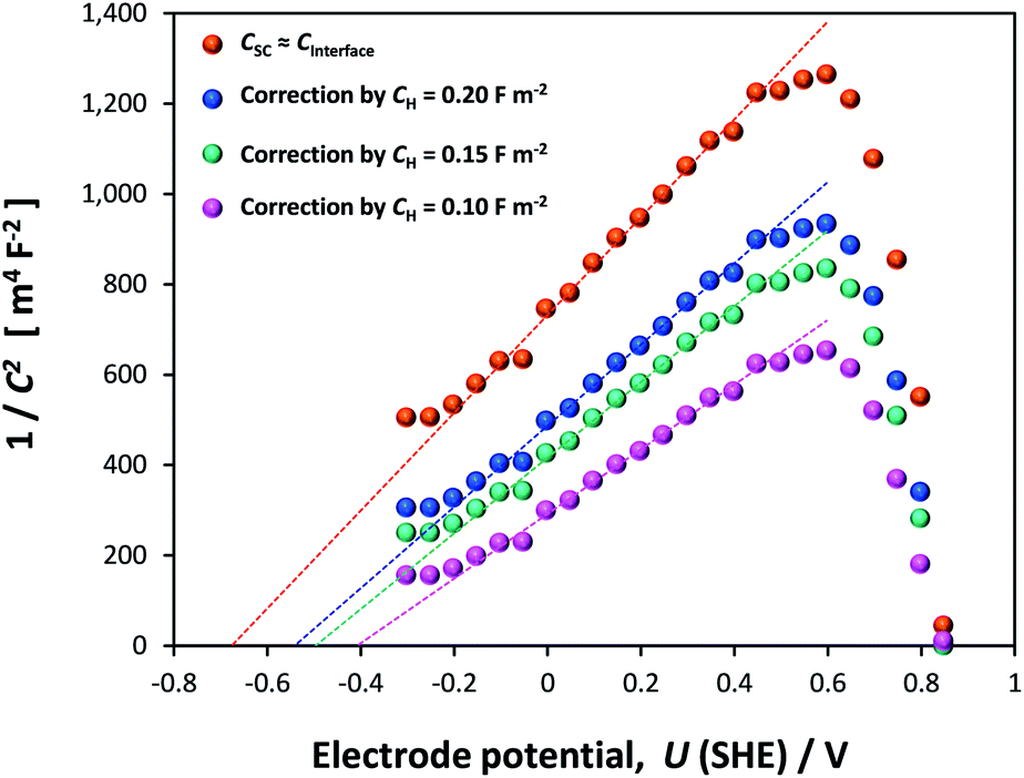 | ||
| Fig. 12 Mott–Schottky plots derived from EIS data of a single sample: in the first instance data is not corrected for the capacitance of the Helmholtz layer, and subsequently corrected using CH = 0.1, 0.15 and 0.2 F m−2. Dashed lines indicate extrapolations from which UFB were extracted. | ||
Dispersion in flat band potentials can be decreased successfully by applying the interfacial model, shown in Section 1 of the ESI,† to simulate the experimentally determined data. This enables the modelling of both CInterface and CSC using one value of flat band potential and one value of electron density. An example of the fitting is shown for one sample for different assumed values of CH in Fig. 13. Using this method, the range of UFB was narrowed down to −0.77 to −0.50 V (SHE) and range of n0 was 1.50 × 1025 to 1.70 × 1025 m−3, respectively. However, we consider the UFB uncertainty of 0.27 V to be large enough to require confirmation by other determination methods.
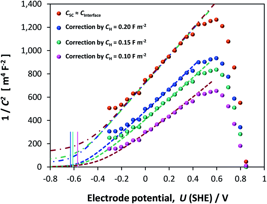 | ||
Fig. 13 Experimentally determined (●) and simulated Mott–Schottky plots based on semiconductor () and interfacial (![[dash dot, graph caption]](https://www.rsc.org/images/entities/char_e090.gif) ) capacitances. Vertical lines indicate computed UFB for the three assumed values of CH. ) capacitances. Vertical lines indicate computed UFB for the three assumed values of CH. | ||
Gärtner–Butler analysis
The flat band potentials determined through Gärtner–Butler analysis, were found to be in the range +0.24 to +0.34 V (SHE) in 1 M NaOH and −0.45 to −0.34 V (SHE) in the presence of H2O2, accounting for all potential scan rates. An example of the kinetics with and without H2O2, is shown in Fig. 14.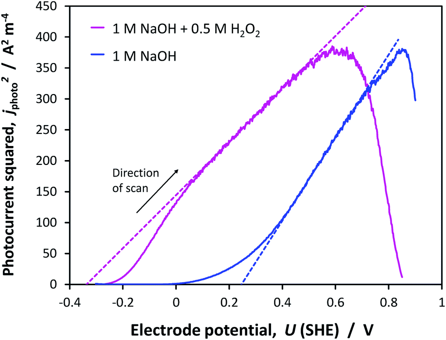 | ||
| Fig. 14 Net photocurrent squared on α-Fe2O3 as a function of applied potential (scan rate = 10 mV s−1) in the absence and presence of H2O2 hole scavenger. Dashed lines indicate extrapolations from which CFB were extracted. | ||
Full analysis of kinetics on all samples, including FTO, and in different electrolytes, is presented in Section 7 of the ESI.† The potential scan rate was found to have a minimal effect on UFB, causing a maximum dispersion of 0.03 V in the values obtained in 1 M NaOH and 0.05 V in the presence of H2O2.
The dramatic improvement in water oxidation kinetics in the presence of H2O2 shows the extent to which recombination rates hampered water oxidation on hematite and confirms that the Gärtner–Butler analysis always needs to be performed in the presence of a sacrificial reagent, unless charge transfer efficiencies can be quantified accurately using other methods. A degree of recombination is visible even with H2O2, as suggested by the ‘s’ shape of the jphoto2 curve at potentials close to the estimated flat band potential.
However, UFB values found with H2O2 were more positive than even the most positive values found through the Mott–Schottky method. If the electron density in the conduction band, estimated earlier using the interfacial model to be of order 1.50 × 1025 m−3, is correct, then the partial drop of applied potential across the Helmholtz layer, shown in Fig. 8, may have affected the flat band potential determined with the Gärtner–Butler analysis. With the available data, it is difficult to decide which of the Mott–Schottky or Gärtner–Butler analyses should be believed. Therefore, the results of other methods were still required for further confidence.
Chopped illumination
Transient photocurrents, measured on hematite during potentiodynamic scans under chopped illumination, showed two distinct regions. The first, at potentials >ca. −0.1 V (SHE) and shown in Fig. 15(a), was also measured under steady state and quasi steady state conditions, whereas a second anodic photocurrent, shown in Fig. 15(b), was evident at more negative potentials only under these transient conditions. This latter photocurrent has been shown previously to capture the existence of short-lived (millisecond to second lifetime) holes, which subsequently recombine with electrons even in the presence of anodic bias of several hundred millivolts. This rapid recombination tends to be explained with a possible presence of interfacial intraband surface states,48,68 which decrease the efficiency of charge separation in the space charge region. Alternatively, it has been shown using a combination of transient absorption spectroscopy50 and photocurrent transients that rapid decay in hole concentration is associated with a short pulse in cathodic current; such a current results when an accumulation of holes at the semiconductor surface causes a flux of bulk electrons back into space charge layer. This ‘back electron–hole recombination’ is dependent on the extent of band bending in the semiconductor, so the measurement of a steady state current is determined by the competition between the rates of water oxidation and recombination.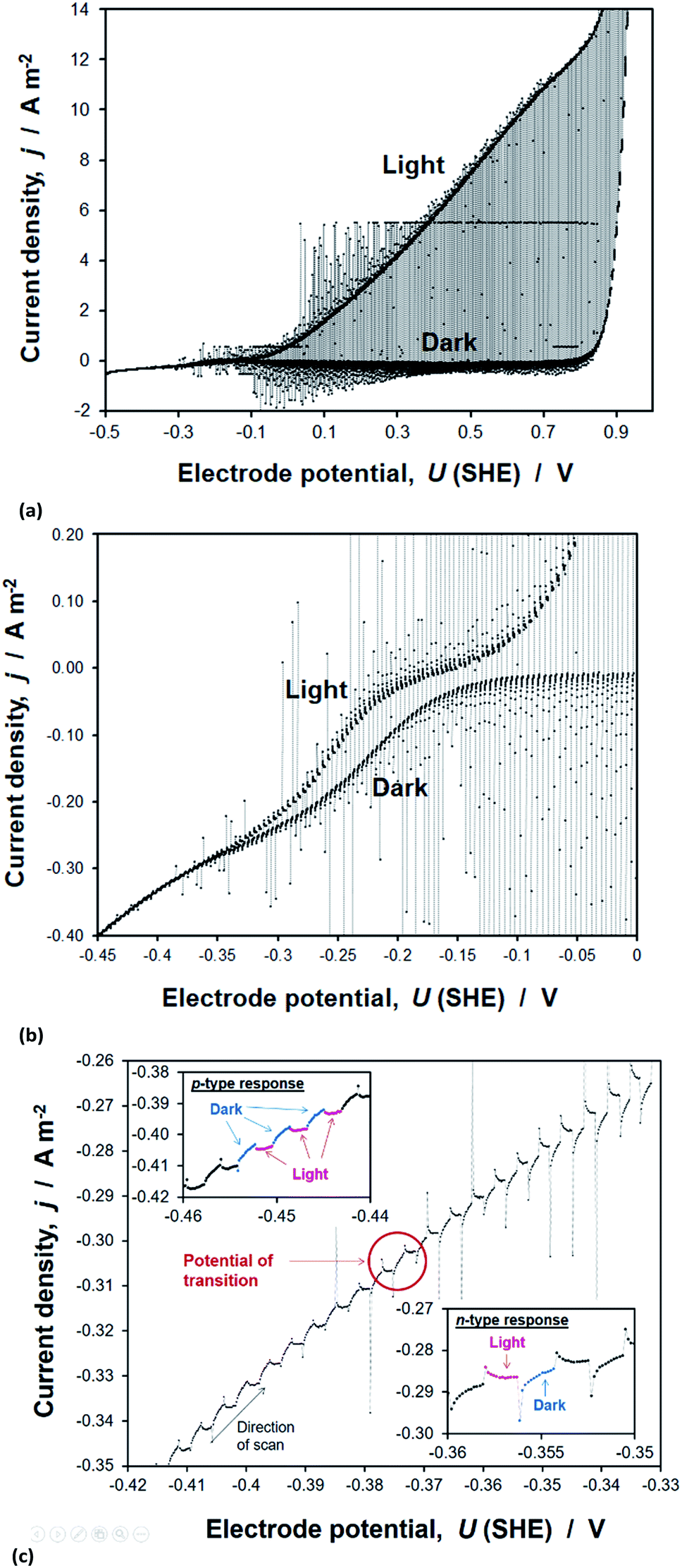 | ||
| Fig. 15 Chopped photocurrent on α-Fe2O3 in 1 M NaOH electrolyte, generated under white light illumination at a scan rate of 1 mV s−1 and with a chopping frequency of 0.3 Hz. (a), (b) and (c) show different sections of the data. | ||
The second photocurrent feature shown in Fig. 15(b) for electrode potentials <0.1 V (SHE) was not observed in the presence of H2O2, presumably because the rate coefficient for its oxidation was much greater than that of water, thereby minimising accumulation of holes at the surface and the resultant back electron–hole recombination rate. The data and analysis are presented in Section 8 of the ESI.†
The flat band potentials, determined from the potential at which photocurrent changes sign, as exemplified in Fig. 15(c), were in the range −0.40 to −0.38 V (SHE) in 1 M NaOH and −0.47 to −0.39 V (SHE) in the presence of H2O2. Therefore, it appears that, unlike in the Gärtner–Butler methodology, the presence of a hole scavenger is not strictly necessary for this method.
Over more than two decades, others have reported the potentials of photocurrent sign of transition on hematite, synthesised by different methods, to be ca. −0.3 V (1 M NaOH),56 −0.3 V (1 M KOH)55 and −0.4 V (1 M NaOH)45versus SHE. The dispersion in these estimates of flat band potentials and those determined within this work, is only 0.17 V. In contrast, the dispersion in UFB values from Mott–Schottky plots was 0.27 V within this study alone. Therefore, from the reproducibility point of view, we are inclined to place higher confidence in this method, than in using the Mott–Schottky equation.
Light-saturated OCP
The open circuit potential (OCP) of hematite recorded in 1 M NaOH with and without 0.5 M H2O2 is shown in Fig. 16 for one sample as a function of illumination intensity. Full data sets are shown in Section 9 of the ESI.† | ||
| Fig. 16 Effect of irradiance (0–2815 W m−2) and electrolyte composition on open circuit potentials of hematite. | ||
The OCPs in both electrolytes asymptoted unambiguously to limiting values in the range −0.15 to −0.12 V (SHE) in 1 M NaOH and −0.27 to −0.22 V (SHE) in the presence of H2O2. However, despite the minor dispersion between results obtained across all samples, it is clear that even the values obtained in H2O2 do not represent the flat band potential. Results obtained via GB and CI analyses show that UFB must lie at a more negative potential. Despite being a simple and elegant method theoretically, the complex nature of the semiconductor (especially an oxide)|liquid interface prevents full unbending of the bands upon irradiation. Analysis of EIS data from our α-Fe2O3 electrodes revealed unambiguously the presence of a source of extra capacitance at the interface. It is possible that this source results in a degree of Fermi level pinning when a bias potential is not applied externally. However, it would not have been possible to dismiss the results of the OCP method categorically without having evidence from the other three methods.
Comparison of methods
The objective of this work was to highlight the difficulties involved in the determination of the flat band potential of any semiconductor|liquid interface, especially when the semiconductor is nanostructured. We found that the challenge of estimating the flat band potential of such electrodes in aqueous media accurately cannot be understated. For the case of hematite, the challenge of estimating the flat band potential is exacerbated further by the unfortunate finding that only the categorically incorrect UFB values, such as those determined by OCP measurements and the Gärtner–Butler methodology in the absence of a hole scavenger, actually agree with the theoretical prediction in eqn (2).Through theory and experimental results with spray pyrolysed nanostructured hematite films, we concluded that the generation of Mott–Schottky plots from EIS data can be associated with too many uncertainties and relies heavily on speculation and assumptions. Even with a methodical and thorough approach to EIS analysis, our Mott–Schottky plots were not sufficiently convincing. Hence, we believe it to be an unreliable method, unless results are corroborated by other methods. Specifically, for highly doped n-type semiconductors, the contribution of the capacitance of the Helmholtz layer and associated potential drop are likely to result in a superficially negative flat band potential. Furthermore, the complex shapes of Mott–Schottky plots generated with experimental data mean that data should be collected over a wide potential range to ensure accurate extrapolation.
The Gärtner–Butler methodology is valid only when there is negligible electron–hole recombination, so it can only be applied to kinetics measured in the presence of charge scavengers. We found convincing agreement between results from the Gärtner–Butler methodology in the presence of H2O2 and the chopped photocurrent method, both with and without a hole scavenger. Combined, these methods show UFB to be in the range −0.47 to −0.34 V (SHE), allowing for different electrolyte compositions, potential scan rates and results from several samples. However, these values violate the theoretical criterion in eqn (1) if  is indeed +0.07 (±0.29) V (SHE) in 1 M NaOH.
The most uncertain contributor to the theoretical estimation of 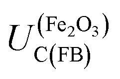 is the value of ΔϕH under the flat band condition. EIS results for our hematite samples provided strong evidence that the structure of the interface is complex and that there are multiple sources of capacitance. Hence, accurate estimation of ΔϕH requires further work and is likely to yield different values for different material compositions and synthesis methods.
Based on electron photoemission measurements on hematite, it has been suggested that the effective band gap is lower than the optical band gap22 due to the presence of Fe2+ polarons, which form the operative band edge for electron transfer. Such polarons could be formed either by over-doping with donors or via electronic contact with a material whose work function is at a higher energy than the energy of reaction (13).
| Fe3+ + e− → Fe2+ | (13) |
The hypothesis that electrons excited into the conduction band will not reside there, but will be trapped as polarons at a lower energy, may explain why the OCP measurements on hematite, such as presented in Fig. 16, asymptote to less negative potentials under intense illumination than those determined through the CI method. The polaron hypothesis was also accompanied by a re-evaluation of the hematite conduction band minimum, proposed to be ca. 0.5 eV higher22 than the previously assumed electron affinity value of −4.85 (±0.08) eV.69 A higher conduction band energy minimum may also explain why the flat band potentials determined in this study using the CI and GB methods were considerably more negative than those predicted by eqn (2). X-ray photoelectron spectra (XPS) obtained on hematite samples used in our study are shown and discussed in Section 11 of the ESI.† In practice, to maximise the accuracy of determining the flat band potential, the energies of the Fermi level and conduction and valence bands should be measured on the physical scale by some combination of Kelvin probe force microscopy (KPFM), XPS, ultraviolet photoemission spectroscopy (UPS) and UV-vis. This should lead to more accurate predictions of conduction and valence band edge potentials than currently possible with theoretical estimations based on the optical bandgap and electronegativity estimation. These experiments are recommended but were beyond the scope of this study as our primary focus was on highlighting the main issues with various electrochemical and photoelectrochemical measurements and data analyses.
On balance, the experimentally determined UFB values using the Gärtner–Butler (with scavenger) and chopped photocurrent methodologies were found to be the most convincing on our hematite samples. However, the extent is unknown to which the UFB values were superficially positive, due to the partial distribution of applied potential bias across the Helmholtz layer (Fig. 8).
There is no standard for accuracy or way of knowing the true flat band value. Hence, to enable greatest confidence in experimentally determined UFB values, we reiterate earlier advice38 that multiple methods should be employed for verification.
Conclusions
We have examined and estimated the flat band potential of hematite using the following methods:(a) MS – application of the Mott–Schottky equation to the interfacial capacitance, determined by electrochemical impedance spectroscopy as a function of applied potential and potential perturbation frequency;
(b) GB – Gärtner–Butler analysis of the square of the photocurrent as a function of applied potential;
(c) CI – determination of the potential of transition between cathodic and anodic photocurrents during slow potentiodynamic scans under chopped illumination;
(d) OCP – open circuit potential under high irradiance for the determination of the flat band potential of spray pyrolysed α-Fe2O3 photoanodes in 1 M NaOH solutions in the absence and presence of H2O2 hole scavenger.
Collectively, the four methods yielded flat band potential values in the range −0.77 to +0.34 V (SHE), illustrating clearly that some methods are highly inappropriate for characterising nanostructured materials.
Using experimental evidence, supported by modelling of the interface, we found the order of method accuracy on our hematite samples to be CI > MS > OCP > GB in the absence of hole scavengers, but CI > GB > MS > OCP if a hole scavenger was used.
Good agreement was found between results from the Gärtner–Butler methodology in the presence of H2O2 and the chopped photocurrent methodology both with and without a hole scavenger. Combined, these methods show UFB to be in the range −0.47 to −0.34 V (SHE), allowing for different electrolyte compositions, potential scan rates and results from multiple samples.
Mott–Schottky analysis is thought to yield superficially negative flat band potentials for highly doped n-type semiconductors. This is a result of the contribution of the Helmholtz layer to two aspects of the MS plot: (i) contribution of the Helmholtz layer capacitance to the measured interfacial capacitance, and (ii) partial distribution of the applied potential across the Helmholtz layer. The former stretches the MS plot along the y-axis and the latter stretches it along the x-axis, resulting in an overly negative x-axis intercept. Confidence in values determined by the MS method may be improved by com-paring capacitance values extracted from EIS data with those calculated using the interface model, with experimentally determined flat band potential and dopant density as inputs. Discrepancies between the data sets may help to determine the extent of the contribution from the Helmholtz layer capacitance, or otherwise indicate problems with capacitance evaluation. Concerns associated with analysis of impedance data and choice of equivalent circuit, as well as issues with differences between effective and geometric surface areas, serve to decrease confidence in flat band potentials determined using the MS method.
Gärtner–Butler analysis of oxidation kinetics on a n-type semiconductor in the absence of a hole scavenger, lead to superficially positive flat band potentials for two principal reasons: (i) recombination of photo-generated charge shifts the photocurrent onset potential away from the flat band potential, and (ii) kinetics are slower than predicted by the GB equation due to the partial distribution of applied potential across the Helmholtz layer. As with MS analysis, the extent of the latter issue can be estimated using an interfacial model, but this requires input of parameters, such as dopant density and dielectric constant which are not necessarily known a priori. Determination of the charge transfer efficiency is also possible using a variety of methods but is not trivial.
We conclude that multiple methods, including CI, should be employed to enable greatest confidence in experimentally determined UFB values.
Conflicts of interest
There are no conflicts to declare.Acknowledgements
The authors thank the UK Engineering and Physical Research Council for providing grants, supporting the PDRA position of A. H. and the studentship of J. C. A., and COLCIENCIAS Scholarship 568 for funding the studentship of F. E. B-L; Shell Global Solutions International B. V. for post-doctoral research associateships for A. H. and F. E. B-L. A. R. acknowledges the support from Imperial College London for her Imperial College Research Fellowship. The authors are also grateful to Dr Stephanie Pendlebury and Dr Florian Le Formal for helpful discussions.References
- A. J. Bard, R. Memming and B. Miller, Pure Appl. Chem., 1991, 63, 569 Search PubMed.
- M. Grätzel, Nature, 2001, 414, 338 CrossRef PubMed.
- N. Sato, in Electrochemistry at Metal and Semiconductor Electrodes, ed. N. Sato, Elsevier Science, Amsterdam, 1998, pp. 325–371, DOI:10.1016/B978-044482806-4/50010-6.
- Y. V. Pleskov and Y. Ya Gurevich, Semiconductor Photoelectrochemistry, Consultants Bureau, New York, 1986 Search PubMed.
- T. Zhai, X. Fang, M. Liao, X. Xu, H. Zeng, B. Yoshio and D. Golberg, Sensors, 2009, 9, 6504 CrossRef CAS PubMed.
- J. J. Gooding, Electrochim. Acta, 2005, 50, 3049–3060 CrossRef CAS.
- A. Kay, I. Cesar and M. Grätzel, J. Am. Chem. Soc., 2006, 128, 15714–15721 CrossRef CAS PubMed.
- Y. Ling and Y. Li, Part. Part. Syst. Charact., 2014, 31, 1113–1121 CrossRef CAS.
- H. K. Dunn, J. M. Feckl, A. Müller, D. Fattakhova-Rohlfing, S. G. Morehead, J. Roos, L. M. Peter, C. Scheu and T. Bein, Phys. Chem. Chem. Phys., 2014, 16, 24610–24620 RSC.
- Y. Ling, G. Wang, D. A. Wheeler, J. Z. Zhang and Y. Li, Nano Lett., 2011, 11, 2119–2125 CrossRef CAS PubMed.
- D. Wang, Y. Zhang, C. Peng, J. Wang, Q. Huang, S. Su, L. Wang, W. Huang and C. Fan, Adv. Sci., 2015, 2, 1500005 CrossRef PubMed.
- O. Zandi, A. R. Schon, H. Hajibabaei and T. W. Hamann, Chem. Mater., 2016, 28, 765–771 CrossRef CAS.
- K. Sivula, R. Zboril, F. Le Formal, R. Robert, A. Weidenkaff, J. Tucek, J. Frydrych and M. Grätzel, J. Am. Chem. Soc., 2010, 132, 7436–7444 CrossRef CAS PubMed.
- S. Sahai, A. Ikram, S. Rai, S. Dass, R. Shrivastav and V. R. Satsangi, Int. J. Hydrogen Energy, 2014, 39, 11860–11866 CrossRef CAS.
- J. Li, S. K. Cushing, D. Chu, P. Zheng, J. Bright, C. Castle, A. Manivannan and N. Wu, J. Mater. Res., 2016, 31, 1608–1615 CrossRef CAS.
- E. Thimsen, F. Le Formal, M. Grätzel and S. C. Warren, Nano Lett., 2011, 11, 35–43 CrossRef CAS PubMed.
- A. Hankin, J. C. Alexander and G. H. Kelsall, Phys. Chem. Chem. Phys., 2014, 16, 16176–16186 RSC.
- S. Trasatti, Pure Appl. Chem., 1986, 58, 955 CAS.
- A. J. Nozik, Annu. Rev. Phys. Chem., 1978, 29, 189–222 CrossRef CAS.
- M. A. Butler and D. S. Ginley, J. Electrochem. Soc., 1978, 125, 228–232 CrossRef CAS.
- R. S. Mulliken, J. Chem. Phys., 1934, 2, 782–793 CrossRef CAS.
- C. Lohaus, A. Klein and W. Jaegermann, Nat. Commun., 2018, 9, 4309 CrossRef PubMed.
- K. Uosaki and H. Kita, J. Electrochem. Soc., 1983, 130, 895–897 CrossRef CAS.
- R. De Gryse, W. P. Gomes, F. Cardon and J. Vennik, J. Electrochem. Soc., 1975, 122, 711–712 CrossRef CAS.
- D. C. Grahame, Chem. Rev., 1947, 41, 441–501 CrossRef CAS PubMed.
- N. E. Wisdom and N. Hackerman, J. Electrochem. Soc., 1963, 110, 318–325 CrossRef CAS.
- H. Gerischer, Electrochim. Acta, 1989, 34, 1005–1009 CrossRef.
- S. Onari, T. Arai and K. Kudo, Phys. Rev. B: Condens. Matter Mater. Phys., 1977, 16, 1717–1721 CrossRef CAS.
- A. Hankin, F. E. Bedoya-Lora, C. K. Ong, J. C. Alexander, F. Petter and G. H. Kelsall, Energy Environ. Sci., 2017, 10, 346–360 RSC.
- J. H. Kennedy and K. W. Frese, J. Electrochem. Soc., 1978, 125, 723–726 CrossRef CAS.
- R. K. Quinn, R. D. Nasby and R. J. Baughman, Mater. Res. Bull., 1976, 11, 1011–1017 CrossRef CAS.
- W. J. Albery, G. J. O'Shea and A. L. Smith, J. Chem. Soc., Faraday Trans., 1996, 92, 4083–4085 RSC.
- J. O. M. Bockris, Surface electrochemistry: a molecular level approach, Plenum, New York, London, 1993 Search PubMed.
- C. H. Hsu and F. Mansfeld, NACE-01090747, 2001, 57, 2.
- F. Cardon and W. P. Gomes, J. Phys. D: Appl. Phys., 1978, 11, L63 CrossRef CAS.
- Y. K. Gaudy and S. Haussener, J. Mater. Chem. A, 2016, 4, 3100–3114 RSC.
- D. Tiwari and D. J. Fermin, Electrochim. Acta, 2017, 254, 223–229 CrossRef CAS.
- H. O. Finklea, Semiconductor electrodes, Elsevier, Amsterdam, New York, 1988 Search PubMed.
- H. O. Finklea, J. Electrochem. Soc., 1982, 129, 2003–2008 CrossRef CAS.
- M. E. Orazem, inElectrochemical Impedance Spectroscopy, ECS Series of Texts and Monographs, ed. B. Tribollet, Wiley, Wiley-Interscience, Hoboken, N.J., 2008, vol. 48, http://https://www.wiley.com/en-us/Electrochemical+Impedance+Spectroscopy%2C+2nd+Edition-p-9781118527399 Search PubMed.
- E. C. Dutoit, R. L. van Meirhaeghe, F. Cardon and W. P. Gomes, Berichte der Bunsengesellschaft für physikalische Chemie, 1975, 79, 1206–1213 CrossRef CAS.
- K. S. Yun, S. M. Wilhelm, S. Kapusta and N. Hackerman, J. Electrochem. Soc., 1980, 127, 85–90 CrossRef CAS.
- S. M. Wilhelm, K. S. Yun, L. W. Ballenger and N. Hackerman, J. Electrochem. Soc., 1979, 126, 419–424 CrossRef CAS.
- F. E. Bedoya-Lora, A. Hankin, I. Holmes-Gentle, A. Regoutz, M. Nania, D. J. Payne, J. T. Cabral and G. H. Kelsall, Electrochim. Acta, 2017, 251, 1–11 CrossRef CAS.
- I. Cesar, K. Sivula, A. Kay, R. Zboril and M. Grätzel, J. Phys. Chem. C, 2009, 113, 772–782 CrossRef CAS.
- W. W. Gärtner, Phys. Rev., 1959, 116, 84–87 CrossRef.
- M. A. Butler, J. Appl. Phys., 1977, 48, 1914–1920 CrossRef CAS.
- K. G. Upul Wijayantha, S. Saremi-Yarahmadi and L. M. Peter, Phys. Chem. Chem. Phys., 2011, 13, 5264–5270 RSC.
- M. Barroso, S. R. Pendlebury, A. J. Cowan and J. R. Durrant, Chem. Sci., 2013, 4, 2724–2734 RSC.
- F. Le Formal, S. R. Pendlebury, M. Cornuz, S. D. Tilley, M. Grätzel and J. R. Durrant, J. Am. Chem. Soc., 2014, 136, 2564–2574 CrossRef CAS PubMed.
- D. Klotz, D. A. Grave and A. Rothschild, Phys. Chem. Chem. Phys., 2017, 19, 20383–20392 RSC.
- H. Dotan, K. Sivula, M. Grätzel, A. Rothschild and S. C. Warren, Energy Environ. Sci., 2011, 4, 958–964 RSC.
- F. Bedoya-Lora, A. Hankin and G. H. Kelsall, Electrochem. Commun., 2016, 68, 19–22 CrossRef CAS.
- C. A. Mesa, A. Kafizas, L. Francàs, S. R. Pendlebury, E. Pastor, Y. Ma, F. Le Formal, M. T. Mayer, M. Grätzel and J. R. Durrant, J. Am. Chem. Soc., 2017, 139, 11537–11543 CrossRef CAS PubMed.
- M. P. Dare-Edwards, J. B. Goodenough, A. Hamnett and P. R. Trevellick, J. Chem. Soc., Faraday Trans. 1, 1983, 79, 2027–2041 RSC.
- H. Wang and J. A. Turner, J. Electrochem. Soc., 2010, 157, F173–F178 CrossRef CAS.
- Y. V. Pleskov, V. M. Mazin, Y. E. Evstefeeva, V. P. Varnin, I. G. Teremetskaya and V. A. Laptev, Electrochem. Solid-State Lett., 2000, 3, 141–143 CrossRef CAS.
- R. Memming, Kinetics and Mechanisms of Electrode Processes, in Comprehensive Treatise of Electrochemistry, ed. B. E. Conway, J. O. M. Bockris, E. Yeager, S. U. M. Khan and R. E. White, Springer, USA, 1983, vol. 7, pp. 529–592 Search PubMed.
- J. A. Turner, J. Chem. Educ., 1983, 60, 327 CrossRef CAS.
- S. N. Frank and A. J. Bard, J. Am. Chem. Soc., 1975, 97, 7427–7433 CrossRef CAS.
- E. C. Dutoit, F. Cardon and W. P. Gomes, Berichte der Bunsengesellschaft für physikalische Chemie, 1976, 80, 475–481 CrossRef CAS.
- P. Salvador, Electrochim. Acta, 1992, 37, 957–971 CrossRef CAS.
- M. Turrión, B. Macht, H. Tributsch and P. Salvador, J. Phys. Chem. B, 2001, 105, 9732–9738 CrossRef.
- M. Turrión, J. Bisquert and P. Salvador, J. Phys. Chem. B, 2003, 107, 9397–9403 CrossRef.
- L. J. Handley and A. J. Bard, J. Electrochem. Soc., 1980, 127, 338–343 CrossRef CAS.
- C. K. Ong, S. Dennison, S. Fearn, K. Hellgardt and G. H. Kelsall, Electrochim. Acta, 2014, 125, 266–274 CrossRef CAS.
- F. Mansfeld, S. Lin, Y. C. Chen and H. Shih, J. Electrochem. Soc., 1988, 135, 906–907 CrossRef CAS.
- B. Klahr, S. Gimenez, F. Fabregat-Santiago, T. Hamann and J. Bisquert, J. Am. Chem. Soc., 2012, 134, 4294–4302 CrossRef CAS PubMed.
- M. A. A. Schoonen and Y. Xu, Am. Mineral., 2000, 85, 543–556 CrossRef.
Footnotes |
| † Electronic supplementary information (ESI) available. See DOI: 10.1039/c9ta09569a |
| ‡ Current address: Universidad de Antioquia, Medellín, Colombia. |
| § Current address: Arup, 13 Fitzroy St, London W1T 4BQ, UK. |
| ¶ Current address: Department of Chemistry, University College London, UK. |
| This journal is © The Royal Society of Chemistry 2019 |