
 Open Access Article
 This Open Access Article is licensed under a Creative Commons Attribution-Non Commercial 3.0 Unported Licence
Effect of solid-H2S gas reactions on CZTSSe thin film growth and photovoltaic properties of a 12.62% efficiency device†
Dae-Ho
Son
 ,
Seung-Hyun
Kim
,
Se-Yun
Kim
,
Young-Ill
Kim
,
Jun-Hyung
Sim
,
Si-Nae
Park
,
Dong-Hwan
Jeon
,
Dae-Kue
Hwang
,
Shi-Joon
Sung
,
Jin-Kyu
Kang
,
Kee-Jeong
Yang
* and
Dae-Hwan
Kim
*
,
Seung-Hyun
Kim
,
Se-Yun
Kim
,
Young-Ill
Kim
,
Jun-Hyung
Sim
,
Si-Nae
Park
,
Dong-Hwan
Jeon
,
Dae-Kue
Hwang
,
Shi-Joon
Sung
,
Jin-Kyu
Kang
,
Kee-Jeong
Yang
* and
Dae-Hwan
Kim
*
Division of Energy Technology, Daegu Gyeongbuk Institute of Science & Technology, 333 Techno jungang-daero, Hyeonpung-eup, Dalseong-gun, Daegu 42988, Republic of Korea. E-mail: monolith@dgist.ac.kr; kjyang@dgist.ac.kr; Fax: +82-53-785-3739; Tel: +82-53-785-3700
First published on 20th September 2019
Abstract
We fabricated CZTSSe thin films using optimized SLG-Mo/Zn/Cu/Sn (MZCT) as a stacked structure and described the phenomenon of Zn elemental volatilization using the MZCT stacked structure. We introduced H2S gas to effectively control the S/(S + Se) ratio of the film in the sulfo-selenization process and to suppress Zn volatilization. Unlike during the selenization process, a stable ZnSSe thin film was formed on the precursor surface during the sulfo-selenization process. The formation of the ZnSSe thin film inhibited Zn volatilization, which facilitated control of the thin film stoichiometry and played an important role in crystal growth. In addition, the sulfo-selenization process using H2S forms a grading of the S/(S + Se) ratio in the depth direction in the ZnSSe layer. The ZnSSe layer with this property causes the band gap grading in the CZTSSe absorption layer. Finally, through our optimized annealing process, we realized a world record CZTSSe solar cell with a certified power conversion efficiency of 12.62% and a centimetre-scale (1.1761 cm2) efficiency of 11.28%.
1. Introduction
In recent years, Cu2ZnSn(S,Se)4 (CZTSSe) has attracted much attention in the field of thin film solar cells. CZTSSe thin films show p-type conductivity, high light absorption coefficients of approximately 104 cm−1 and direct bandgaps of 1.0–1.5 eV.1–5 The theoretical solar conversion efficiency of CuZnSnS (CZTS)-based thin film solar cells is as high as 32.2%.6 However, the maximum conversion efficiencies reported for devices based on these materials are still far from those achieved with more mature CIGS technologies. The highest efficiency, i.e., 12.6%, for CZTSSe solar cells, which were produced using the hydrazine-based solution process, has not been broken since 2014.7 Various synthesis methods and efforts, such as defect control, passivation, grain growth, bandgap control and doping, have been attempted to enhance the solar cell performance, but efficiency results of 12% or higher are rare.8–13In general, CZTS and the related selenide CuZnSnSe (CZTSe) and CZTSSe thin films have been reported to be produced by a range of different routes, including the reaction of metal or sulfide precursors in a sulfur or selenium atmosphere and single-stage physical vapour deposition. We previously prepared CZTSSe thin films using sulfur compound precursors under elemental selenium ambient conditions in a sealed tube.14 The merits of this technique are as follows: (1) the sulfur in the compound precursor films is helpful for achieving good composition uniformity. (2) The deviation in the resulting metal compositions from those of the precursors after the selenization thermal process can be suppressed. (3) This technique shows good efficiency with the selenization-only process, and conducting the difficult sulfo-selenization process is not essential. (4) This technique can achieve the formation of a CZTSSe film without noticeable voids. In contrast, most of the CZTSSe absorbers produced using pure metal precursors have many pores, and elemental volatilization easily occurs during the heat treatment process.12,15–20 The element loss from the CZTSSe absorber bulk results in poor controllability in achieving the target stoichiometry, and ensuring high-efficiency device characteristics is difficult.21
Thus, the type and structure of the precursor must be optimized. The precursor stack ordering plays an important role in CZTSSe crystal growth and the performance of the corresponding cell.14 For example, six types of precursors with different stacking sequences were prepared by sequential deposition of Cu, Sn, and Zn.12 The resulting morphologies, phases and compositions of the resulting CZTSSe thin films were different for different stacking orders. In general, soda lime glass (SLG)/Mo/Sn/Zn/Cu and SLG/Mo/Zn/Sn/Cu precursor structures have been used in many studies,12,20 but obtaining uniform efficiency is difficult because of the bubble phenomenon that occurs on the thin film during the sulfo-selenization process (not shown here). We tried to fabricate uniform and high-efficiency CZTSSe solar cells using an optimal precursor structure because the order of each layer of the stack precursor has an important influence on the characteristics of the thin films and devices.
In addition, optimization of the heat treatment process is a key factor in CZTSSe synthesis. Many articles have been published on heat treatments, such as sulfurization, selenization and sulfo-selenization, to synthesize good quality CZTS system thin films.14,22,23 For most of the reported synthesized CZTSSe thin films with high efficiency, the bandgap of the absorber layer was controlled to optimize the characteristics.7,24 Various methods can be used to control the bandgap, and the bandgap is easily adjusted by controlling the composition ratio of S and Se in the CZTSSe thin film.20,25,26 In our previous study, a 12.3% efficiency CZTSSe solar cell was fabricated through a two-step process using a metal precursor.10 We found that the S/(S + Se) ratio can be controlled by using an appropriate SeS2/S weight ratio, and bandgap grading was observed in the depletion region of the CZTSSe absorber layer. Adjusting the bandgap of the light absorbing layer is a good method for increasing the open-circuit voltage. However, the SeS2 source is in powder form, is used in small amounts compared with Se, and evaporates first. Thus, uniformly distributing SeS2 in the sulfo-selenization process is difficult, and a uniform S supply method is needed to ensure process controllability.
In this work, we fabricate CZTSSe thin films using optimized SLG-Mo/Zn/Cu/Sn (MZCT) as a stacked structure and describe the volatilization phenomenon of the Zn element using the MZCT stacked structure. In general, the elements of the thin film deposited at the bottom of the precursor structure are expected to suffer less volatilization loss due to the existence of upper buffer layers.12 Since SnS and SnSe are materials with a significant vapour pressure above 400 °C, Sn is deposited on the bottom, and Zn is deposited on top, which makes removal of the Zn-related secondary phase on the surface easy. During the heat treatment process, Sn of the metal precursor naturally migrates to the lower side of the Mo interface due to the wetting phenomenon. More details on crystal growth have been discussed in other articles.27 Therefore, the Sn thin film does not need to be deposited on the bottom of the stack. Additionally, in our case, the Zn elemental loss is a major problem even though the Zn layer is deposited at the lowest position in the precursor stack order. In the pure selenization process, ZnSe nanowires are grown on top of the thin film by Zn volatilization, which is well explained by the vapour–liquid–solid (VLS) model; Zn loss and ZnSe nanowire growth on the surface make achieving a uniform interface and controlling the compositions of constituent elements difficult. Because of the difficulty in controlling the composition ratio and the formation of nanowires on the thin film, the CZTSe thin film does not have a p-type thin film stoichiometry, and a p–n junction is not formed due to the conductive characteristics of the absorber layer.
In addition, we introduce H2S gas instead of SeS2 to effectively control the S/(S + Se) ratio of the film in the sulfo-selenization process and to suppress Zn volatilization. The sulfur injection process using H2S gas is more uniform and reproducible than any other process using S or SeS2 powder. Unlike during the selenization process, a stable ZnSSe thin film is formed on the surface of the precursor during the sulfo-selenization process. The formation of the ZnSSe thin film inhibits Zn volatilization, which facilitates control of the thin film stoichiometry and plays an important role in crystal growth. Finally, through our optimization process, we realize a world record CZTSSe solar cell with a certified power conversion efficiency of 12.62%. Recently, our device results have been included in the solar cell efficiency tables (version 53) published in Progress in Photovoltaics (PIP).28 The Newport certified 1.176 cm2 device and 0.480 cm2 device show efficiencies of 11.3% and 12.6%, which were included in the recent PIP solar cell efficiency Tables 1 and 2,† respectively.28 In addition, DGIST achieved a device with an efficiency of 13.04% as certified by KIER (Korea Institute of Energy Research) in 2018 (see S1†). The 13.04% efficiency CZTSSe device fabrication process is almost identical to that for the 12.62% certified device, but the precursor thickness and H2S gas injection conditions are slightly different. However, because KIER is not a designated ISO/IEC 17025 certification centre, the efficiency record of 13.04% is unofficial.
2. Experimental section
2.1. Device fabrication
The precursor metal films were fabricated on molybdenum-coated SLG substrates. The metal precursor layers were sequentially deposited by sputtering 99.99% pure Cu, Zn, and Sn targets. The metal precursors with a Zn/Cu/Sn sequence were formed on the Mo-SLG substrates by DC sputtering at room temperature. The layers were deposited under sputtering powers of 300 W, 150 W, and 300 W for the Cu, Zn and Sn targets, respectively, at a working pressure of 1 mTorr in an Ar atmosphere. The thickness of each layer in the precursors was adjusted to control the final thickness of the CZTSSe film and the composition ratio. The metal precursors were reacted and annealed in annealing equipment. The annealing equipment had upper and lower halogen lamp heat sources, and the pressure inside the chamber could be adjusted through a throttle valve. The sample box system inside the annealing equipment consisted of a sample holder, a quartz boat and a quartz cover (see S2†). The precursor sample holder was made of the graphite material. The quartz boat was located under the precursor sample holder. The selenization process could be performed by placing Se in the quartz boat. The abovementioned holder system was placed inside the heat treatment equipment, and the selenization or sulfo-selenization process was carried out. First, the inside of the chamber was evacuated to a base pressure. Next, 2000 sccm of Ar gas and 200 sccm of H2S gas (diluted with 90 vol% Ar) were simultaneously injected. When the pressure reached 700 Torr, all gas supply was stopped, and the heating process was performed. The internal chamber pressure during the heating process was maintained at 700 Torr by an automatic pressure controller without additional gas supply. In the pure selenization process, only Ar gas was injected without supplying H2S gas.The growth of CZTSSe thin films from precursors is strongly influenced by the temperature, precursor composition ratio and annealing atmosphere. The heating profile was optimized by the trial and error approach while the conditions, such as the reaction source and process pressure, were changed.10 The optimized internal heating profile of our selenization process exhibited two annealing steps. The detailed temperature profiles are presented in S3.† To fabricate solar cells, the obtained absorber layers were covered with a 50 nm-thick CdS buffer layer by chemical bath deposition. Then, a 50 nm intrinsic ZnO layer and a 300 nm Al-doped ZnO layer were deposited by RF sputtering. Finally, a 20 nm-thick Ni and 2 μm-thick Al grid was deposited via e-beam evaporation, and 110 nm-thick MgF2 was deposited by an e-beam evaporator. The designated cell area was defined by mechanical scribing to be ∼0.5 cm2.
2.2. Characterization and analysis
Surface images of the absorber layers were obtained by scanning electron microscopy (SEM) (Hitachi Co., model S-4800), and scanning transmission electron microscopy-energy dispersive spectrometry (STEM-EDS) measurements were performed using a QUANTAX-200 (Bruker Co.) to analyse the compositions of the absorber layers and map the distributions of the secondary phases. ICP measurements were taken with an ICPS-8100 (Shimadzu Co.) to analyse the compositions of the absorber layers. CZTSe-based devices were characterized to obtain optoelectronic properties, including the 1.5 AM illuminated J–V characteristics (94022A solar simulator, Newport Co.), dark J–V characteristics (Keithley 4200 semiconductor characterization system) and external quantum efficiency (EQE – Newport Quantx-300 System). Capacitance–voltage (C–V) and drive-level capacitance profiling (DLCP) measurements were also carried out with an LCR meter (E4980A, Agilent) to estimate the space charge width and carrier density.3. Results and discussion
3.1. The role of H2S in the annealing process of the MZCT precursor structure
Using the precursor structure of MZCT, we observed changes in the crystal phases of the thin films obtained through the pure selenization process without H2S gas supply. Surface and cross-sectional SEM micrographs of the annealed films are shown in Fig. 1. The samples were cooled down at the specific points along the optimized annealing temperature profile shown in Fig. S2.† The film cooled immediately after reaching 300 °C exhibits an almost metallic form without volume expansion (Fig. 1(a)). As the temperature increased (Fig. 1(b)–(g)), a nanowire-shaped phase grew on the thin film. At 360 °C, for a 0 min nominal annealing time (Fig. 1(b)), nanowires partially formed on the film, and the nanowires were observed mostly in the area of the surface edge contacting the graphite sample holder. This phenomenon occurred because the temperature at the edge of the sample is higher than that in the central region due to the heat transfer from the graphite holder surface. Samples and holders as observed with the naked eye are described in detail in S4.† Although the composition ratio of the precursor is Cu-poor and Zn-rich, the CZTSe films synthesized through selenization under an Ar atmosphere show Cu-poor and Zn-poor compositions. In other words, in the pure selenization process, Zn, which is the lowest layer of the precursor, is volatilized, and a ZnSe substance is attached to the surface of quartz through the selenization reaction. Zn volatilization and nanowire growth on the thin film were clearly observed after maintenance at 300 °C for 15 min.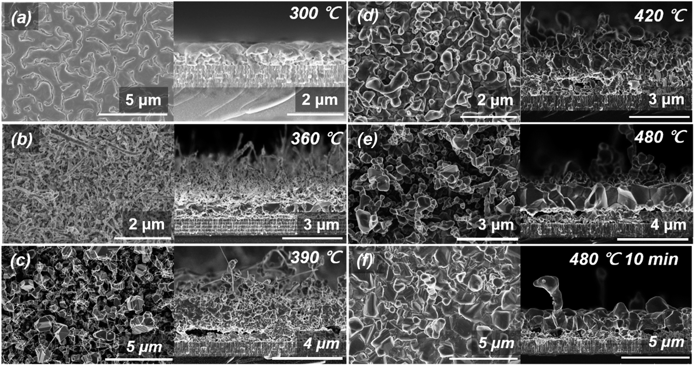 | ||
| Fig. 1 Surface and cross-sectional SEM images of CZTSe thin films obtained through the pure selenization process at 300 °C (a), 360 °C (b) 390 °C (c), 420 °C (d), 480 °C (e) and 480 °C for 10 min (f). For these samples, the reactive annealing was interrupted at the indicated temperature along the temperature profile. | ||
Fig. 2 shows SEM images of the surface and cross-section of the thin films formed according to the annealing temperature under the conditions of introducing H2S gas and selenium granules (approximately 200 mg) and using the same precursor. During the sulfo-selenization process with increasing temperature, the CZTS formation reaction clearly appears. Unlike IBM's 12.6% CZTSSe thin film surface morphology, the grain surface of our CZTSSe thin film is relatively round because of the low sulfur ratio of the thin film. In the sulfo-selenization process with H2S gas supply, the growth of nanowires was not observed during the heat treatment process, and ZnSSe was not adhered to the quartz cover facing the precursor. Thus, the volatilization of Zn was expected to be well controlled by H2S gas during the sulfo-selenization process. As shown in Fig. 2, no other abnormal phase was found in the upper crystalline region of the CZTSSe absorber layer synthesized in the sulfo-selenization process in which Zn vapourization was suppressed. To analyse and verify the phenomenon in which Zn volatilization does not occur, we performed STEM and mapping analyses.
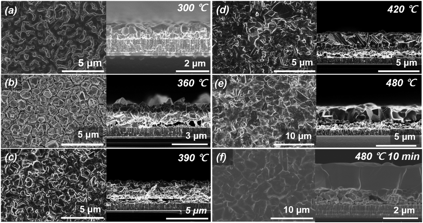 | ||
| Fig. 2 Surface and cross-sectional SEM images of CZTSSe thin films obtained through the sulfo-selenization process at 300 °C (a), 360 °C (b) 390 °C (c), 420 °C (d), 480 °C (e) and 480 °C for 10 min (f). For these samples, the reactive annealing was interrupted at the indicated temperature along the heat temperature profile. | ||
Fig. 3(a) shows STEM and EDS mapping images of the thin film obtained after a maintenance period of 15 min at 300 °C under the condition of no H2S gas injection. In the EDS mapping results, almost no Zn–Sn alloy is observed, only Cu–Sn and Cu–Zn alloys. The Cu–Zn alloy has phases ranging across the entire binary phase diagram, such as β-CuZn, γ-Cu5Zn8, and ε-CuZn5.29 Among them, Cu5Zn8 is a strongly stable phase at room temperature, and thus, the Cu–Zn alloy with this phase easily forms. For this reason, the formation of the Cu–Zn alloy preferentially occurs over that of the Cu–Sn alloy. After formation of the Cu–Zn alloy, the excess Cu in the upper part forms an alloy with some of the Sn, and the unreacted Sn is mainly located near the Mo electrode. A portion of the Zn is selenized to form a thin ZnSe layer that covers the metal alloy. To more precisely examine the grain surface of the thin film, the upper part of Fig. 3(b) was enlarged and analysed by STEM and EDS mapping. In the results of Fig. 3(b), Cu–Zn and Cu–Sn alloys and some Sn are easily distinguished. Interestingly, a thin ZnSe shell was formed on the surface of both the Cu–Zn and Cu–Sn alloys, and nanowires were formed on the ZnSe layer. The length of the nanowire was greater than several tens of nanometres, and the nanowires were irregularly formed on top of the ZnSe thin film. Additional TEM analyses were performed to confirm the nanowire formation mechanism. Fig. 3(c)–(e) show more enlarged cross-sectional STEM images of the sample annealed at 300 °C for 15 min without H2S injection. Fig. 3(f) shows cross-sectional STEM-EDS mapping images. A Sn mixed metal droplet is present at the end of one of the nanowires in Fig. 3(f), and the wire is made of Zn–Se. Generally, the VLS mechanism is the most widely accepted growth mechanism.30,31 A catalyst nanoparticle is assumed to assist the growth and control of the diameter of the nanowire. Based on our STEM results, Sn is the catalyst nanoparticle that helps ZnSe nanowire growth. Above a certain temperature, the catalyst nanoparticle becomes liquid and is exposed to the vapour of the growing nanowire material. Since the eutectic point of Sn–Zn is approximately 200 °C, a liquid droplet of Sn–Zn can be formed at 300 °C. A droplet consisting of Sn is observed at the end of the nanowire. Additionally, since Zn has high vapour pressure characteristics, it can volatilize at 250 °C and act as a vapour phase source, and the formed nanowires are composed of Zn–Sn.32,33 Therefore, the VLS model can be applied. The kinetics of the VLS mechanism consists of four steps: (1) mass transport in the gas phase; (2) chemical reaction at the vapour–liquid interface; (3) diffusion in the liquid phase; and (4) incorporation of atoms into a crystal lattice.31 During the mass transport in the gas phase, the Zn content of the Sn–Zn alloy liquid droplets can be increased by the continuous diffusion of the Zn vapour phase due to the wide solubility limit at 300 °C. When Zn in the gas phase is continuously generated and diffused into a liquid Sn–Zn droplet, Zn segregation from the Sn–Zn droplet continuously occurs. The segregated Zn component reacts with Se vapour to form a Zn–Se nanowire, and a possible growth scenario is shown in Fig. 4. The ratio of the Zn–Se nanowire was observed to correspond to a metallic phase (an almost 2![[thin space (1/6-em)]](https://www.rsc.org/images/entities/char_2009.gif) :1 Zn:Se ratio), as shown in S5.† As seen from the above results, if the Zn volatilization cannot be suppressed, then the Zn–Se nanowire reacts with Se and continues to grow. Even if the thickness of Zn in the precursor is increased to compensate for the loss due to the Zn volatilization, good quality CZTSe cannot be obtained in our system because a portion of Zn will still vapourize and participate in the formation reaction of Zn–Se nanowires, which could induce compositional nonuniformity or secondary phases. If sufficient selenization of Zn is possible before Zn is volatilized, then Zn volatilization may be suppressed. However, the selenization process using selenium shots does not produce highly reactive selenium gas at low temperatures and thus does not form a ZnSe layer before Zn is volatilized. Thus, suppression of Zn volatilization in the selenization process is difficult.
:1 Zn:Se ratio), as shown in S5.† As seen from the above results, if the Zn volatilization cannot be suppressed, then the Zn–Se nanowire reacts with Se and continues to grow. Even if the thickness of Zn in the precursor is increased to compensate for the loss due to the Zn volatilization, good quality CZTSe cannot be obtained in our system because a portion of Zn will still vapourize and participate in the formation reaction of Zn–Se nanowires, which could induce compositional nonuniformity or secondary phases. If sufficient selenization of Zn is possible before Zn is volatilized, then Zn volatilization may be suppressed. However, the selenization process using selenium shots does not produce highly reactive selenium gas at low temperatures and thus does not form a ZnSe layer before Zn is volatilized. Thus, suppression of Zn volatilization in the selenization process is difficult.
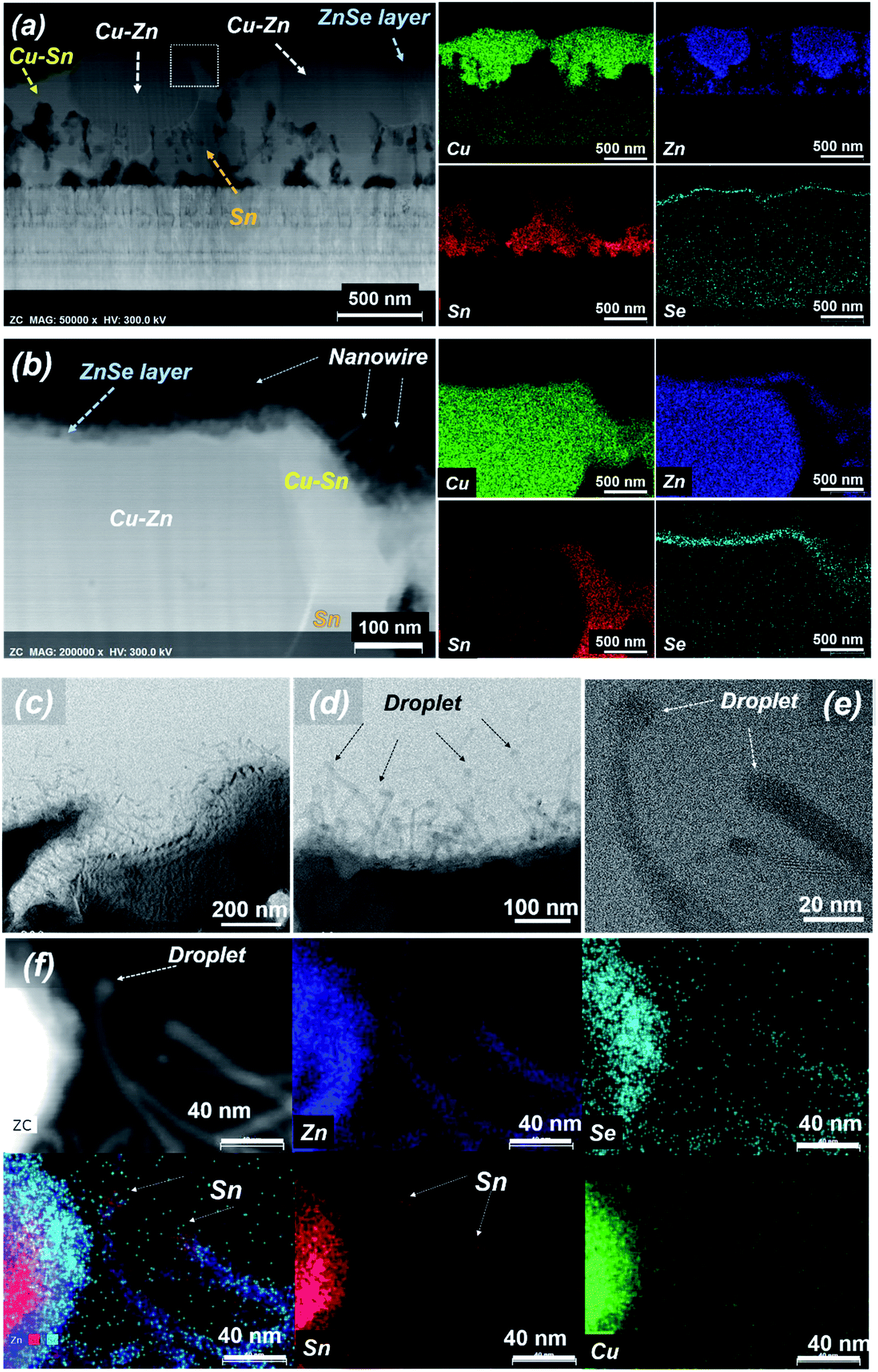 | ||
| Fig. 3 STEM and EDS mapping images of the thin film annealed for 15 min at 300 °C, and (b) photograph of an enlarged portion of the upper dotted white line box area in the STEM image of (a). (c), (d) and (e) STEM images of the thin film annealed at 300 °C for 15 min. (f) Image of a nanowire near the surface, and the corresponding elemental mapping results, obtained from the STEM-EDS image. | ||
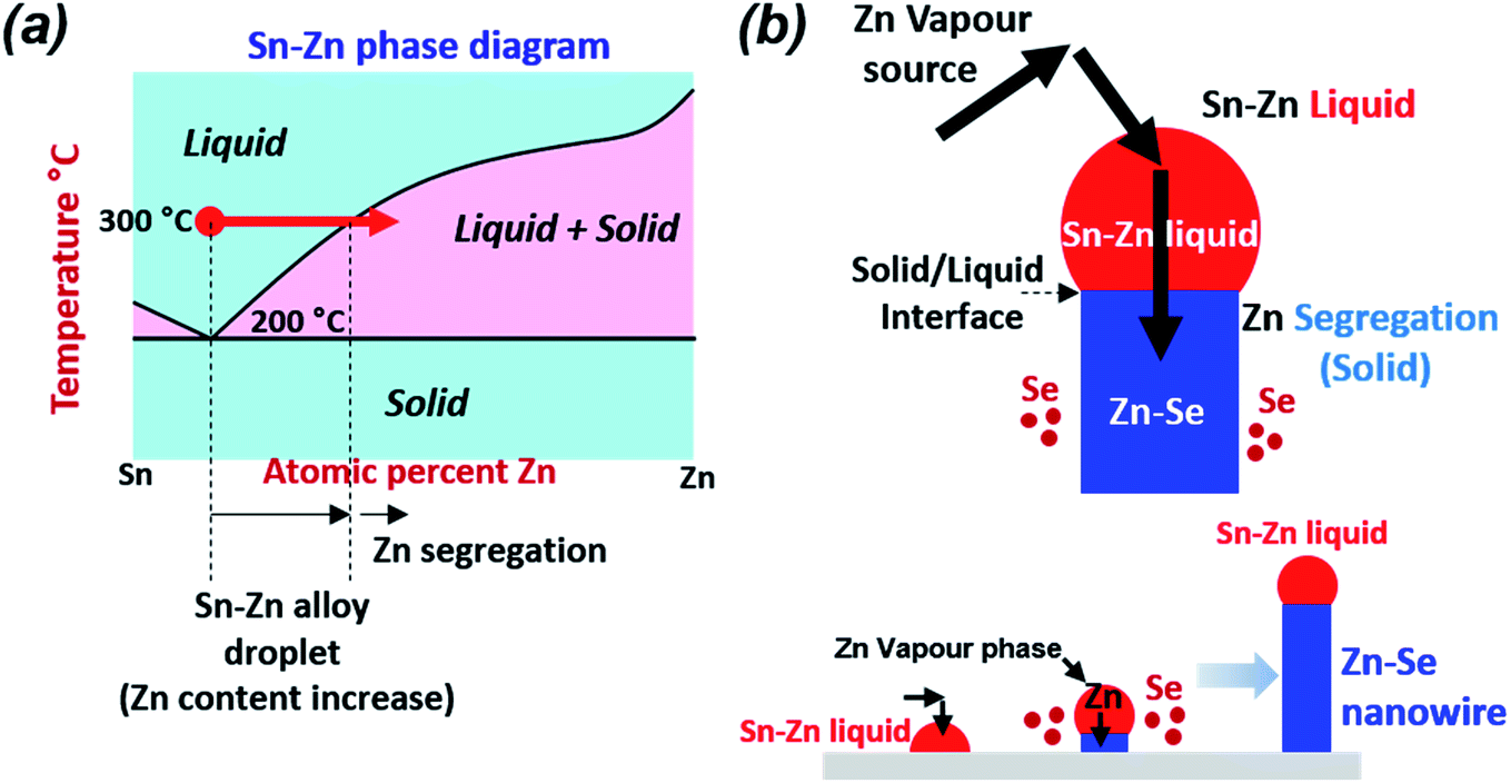 | ||
| Fig. 4 (a) Phase diagram of the Sn–Zn system indicating the composition of the liquid alloy39 and (b) schematic diagram of tin-particle-guided growth of ZnSe nanowires, according to the VLS model. | ||
The CZTSSe thin films obtained through the heat treatment process with H2S gas supply showed different results compared to the condition without H2S gas supply. The upper cross-sectional STEM-EDS mapping images of the samples cooled immediately after they reached 300 °C, 330 °C and 400 °C are shown in Fig. 5. Similar to the selenization process, the upper Zn layer was found to be chalcogenated by reaction with S and Se during the crystal reaction, and this ZnSSe layer exists in the form of a shell covering the underlying alloy, i.e., Cu–Zn and Sn–Cu, as shown in Fig. 5. As the annealing temperature increased, the thickness of the ZnSSe layer increased. As shown in the energy dispersive X-ray spectroscopy (EDX) line scan data in Fig. 5(d) and (e), the ZnSSe layer from the top to the bottom across the annealed thin film had a gradient of S and Se. This gradient phenomenon arose from the inconstant sulfur partial pressure conditions during the sulfo-selenization process. At the initial stage of sulfo-selenization, the highly reactive H2S gas easily reacts with the Zn of the metal precursor. As the temperature increases during the sulfo-selenization process, the Se partial pressure increases due to the active vapourization of Se granules, and a ZnSSe layer is formed. Even at 300 °C, a thick ZnSSe layer of approximately 50 nm was uniformly formed. Thermodynamically, since the reaction of Zn with S is more reactive than that of Zn with Se, the dense Zn–S phase is preferentially formed by the reactive H2S gas.34 In addition, due to the formation of the ZnS phase at the early stage below 300 °C, Zn volatilization and thus ZnSe nanowire formation do not occur. In the case of Se-only annealing, ZnSe shell formation is delayed and Zn actively vapourizes. Conversely, when Se annealing is combined with H2S gas supply, the Zn chalcogenide is relatively well formed, thus minimizing the Zn loss, and as a result, ZnSe nanowires are not observed. Consequently, the stoichiometry of the precursor and microstructure of CZTSSe can be controlled using reactive H2S gas. In our experience, loss of precursor elements during selenization or sulfo-selenization is problematic for the composition and phase control of CZTSSe absorbers. Therefore, the inhibition of constituent element vapourization is very important in a reliable and repeatable CZTSSe 2-step process.
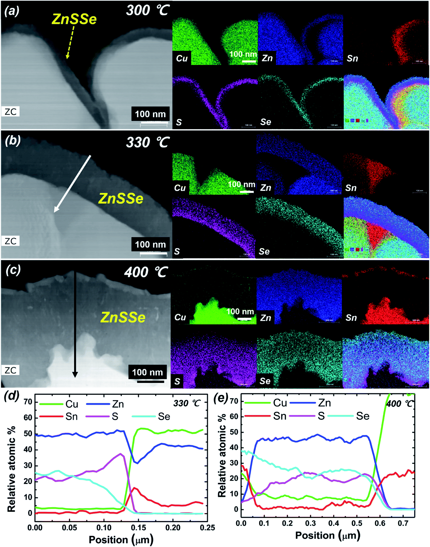 | ||
| Fig. 5 Cross-sectional STEM-EDS mapping images (a–c) of the CZTSSe thin films obtained through the sulfo-selenization process. For these samples, the reactive annealing was interrupted at the indicated temperature along the heat temperature profile. (d) and (e) Elemental profiles determined by EDX line scans. The scanning directions of (d) and (e) are the same as the arrow directions in (b) and (c), respectively. | ||
3.2. The CZTSSe thin film fabricated using the MZCT precursor structure and characteristics of CZTSSe solar cells
To investigate the structure and phase of the sister cell of the champion device (i.e., also exhibiting an efficiency of >12%), a CZTSSe cell cross-sectioned by a focused ion beam was investigated by STEM. Fig. 6(a) and (b) show cross-sectional STEM and EDS mapping images of the device that has undergone the same process as the best efficiency cell. Fig. 6(c)–(e) depict the element profiling results of the EDX line scans along the three arrow directions shown in Fig. 6(a). Remarkably, because of the considerable amount of void formation, an unintentional local contact structure was formed; a small fraction of upper CZTSSe was directly connected to the back contact through bridging of CZTSSe (lower CZTSSe), and a large portion of CZTSSe was formed on wide bandgap ZnSSe or voids. This seemingly poor structure could help reduce interface recombination near the back contact owing to the passivation effect of the wide bandgap ZnSSe layer. CuSn and Zn-related secondary phases were observed in the lower and upper parts of the void, respectively. In particular, the Zn-related secondary phase ZnSSe exists across the entire region between the upper CZTSSe and voids with a thickness of approximately 100–300 nm. In addition, an approximately 300 nm Mo(S,Se)2 interfacial layer is evident between the CZTSSe absorber layer and the Mo back electrode. Similar results were obtained when TEM analyses were repeated on samples produced by our 2-step CZTSSe process. Regarding the composition of the elements from the upper part to the lower part of the CZTSSe absorber layer in Fig. 6(c), the composition of sulfur slightly increases in the direction of the back electrode, but the composition of selenium decreases. More detailed composition changes are shown in S6.† As shown in Fig. 6(d) and (e), the upper and lower S/(S + Se) ratios in the dense CZTSSe thin films are different. The sulfur composition is high in the lower region near the Zn-related secondary phase, and the selenium ratio is higher in the upper region. The difference in the S/(S + Se) ratios in the CZTSSe absorber layer is closely related to the reaction of H2S gas with Zn from dezincification before formation of CZTSSe. Since ZnSSe initially reacts with H2S, it has a relatively large amount of S. Therefore, CZTSSe near ZnSSe has more S than CZTSSe near the junction, resulting in a natural back-surface graded bandgap structure, which is defined as an increase in the bandgap towards the back of the absorber layer. The difference in the composition of S/(S + Se) ratios in the CZTSSe absorber layer can be found in S6.† The back-surface graded bandgap structure establishes an additional drift field for the minority electrons that assist carrier collection and reduces back contact recombination.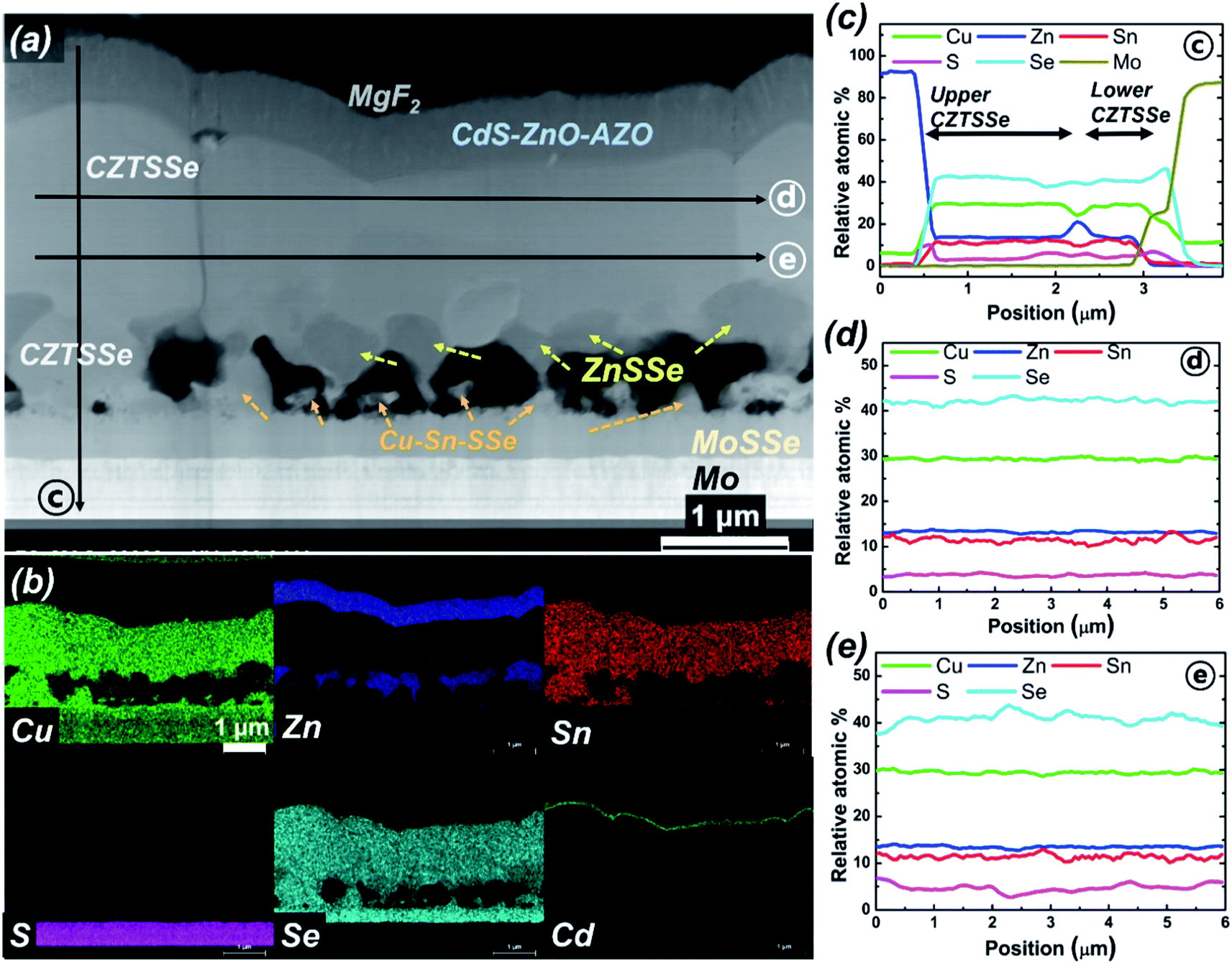 | ||
| Fig. 6 Cross-sectional STEM-EDS mapping images (a and b) of the sister cell of the champion CZTSSe thin film solar cell. (c)–(e) Elemental profiles determined by EDX line scans. The scanning direction of (c) is the same as arrow direction ⓒ in (a). The scanning directions of (d) and (e) are the same as arrow directions ⓓ and ⓔ in (a), respectively. | ||
Solar cell devices were fabricated with CZTSSe thin films grown using the MZCT structure in the sulfo-selenization process using H2S gas. The performance characteristics from 10 solar cells were statistically summarized and are shown as box charts in Fig. 7(a). The performance of the most efficient device was independently certified by the Newport Corporation, one of the recognized test centres, under standard test conditions (see S7†).35 Furthermore, DGIST received the test results of a different device, fabricated via a process similar to that for the 12.62% device, showing an efficiency of 13.04% from KIER, the renowned test centre in Korea, although not a so-called designated test centre (see S1†). Since 13.04% is not a certified value at the designated centres, we will discuss only 12.62%-related devices below. The measured current density–voltage and EQE characteristics are shown in Fig. 7(b) and (c), respectively. Our certified power conversion efficiency of the 0.4804 cm2 CZTSSe cell is 12.62%, with a corresponding VOC of 541.1 mV, a JSC of 35.38 mA cm−2 and an F.F. of 65.9%. Our result is 0.01% higher than the world record efficiency of IBM. Since the official best efficiency in the PIP solar cell efficiency tables ver. 53 uses the value rounded to the second decimal place, we can say that we achieved a ‘tie’ in world record efficiency; the rounded value is 12.6%, which is the same as that for IBM. However, our champion device area is larger compared to IBM's device (0.4209 cm2). As shown in Table 1, the current champion device has an open-circuit voltage that is improved by 28 mV and a current that is improved by 0.17 mA cm−2 compared to IBM's device. However, the F.F. is lower and is expected to improve in the near future through the modification of the buffer, TCO and back contact processes. The values of the extracted diode parameters and characteristics, such as Gs, Rs, A, J0, Eg and Eg/(q − VOC), compared to those of the IBM device are shown in Table 1. The slope of the J–V curve measured under illumination is very small in the shunt resistance measurement range and is not accurate due to differential noise, but the shunt conductance value of our device is smaller than that of the IBM device. The values of Rs, A, and J0 extracted from the IBM device are excellent, and this device therefore exhibits a higher F.F. Additionally, A > 1 implies that in addition to the ideal recombination in the quasineutral p- and n-regions, nonideal recombination also occurs in the space charge region (SCR) of the p–n junction.36 The low F.F. value of our CZTSSe device indicates that the p–n junction diode quality needs to be increased by reducing recombination in the SCR region. Despite the low F.F. of the champion device, the VOC deficit, equal to the difference between the bandgap and VOC, is reduced compared to IBM′s device. Among the reported CZTSSe devices, the champion device has a low VOC deficit, but this VOC deficit is the biggest obstacle currently preventing the CZTSSe device from achieving high efficiency. Reducing the VOC deficit is a key factor in improving our device performance and is a necessary condition for achieving more than 13% efficiency.
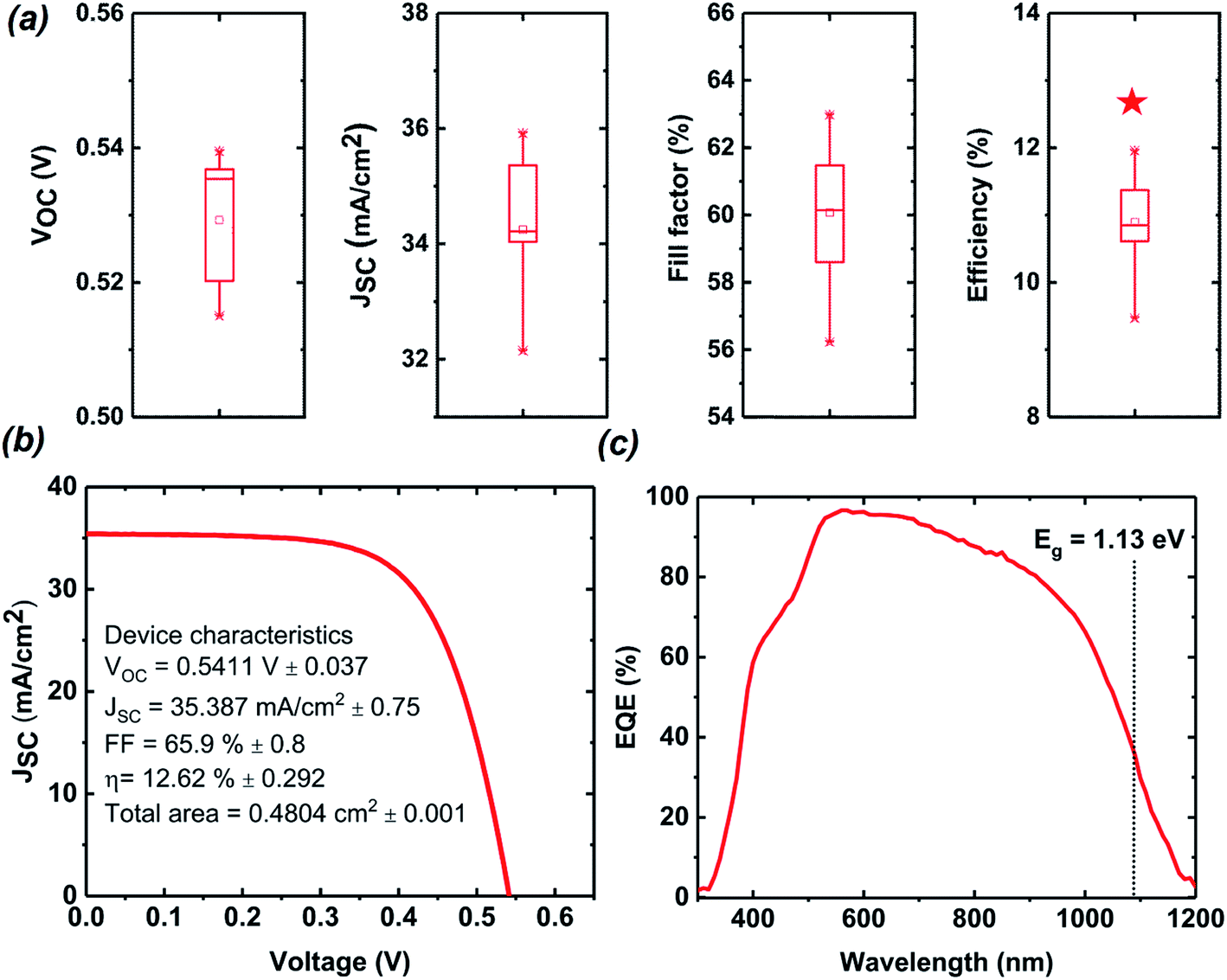 | ||
| Fig. 7 (a) Statistical box charts of in-house measured photovoltaic parameters of 10 cells based on CZTSSe films grown using the Sn/Cu/Zn/Mo/glass structure in the sulfo-selenization process. The red star denotes the efficiency of the champion cell. (b) Certified J–V curve and (c) EQE curve for the highest efficiency CZTSSe device. The maximum in the derivative of the EQE curve in the long-wavelength range is used to estimate the absorber bandgap (see Fig. S8†). | ||
| *VOC [mV] | *JSC [mA/cm−2] | *F·F. [%] | *Efficiency [%] | R s [Ω cm2] | G s [mS cm−2] | A | J 0 [A cm−2] | E g [eV] | E g/q − VOC [V] | |
|---|---|---|---|---|---|---|---|---|---|---|
| DGIST cell | 541.1 | 35.38 | 65.9 | 12.62 | 0.87 | 0.78 | 1.88 | 9.6 × 10⁻⁷ | 1.13 | 0.589 |
| IBM cell | 513.4 | 35.21 | 69.8 | 12.61 | 0.72 | 1.61 | 1.45 | 7.0 × 10⁻⁸ | 1.13 | 0.617 |
To better understand the electrical properties near the CZTSSe/CdS heterojunction, C–V and DLCP measurements were conducted. The C–V and DLCP measurement results in Fig. 8 show carrier density information as a function of depletion width.37 Since DLCP is considered a better measurement method for the bulk carrier density, we can extract the contribution of the interfacial defects by subtracting the bulk density obtained with DLCP from the charge density obtained with C–V measurements. From the DLCP measurements, the depletion width (Xd) can be determined by measuring the capacitance at zero bias, followed by using the formula ε0εA/C, where C is the measured capacitance, A is the device area, ε0 is the vacuum permittivity and ε is the dielectric constant for the absorber. Since the ε of the CZTSSe thin film depends on the bandgap, the value extracted from εr according to the bandgap is used.38ε is approximately 8 for the champion cell. We extracted the carrier density N and Wd estimated from C–V profiling and DLCP. Then, the bulk density (NDLCP), the charge density (NCV) and the depletion width for the champion CZTSSe cell were determined to be ∼1.8 × 1016 cm−3, ∼7.9 × 1016 cm−3 and ∼0.3 μm, respectively. The champion device shows a fairly wide depletion region, but the density (NIT = ∼6.1 × 10¹⁶) of the CTSTSe/CdS interface traps, which is the difference between NCV and NDLCP at zero bias, is high. The high density of traps at the interface is interpreted as evidence of a high recombination rate at the CdS/CZTSSe interface, which has a negative effect on the device characteristics. One reason why our device has a high ideality factor is that bulk defects in CZTSSe thin films may be large, but the trap density at the interfaces is high.
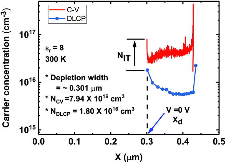 | ||
| Fig. 8 C–V and DLCP characteristics of 12.62% CZTSSe devices at 300 K. The C–V measurement was performed using 50 mV, 100 kHz ac excitation with a dc bias from 0 to −4.5 V, and DLCP was performed using 100 kHz ac excitation with an amplitude from 10 to 100 mV and a dc bias from 0 to −4.5 V. | ||
Using the same approach, we successfully fabricated a large area (1.1761 cm2) CZTSSe cell with a certified efficiency of 11.28% VOC of 533.3 mV, JSC of 33.56 mA cm−2 and F.F. of 63.1% (see Fig. S7-2†). Although the efficiency was lower than the maximum efficiency of a small area cell, a high efficiency of greater than 10% could be realized even with a large area. This efficiency is the highest value for CZTSSe solar cells with an area of ∼1 cm2 or larger, which is the required cell area for inclusion in PIP Table 1.28 The above 2 new records, 12.6% and 11.3%, were included in the recent PIP solar cell efficiency Tables 1 and 2,† respectively.28 The properties of large-area cells will be explained by further studies, such as studies on the subsequent heat treatment uniformity and the effect of heat transfer.
In future studies, fine control of the heat treatment process may be necessary, such as realization of component homogeneity and secondary elimination of the absorber, to further increase the power conversion efficiency.
4. Conclusions
In this work, we fabricated a CZTSSe solar cell with the world′s highest efficiency of 12.62% for a small area cell (0.4804 cm2) and 11.28% for a standard sized cell (1.1761 cm2) using a pure metal SCZM precursor structure and a sulfo-selenization process with H2S gas. The different roles of S, which is a commonly known bandgap control material in CZTSSe thin films, were described in detail. We have presented the Zn volatilization and the mechanism of nanowire formation during the selenization process of pure metal precursors. The H2S gas used in the sulfo-selenization process reacts with Zn before Zn is volatilized to form a ZnSSe thin film. The composition of the absorber layer can be effectively controlled and CZTSSe thin films can be easily produced because of the suppression of the Zn element volatilization by S. These results show the same effect for a S or SeS2 powder source as well as for H2S gas. However, the sulfo-selenization process with H2S gas is more reproducible than that with S or SeS2 powder, and CZTSSe thin films with uniform compositions can be fabricated. Although the CZTSSe thin films fabricated using pure metal precursors showed large void regions and many secondary phases, a high efficiency was obtained. Along with improvements in VOC and JSC, the 12.62% efficiency of the CZTSSe device ties the record achieved in 2013 by IBM. Despite having the same bandgap value as the IBM device, the CZTSSe device shows a low VOC deficit. A key factor in improving the device efficiency is reducing the VOC deficit. Additionally, the relatively low F.F. can be further improved through the control of the buffer and TCO thin film layer thicknesses and through optimized optical design of the top grid. In addition, the optimized p–n junction interface, back contact and absorber with few defects should be further studied to realize higher power conversion efficiencies in the future.Conflicts of interest
There are no conflicts to declare.Acknowledgements
This work was supported by the DGIST R&D Program (19-BD-05) and the Technology Development Program to Solve Climate Changes of the National Research Foundation (2016M1A2A2936781) funded by the Ministry of Science and ICT, Republic of Korea. This work was also supported by the KETEP and the Ministry of Trade, Industry & Energy (No. 20173010012980).References
- Q. Guo, G. M. Ford, W.-C. Yang, B. C. Walker, E. A. Stach, H. W. Hillhouse and R. Agrawal, J. Am. Chem. Soc., 2010, 132, 17384–17386 CrossRef CAS PubMed.
- J. J. Scragg, P. J. Dale, L. M. Peter, G. Zoppi and I. Forbes, Phys. Status Solidi B, 2008, 245, 1772–1778 CrossRef CAS.
- H. Katagiri, K. Saitoh, T. Washio, H. Shinohara, T. Kurumadani and S. Miyajima, Sol. Energy Mater. Sol. Cells, 2001, 65, 141–148 CrossRef CAS.
- D. A. R. Barkhouse, O. Gunawan, T. Gokmen, T. K. Todorov and D. B. Mitzi, Progress in Photovoltaics: Research and Applications, 2012, 20, 6–11 CrossRef CAS.
- H. Katagiri, K. Jimbo, W. S. Maw, K. Oishi, M. Yamazaki, H. Araki and A. Takeuchi, Thin Solid Films, 2009, 517, 2455–2460 CrossRef CAS.
- W. Ki and H. W. Hillhouse, Adv. Energy Mater., 2011, 1, 732–735 CrossRef CAS.
- W. Wang, M. T. Winkler, O. Gunawan, T. Gokmen, T. K. Todorov, Y. Zhu and D. B. Mitzi, Adv. Energy Mater., 2014, 4, 1301465 CrossRef.
- P. D. Antunez, S. Li, D. M. Bishop, D. B. Farmer, T. S. Gershon, J. B. Baxter and R. Haight, Appl. Phys. Lett., 2018, 113, 033903 CrossRef.
- Y.-F. Qi, D.-X. Kou, W.-H. Zhou, Z.-J. Zhou, Q.-W. Tian, Y.-N. Meng, X.-S. Liu, Z.-L. Du and S.-X. Wu, Energy Environ. Sci., 2017, 10, 2401–2410 RSC.
- K.-J. Yang, D.-H. Son, S.-J. Sung, J.-H. Sim, Y.-I. Kim, S.-N. Park, D.-H. Jeon, J. Kim, D.-K. Hwang, C.-W. Jeon, D. Nam, H. Cheong, J.-K. Kang and D.-H. Kim, J. Mater. Chem. A, 2016, 4, 10151–10158 RSC.
- C. Yan, J. Huang, K. Sun, S. Johnston, Y. Zhang, H. Sun, A. Pu, M. He, F. Liu, K. Eder, L. Yang, J. M. Cairney, N. J. Ekins-Daukes, Z. Hameiri, J. A. Stride, S. Chen, M. A. Green and X. Hao, Nat. Energy, 2018, 3, 764–772 CrossRef CAS.
- A. Fairbrother, L. Fourdrinier, X. Fontané, V. Izquierdo-Roca, M. Dimitrievska, A. Pérez-Rodríguez and E. Saucedo, J. Phys. Chem. C, 2014, 118, 17291–17298 CrossRef CAS.
- S. Giraldo, E. Saucedo, M. Neuschitzer, F. Oliva, M. Placidi, X. Alcobé, V. Izquierdo-Roca, S. Kim, H. Tampo, H. Shibata, A. Pérez-Rodríguez and P. Pistor, Energy Environ. Sci., 2018, 11, 582–593 RSC.
- D.-H. Son, D.-H. Kim, S.-N. Park, K.-J. Yang, D. Nam, H. Cheong and J.-K. Kang, Chem. Mater., 2015, 27, 5180–5188 CrossRef CAS.
- G. Zoppi, I. Forbes, R. W. Miles, P. J. Dale, J. J. Scragg and L. M. Peter, Progress in Photovoltaics: Research and Applications, 2009, 17, 315−–319 CrossRef CAS.
- C. M. Fella, A. R. Uhl, Y. E. Romanyuk and A. N. Tiwari, Phys. Status Solidi A, 2012, 209, 1043–1048 CrossRef CAS.
- J. Han, S. Jeon and W. K. Kim, Thin Solid Films, 2013, 546, 321–325 CrossRef CAS.
- A. Weber, R. Mainz and H. W. Schock, J. Appl. Phys., 2010, 107, 013516 CrossRef.
- P. M. P. Salomé, P. A. Fernandes and A. F. da Cunha, Thin Solid Films, 2009, 517, 2531–2534 CrossRef.
- M. G. Gang, S. W. Shin, C. W. Hong, K. V. Gurav, J. Gwak, J. H. Yun, J. Y. Lee and J. H. Kim, Green Chem., 2016, 18, 700–711 RSC.
- F.-I. Lai, J.-F. Yang, Y.-L. Wei and S.-Y. Kuo, Green Chem., 2017, 19, 795–802 RSC.
- K.-J. Yang, J.-H. Sim, D.-H. Son, D.-H. Kim, G. Y. Kim, W. Jo, S. Song, J. Kim, D. Nam, H. Cheong and J.-K. Kang, Progress in Photovoltaics: Research and Applications, 2015, 23(12), 1771–1784 CrossRef CAS.
- H.-P. Zhou, W.-C. Hsu, H.-S. Duan, B. Bob, W. Yang, T.-B. Song, C.-J. Hsu and Y. Yang, Energy Environ. Sci., 2013, 6, 2822–2838 RSC.
- A. Fairbrother, X. Fontané, V. Izquierdo-Roca, M. Espindola-Rodriguez, S. López-Marino, M. Placidi, J. López-García, A. Pérez-Rodríguez and E. Saucedo, ChemPhysChem, 2013, 14, 1836–1843 CrossRef CAS PubMed.
- F. Liu, F. Zeng, N. Song, L. Jiang, Z. Han, Z. Su, C. Yan, X. Wen, X. Hao and Y. Liu, ACS Appl. Mater. Interfaces, 2015, 7, 14376 CrossRef CAS PubMed.
- K. Woo, Y. Kim, W. Yang, K. Kim, I. Kim, Y. Oh, J. Y. Kim and J. Moon, Sci. Rep., 2013, 3, 3069 CrossRef PubMed.
- S.-Y. Kim, D.-H. Son, Y.-I. Kim, S.-H. Kim, S. Kim, K. Ahn, S.-J. Sung, D.-K. Hwang, K.-J. Yang, J.-K. Kang and D.-H. Kim, Nano Energy, 2019, 59, 399–411 CrossRef CAS.
- M. A. Green, Y. Hishikawa, E. D. Dunlop, D. H. Levi, J. Hohl-Ebinger, M. Yoshita and A. W. Y. Ho-Baillie, Progress in Photovoltaics: Research and Applications, 2019, 27, 3–12 CrossRef.
- C.-Y. Chou and S.-W. Chen, Acta Mater., 2006, 54, 2393–2400 CrossRef CAS.
- N. Wang, Y. Cai and R. Q. Zhang, Mater. Sci. Eng. R Rep, 2008, 60, 1–51 CrossRef.
- G.-C. Yi, Semiconductor Nanostructures for Optoelectronic Devices, Springer, Berlin Heidelberg, 2012 Search PubMed.
- J. D. McKinley and J. E. Vance, J. Chem. Phys., 1954, 22, 1120–1124 CrossRef CAS.
- T. Ericson, T. Kubart, J. J. Scragg and C. Platzer-Björkman, Thin Solid Films, 2012, 520, 7093–7099 CrossRef CAS.
- J. J. Scragg, P. J. Dale, D. Colombara and L. M. Peter, ChemPhysChem, 2012, 13, 3035–3046 CrossRef CAS PubMed.
- M. A. Green, Y. Hishikawa, E. D. Dunlop, D. H. Levi, J. Hohl-Ebinger and A. W. Y. Ho-Baillie, Progress in Photovoltaics: Research and Applications, 2018, 26, 3–12 CrossRef.
- E. Lorenzo, Solar Electricity: Engineering of Photovoltaic Systems, Sevilla, Spain, 1994 Search PubMed.
- J. T. Heath, J. D. Cohen and W. N. Shafarman, J. Appl. Phys., 2004, 95, 1000–1010 CrossRef CAS.
- O. Gunawan, T. Gokmen, C. W. Warren, J. D. Cohen, T. K. Todorov, D. A. R. Barkhouse, S. Bag, J. Tang, B. Shin and D. B. Mitzi, Appl. Phys. Lett., 2012, 100(25), 253905 CrossRef.
- P. Nash and A. Nash, ASM Handbook, Alloy phase diagram, ASM International, Materials Park, OH, 1992, vol. 3 Search PubMed.
- S. S. Hegedus and W. N. Shafarman, Progress in Photovoltaics: Research and Applications, 2004, 12, 155–176 CrossRef CAS.
- J. R. Sites and P. H. Mauk, Sol. Cells, 1989, 27, 411–417 CrossRef CAS.
Footnote |
| † Electronic supplementary information (ESI) available. See DOI: 10.1039/c9ta08310c |
| This journal is © The Royal Society of Chemistry 2019 |