
 Open Access Article
 This Open Access Article is licensed under a
 Creative Commons Attribution 3.0 Unported Licence
Plasma assisted vapor solid deposition of Co3O4 tapered nanorods for energy applications†
Mojtaba
Gilzad Kohan
 a,
Raffaello
Mazzaro
ab,
Vittorio
Morandi
b,
Shujie
You
a,
Isabella
Concina
a and
Alberto
Vomiero
*ac
a,
Raffaello
Mazzaro
ab,
Vittorio
Morandi
b,
Shujie
You
a,
Isabella
Concina
a and
Alberto
Vomiero
*ac
aDivision of Materials Science, Department of Engineering Sciences and Mathematics, Luleå University of Technology, 97187 Luleå, Sweden. E-mail: alberto.vomiero@unive.it; alberto.vomiero@ltu.se
bCNR-IMM, Area della Ricerca di Bologna, Via Piero Gobetti 101, 40139, Bologna, Italy
cDepartment of Molecular Sciences and Nanosystems, Ca' Foscari University of Venice, Via Torino 155, 30172 Venezia Mestre, Italy
First published on 2nd October 2019
Abstract
Self-standing, 1-dimensional (1D) structures of p-type metal oxide (MOx) have been the focus of considerable attention, due to their unique properties in energy storage and solar light conversion. However, the practical performance of p-type MOx is intrinsically limited by their interfacial defects and strong charge recombination losses. Single crystalline assembly can significantly reduce recombination at interface and grain boundaries. Here, we present a one-step route based on plasma assisted physical vapor deposition (PVD), for the rational and scalable synthesis of single crystalline 1D vertically aligned Co3O4 tapered nanorods (NRs). The effect of PVD parameters (deposition pressure, temperature and duration) in tuning the morphology, composition and crystalline structure of resultant NRs is investigated. Crystallographic data obtained from X-ray diffraction and high-resolution transmission electron microscopy (TEM) indicated the single crystalline nature of NRs with [111] facet preferred orientation. The NRs present two optical band gaps at about 1.48 eV and 2.1 eV. Current–voltage (I–V) characteristic of the Co3O4 NRs electrodes, 400 nm long, present two times higher current density at −1 V forward bias, compared to the benchmarking thin film counterpart. These array structures exhibit good electrochemical performance in lithium-ion adsorption–desorption processes. Among all, the longest Co3O4 NRs electrodes delivers a 1438.4 F g−1 at current density of 0.5 mA cm−2 and presents 98% capacitance retention after 200 charge–discharge cycles. The very low values of charge transfer resistance (Rct = 5.2 Ω for 400 nm long NRs) of the NRs testifies their high conductivity. Plasma assisted PVD is demonstrated as a facile technique for synthesizing high quality 1D structures of Co3O4, which can be of interest for further development of different desirable 1D systems based on transition MOx.
Introduction
The development of p-type semiconducting metal oxides (MOx), as an alternative to traditional semiconductors (amorphous p-type Si and organic semiconductors) has gained significant attention due to their interesting properties such as tailorable band gap, spanning from UV to visible spectral region, tunable charge transport, light scattering and transparency through feasibly exploiting complex structural networks and morphologies.1Implementing semi-transparent p-type MOx can enable significant improvements in such applications where higher photoelectric efficiency and electronic complexity of circuits are required. Such applications include transparent electronics, photovoltaics and optoelectronics,2 photo detectors, energy storage3 and hydrogen evolution devices.4 Capitalizing on their unique properties to fabricate high performance devices, such as the so-called inverted structures, p-type metal oxides can result in enhanced solar light absorption5,6 and dramatic reduction of back light disruptions, light loss4 and power consumption in the cases of transparent transistors.1
On the other hand, the main obstacles in utilizing p-type MOx, compared to their n-type counter parts, render around their limited intrinsic electronic properties: (i) unlike n-type MOx, the valence band of p-type MOx is low in energy, therefore generated holes can be compensated by formation of native electron donors; (ii) another serious impediment, is their large hole effective mass (mh), mainly resulting from oxygen 2p orbitals in their valence band.7,8 One solution to overcome such fundamental restrictions is to exploit engineered nanostructures and morphologies such as one-dimensional (1D) and/or single crystalline structures,9 which promise unique optoelectronic properties, low threshold lasing10,11 and enhanced carrier mobility.12
One of the p-type MOx semiconductors which has received growing interest as a photoactive material is tricobalt tetraoxide. Co3O4 has been demonstrated to possess great potential as functional material in several applications including, heterogeneous catalysis,7,13 energy storage,3,14 photo-energy conversion and gas sensors14 due to its long-term photostability and strong light absorption in the full visible range (having different energy gaps Eg = 0.74,15 1.5, 2.1 (ref. 16) and 4.4 eV (ref. 15)). On the other hand, the intrinsically poor charge conductivity and low reaction kinetics limit its use in real scenario applications.
A common approach to overcome these problems is by modifying the surface area, particle size, crystalline habit and morphology, which can alter the chemical and physical properties of the material, leading to facet-dependent properties of nanostructures.17 In this sense, different morphologies of Co3O4, such as nanosheets,18,19 nanorods (NRs),20 nanotubes,21,22 nanowalls23 and nanowires (NWs)24–26 with special textures and aspect ratios have been widely exploited.
Among all, 1D nanostructures offer a series of geometrical and structure-related properties, including enhanced light scattering, fast charge transport,9,12 and high diffusion coefficient of ions (Li+), which can limit charge recombination losses and make them more effective in photo-conversion and energy storage devices. In particular, employing Co3O4 as a negative electrode in super capacitors has gained significant attention, due to the long-term stability and high theoretical capacitance (3560 F g−1). However, similar to most transition metal oxides, Co3O4 electrodes suffer adversely from their poor electrical conductivity and capacitance degradation.25,27
Alternatively, recent studies showed that incorporating Co3O4 NRs grown along specific crystallographic directions results in high specific capacitance and fast ions insertion in their structure. For this purpose, significant efforts are directed toward scalable synthesis of 1D systems of Co3O4 through number of methodologies, including hydrothermal method16,17,28 laser ablation17,29 molecular beam epitaxy,30 chemical vapor deposition (CVD)17 and template assisted techniques.6,27,31
Most of the functionalities of 1D Co3O4 nanostructures (for instance the capacitance) considerably varies depending on fabrication method and preparation techniques.27 In addition, there are very few techniques capable to combine the rational production of high quality Co3O4 NRs with controlled shape, size and alignment along with scalable and flexible characteristics that do not entail any peculiar deficiencies in their performance.
In this regard, a key step is the development of a scalable synthetic route, offering tailorable and reproducible properties. Herein, we describe an innovative one-step physical vapor deposition (PVD) to synthesize template free, self-standing single crystal Co3O4 vertically aligned NR arrays on various substrates in a magnetron sputtering configuration at low temperature and with conformal substrate coverage. The control of the sputtering conditions enables creation of Co3O4 vertically aligned NRs arrays through direct vapor solid (VS) condensation, and permits rational one-step fabrication of 1D NRs without any external catalysts, which is endowed in other synthesis routes like CVD, hydrothermal etc. Although, the synthesis of Co3O4 NRs has been already reported, the implemented route in this work grants a facile and highly controllable methodology, not permitted by the other methods. In fact, hydrothermal or sol–gel methods provide low temperature and scalable processes to obtain crystalline structures, but they often result in poor alignment of the 1D structures, which present a high density of structural defects. In addition, previously reported columnar structures of different MOx using PVD are mainly polycrystalline and hard to replicate.32
Experimental
Synthesis of the Co3O4 nanorods
The Co3O4 NR arrays were deposited on single crystal silicon substrates and fluorine-doped tin oxide (FTO) conducting glass (Pilkington TEC15) by means of a reactive DC magnetron sputtering technique using a 99.95% pure cobalt target. The base pressure was in the range of ∼10−7 mPa. The deposition was performed at constant forward power of 70 W on a three-inch target. The target surface temperature during the deposition was altered to ∼200 °C estimated using a thermocouple placed inside the deposition chamber.The sputtering gas was a reactive mixture of argon and 5% oxygen with a gas flow rate of 25 standard cubic centimeters per minute (sccm). On the other hand, the deposition pressure onset was conceived to be an influential factor on the morphology of the deposited Co3O4 electrodes. Irrespective of the introduced reactive gas inside the chamber, the deposition pressure was modified by altering the angle of vacuum outlet hatch in the range from 1.3 × 10⁻³ to 3.2 × 10⁻² mbar. Notably, the increase in deposition pressure yields direct relation to oxidization level of sputtering particles. The substrates were heated at 300 °C during the deposition process, in order to achieve complete oxidization of the depositing cobalt oxide species. We also carried out sputtering reposition at RT, by choosing as deposition parameters the one for the growth of NRs, to investigate the dependence of the oxidation process from the temperature.
Characterization
Scanning electron microscopy (SEM) was carried out using Magellan XHR 400L Field Emission-SEM with 3 kV electron beam voltage. X-ray diffraction patterns were recorded on the PANalytical Empyrean diffractometer using a Cu anode (Kα emission line at 8.04 keV) in the range of 15° < 2θ < 80°. The Raman spectra were recorded in back scattering geometry using a Senterra Raman spectrometer Bruker, equipped with a 50× objective lens to focus the 532 nm excitation laser on the sample and eventually collect the backscattered Raman signal. Rutherford backscattering spectrometry (RBS) was carried out to obtain information about composition and thickness of the samples. A 2.0 MeV 4He+ beam was applied, at backscattering angle Ω = 160° in IBM geometry. Absorption spectra were recorded by means of Agilent cary5000 UV-vis-NIR spectrophotometer from 200 nm to 1100 nm.High resolution-transmission electron microscopy (HR-TEM) analysis was performed on a FEI Tecnai F20 operated at 200 kV. TEM samples were prepared by mechanical removal of the NRs from Si substrate, followed by sonication in isopropanol and drop casting onto carbon-coated Cu TEM grids. The TEM grids were dried for 30 min at RT before analysis. SAED patterns were collected at camera length 490 mm centering the SA aperture on the area covered by a single NRs.
The specific surface area of the samples was evaluated using the Brunauer–Emmett–Teller (BET) plot by nitrogen gas adsorption–desorption isotherm using a Gemini VII instrument.
Current–voltage (I–V) characteristics was analyzed using a ModulabXM (Solartron Analytical) potentiostat, by employing a two-probe setup, in solid-state. During the solid-state measurements in dry conditions, the samples were mounted on a flat holder with one probe attached to the conductive substrate and a spring-legged probe in smooth contact with the surface of Co3O4 NRs film. The I–V curves were recorded in the range of −1 V to 1 V in order to prevent contributions of Joule heating, which may affect the I–V characteristics at higher voltages.
Electrochemical measurements were conducted in a three-electrode cell setup, in 5 M LiCl aqueous solution electrolyte, with a Pt foil (0.6 × 0.6 cm2) as the counter electrode (positive electrode in a capacitor type faradaic device), and an Ag/AgCl as a reference electrode. The electrochemical impedance spectroscopy (EIS) of Co3O4 NRs electrodes were conducted at Co3O4/5 M LiCl (aqueous) interface, after 10 charge–discharge cycles over the frequency range of 1 MHz to 10 mHz with an AC amplitude of 10 mV, since ten charge–discharge cycles is conventionally conceived as suitable set point for formation of solid electrolyte interface (SEI) layer in energy storage applications. All electrochemical data were recorded under ambient atmosphere and at room temperature (RT).
Results and discussion
Schematic illustration of the synthesis of Co3O4 NRs is shown in Fig. 1(a). The governing mechanism for fabricating array structures of Co3O4 NRs is based on low-temperature epitaxial plasma assisted vapor solid (VS) growth of Co3O4 under reactive gas (oxygen) atmosphere. To gain a comprehensive understanding on the mechanism of formation of vertically aligned columnar Co3O4 NRs, we varied the following process parameters: (i) deposition pressure onset and (ii) deposition duration. In a typical synthesis method via VS deposition, the process initializes by evaporation of high-energy nucleus species of target material, followed by subsequent deposition and complete reduction of these species on a substrate. One of the key parameters in the formation of NRs, unlike ordinary films, is the degree of supersaturation (SS). SS is defined as the average partial pressure of initially generated high-energy particles sputtered by the target, and the pressure of the particles in the dark region of plasma column depositing on the substrate after traveling through the plasma.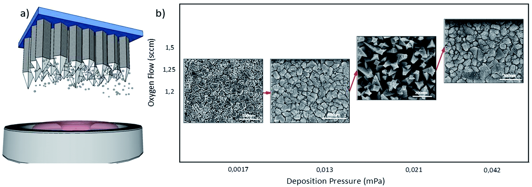 | ||
| Fig. 1 (a) Schematic view of the Co3O4 NRs synthesis via physical vapor deposition. (b) The morphological changes of the deposited Co3O4 films with respect to their deposition pressure onset on FTO substrate. | ||
In the present case, the VS mechanism initiates by formation of highly thermalized oxidized particles at the surface of the plasma ignited target due to target heating and ion bombardment of Ar/O2 gas.33 The generation of highly thermalized particles is in the present case achieved by adjusting the deposition pressure. Enhancement of deposition pressure in an Ar/O2 gas environment results in the formation of highly oxidized particles. At the same time, it lowers the average kinetic energy of the impinging Ar+ ions on the surface of the target.33 The lower average energy of Ar+ ions induces lower density (and kinetic energy) of sputtered particles and lower SS degree, which is suitable for the growth of NRs arrays through the VS mechanism.34,35 Finally, the intermediate thermalized vapors spontaneously condense and recrystallize on the surface of the substrate as a result of Gibbs energy reduction. Considering their SS degree, the condensed vapors can converge toward a NR like structure, by assembling the high energy vapor particles on top of each other, toward the direction of their lowest energy facet, functioning as building blocks for the NRs.
The variation of the deposition pressure alters the degree of SS, modifying substantially the shape of the deposited nanostructures. A clear evidence is given in Fig. 1(b). The deposition pressure of 1.6 × 10⁻² mPa attains to fabrication of 1D NRs arrays of Co3O4. High deposition pressure of 4.2 × 10⁻² mPa leads to formation of a randomly structured, coarse film (Fig. S3(d)†). Higher deposition pressure results in lower deposition rate and very thin films, due to excessive inter-collision of sputtering ions in the chamber.33 Lower deposition pressure resulted in formation of compacted cubic structure and ordinary Co3O4 films (Fig. 1(b)). Specifically, the texture of the films can be tuned by the variation of SS degree ensuing a different architecture of sputtered building blocks. The effect of deposition pressure on morphology of deposited Co3O4 films is further depicted in Fig. S3 (ESI†).
A closer look to samples exhibiting NR shape is reported in Fig. 2(a)–(d). Cross sectional and planar SEM images of the as grown Co3O4 NRs on silicon substrate indicate uniform and conformal substrate coverage from 1D tapered Co3O4 NRs, with regular square cross section, and with areal density of ∼150 NRs per μm2 through the entire surface of the substrates. The average lateral size of the NRs on Si is (53 ± 7) nm for 60 min deposition, measured from SEM images. Deposition on FTO does not modify significantly the lateral size of the NRs (55 ± 10) nm for the same deposition time (see Fig. S1(c) and (d)†). The cross section SEM image in Fig. 2(b) shows the direct uniform growth of the Co3O4 NRs from the substrate, which eventually leads to a fine pyramid shape at the ending tip. The mean longitudinal length of the Co3O4 NRs (for both Si and FTO substrates) is about 700 nm, pertinent to a sputter deposition time of 60 minutes on silicon substrates.
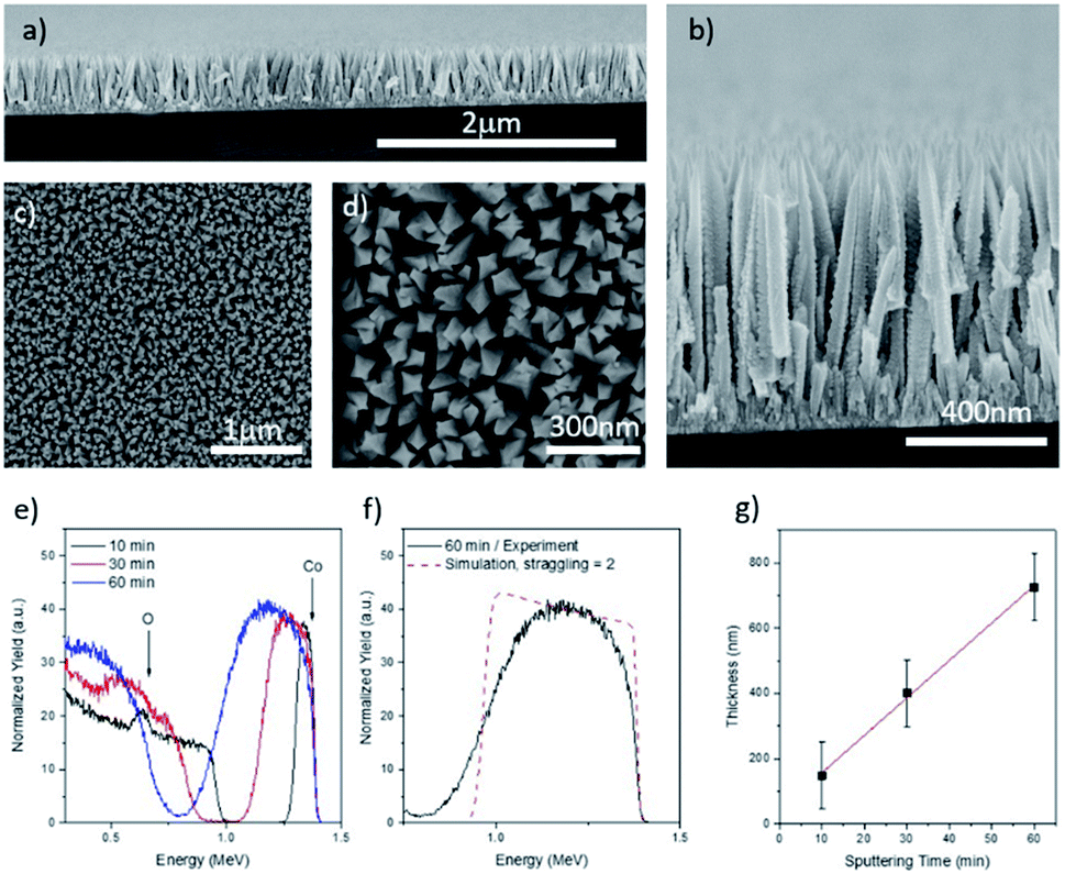 | ||
| Fig. 2 (a and b) Cross section view of the Co3O4 NRs on silicon substrate. (c and d) Planar view of the Co3O4 vertically aligned NR arrays presenting high surface roughness and conformal dense coverage of the substrates. (e) Experimental RBS spectra of Co3O4 NRs substrates with different deposition durations. (f) Experimental and simulated RBS spectrum for Co3O4 NRs electrode under 60 min sputter deposition. (g) Co3O4 NRs thickness versus deposition duration, obtained from RBS results. | ||
RBS spectra for 10, 30 and 60 min sputter deposition on Si substrate are reported in Fig. 2(e)–(g), respectively. The films exhibit a stoichiometric composition equal to Co3O3.0±0.5, with slight oxygen deficiency, with respect to the nominal Co3O4 composition. No spurious contaminants are detected. As expected, the thickness of the deposited layers increases linearly with the deposition time (Fig. 2(g)). The most noticeable feature of RBS spectra relates to the broadening of the signal in both the front and backside, as highlighted in Fig. 2(f), where the region related to Co signal is reported. The RUMP code simulation (dashed red line) is overlapped to the experimental spectrum, to highlight peak broadening. Such broadening is not compatible with the standard broadening due to straggling effect36 and is a clear indication that the grown layer features a very rough surface, compatible with a NR morphology (as clearly demonstrated by SEM and TEM). Fig. 3(a) shows the X-ray diffraction pattern for Co3O4 films with different morphologies, synthesized at different pressure on FTO glass. All the samples present reflection peaks at 2θ values of 18.91°, 31.27° and 36.75°, attributed to (111), (022) and (311) facets of spinel crystalline structure. Accordingly, there is no evidence of complex and second phases of Co3O4, which is typically formed in other synthesis methods, like the hydrothermal one.37
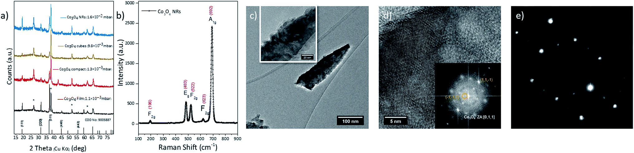 | ||
| Fig. 3 (a) Evolution of X-ray diffraction pattern of the different produced Co3O4 morphologies on FTO substrate. The peaks labeled with the asterisk are coming from the FTO substrate. (b) Raman spectrum recorded for Co3O4 NRs. (c) Low magnification TEM micrograph of a nanorod deposited on carbon-coated grid. (Inset) Detail of the NRs morphology, displaying the high roughness surface. (d) HR-TEM micrograph of the same NRs displaying a single crystal domain and (inset) relative FFT. (e) Selected area diffraction performed on the same NRs showing a single pattern compatible with Co3O4 with zone axis [0,1,1]. | ||
The sharp characteristic of the peaks is also evidence of the high crystallinity of the nanostructures, which is further confirmed by TEM. The diffraction pattern of polycrystalline Co3O4 film (black line) presented the highest intensity of the (311) peak, typical of Co3O4 spinel phase, compared to other morphologies. Remarkably, moving on from collected XRD pattern of Co3O4 film (black line) toward Co3O4 NRs (blue line), a significant quenching between the intensity ratios of the I(311)/I(111) peaks from (5![[thin space (1/6-em)]](https://www.rsc.org/images/entities/char_2009.gif) :2) to (1:1) is observed. The ratios confirm dominant growth direction of NRs mainly along the [111] crystalline orientation. These findings are in agreement with the SEM and TEM observations. Interestingly the [111] crystalline orientation is reported to have superior effect on the electrochemical performance of Co3O4 NRs in a series of applications.38,39
:2) to (1:1) is observed. The ratios confirm dominant growth direction of NRs mainly along the [111] crystalline orientation. These findings are in agreement with the SEM and TEM observations. Interestingly the [111] crystalline orientation is reported to have superior effect on the electrochemical performance of Co3O4 NRs in a series of applications.38,39
The Raman spectra of the Co3O4 NRs (Fig. 3(b)) confirmed the highly crystalline nature of the synthesized NRs. No mixed phase impurity signal was indeed detected in the Raman spectra. The Raman peaks at 196, 483, 522, 623 and 692 cm−1 are attributed to F2g, Eg, F2g, F2g, and A1g vibrational modes typical of Co3O4 cubic spinel phase. In general, the A1g peak is assigned to the vibrational mode in octahedral sites of spinel cobalt oxide, Eg and F2g modes are corresponding to the mix vibrations of oxygen bonded sites.40
Cross-sectional HR-TEM (Fig. 3(c) and S2†) shows the high surface roughness featured by the NRs, confirming what observed in SEM and RBS analyses. The high crystallinity of the 1D nanostructures is confirmed by FFT analysis, reported in Fig. 3(d), which also indicates the presence of a single phase compatible with Co3O4 crystal lattice (Fig. 3(d), zone axis [011]). The (111) fringes are also noticed along the main NR axis, consistent with XRD analysis. The NRs exhibit single crystal structure along the whole 1D structure, as confirmed by the Selected Area Diffraction performed on the entire nanowire, shown in Fig. 3(e).
The optical properties of the Co3O4 NRs were investigated by means of UV-vis-NIR spectroscopy. The transmittance spectrum of the Co3O4 NRs is reported in Fig. 4. The material features high absorption of light in the visible region with two noticeable drops centered at 450 nm and 730 nm, which can be assigned to the O2− → Co2+ and O2− → Co3+ electronic transitions, respectively.13,15
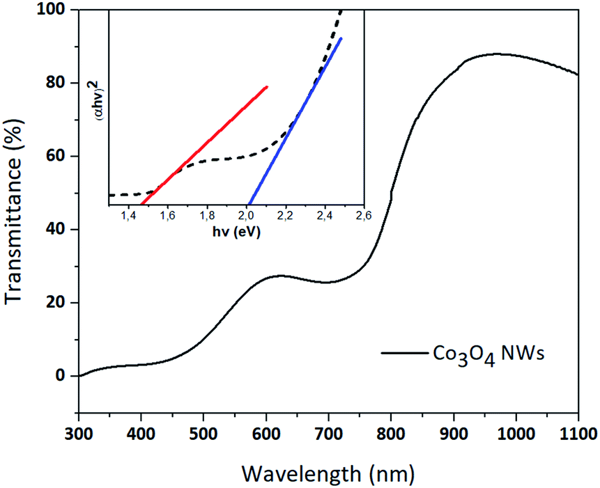 | ||
| Fig. 4 Transmittance spectra of the Co3O4 NRs grown on glass substrate, 400 nm long. (Inset) Band gap measurement of Co3O4 nanorods using Tauc plot method. | ||
The band gap energy (Eg) of the material can be evaluated using Tauc plot method as reported in the inset of Fig. 4. In general, Tauc plot is derived from the following equation:
| (αhν)2 = k(hν − Eg) | (1) |
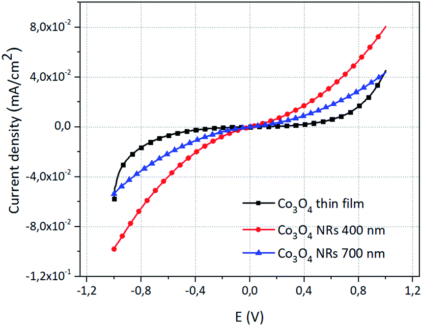 | ||
| Fig. 5 Typical I–V characteristic of the synthesized Co3O4 nanorods with different lengths compared with normal PVD deposited Co3O4 thin film (nominal thickness 600 nm). | ||
BET specific surface area of the Co3O4 NR samples, as deposited on silicon substrate, is measured using adsorption and desorption of N2 gas (Fig. 6(a)). The contribution of the substrate weight (silicon wafer), is removed by measuring the BET surface area of identical silicon substrate and disregarding its specific mass. The surface area of the 700 nm long NRs sample is calculated as 5.3 m2 g−1. Notably, relating the surface area to the areal deposition geometry, for the samples with length of 700 nm, every 1 cm2 of the sample results to a surface area of 176.2 cm2 and mass loading of 1 mg cm−2. The electrochemical properties of Co3O4 NR electrodes are investigated using cyclic voltammetry (CV) EIS. An aqueous solution of LiCl is provided as electrolyte to examine the pseudo-capacitance performance of electrodes in the merits of Li+ ion charge storage ability. CV curves are recorded in a three-electrode setup at different scanning rates. Fig. 6(b) shows the cyclic voltammograms of three Co3O4 electrodes featuring 200, 400 and 700 nm lengths. According to most of the literature in the field, the behavior observed herein should be defined pseudocapacitive, although the matter is controversial.41 The total charge Q involved in the process shows a non trivial behavior in relation to the length of the NRs: it is rather similar as for the electrodes featuring 200 and 400 nm length (Q200nm = 9.5 × 10⁻⁵ mC; Q400nm = 6.61 × 10⁻⁵ mC), while it is greatly, but not linearly, enhanced when the NR length reaches 700 nm (Q700nm = 2.29 × 10⁻⁴ mC).
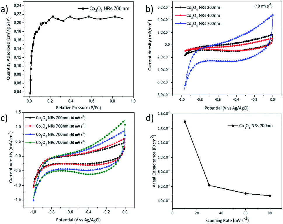 | ||
| Fig. 6 (a) Isotherm linear plot of N2 adsorption–desorption of the 700 nm Co3O4 NRs sample. (b) CV curves collected for three different lengths of Co3O4 NR electrodes at scan rate of 10 mV s−1. (c) Recorded CV data for Co3O4 700 nm sample with different scanning rates. (d) Variation of areal capacitance versus scanning rate. | ||
Similar, to previous studies, the CV trends in potential window between −0.9 to 0 V presented a tail of reversible faradaic current ending at −0.9 V. The reversible faradaic current can be assigned to charge transfer process of the electro-adsorbed ions of electrolyte on the Co3O4 electrodes resulting from drastic formation of SEI layer, which can be assigned to the high surface area in contact with electrolyte.42,43
Notably, electrodes with longer NRs, and enhanced electrochemical surface area, presented higher areal capacitance values, which can correspond to higher loading of diffused ions. The specific capacitance values for different electrodes are presented in Table 1. The CV profile for the electrode with the highest capacitance value (Co3O4 NRs electrode, 700 nm long) is recorded at different scanning rates (Fig. 6(c)). All the CV curves exhibited the same shape plateau in different voltage sweep rates. Moreover, increasing the CV acquisition rate infers to a lower value of areal capacitance as shown in Fig. 6(d).
| Sample | Areal capacitance (F cm2) |
|---|---|
| Co3O4 NRs 700 nm | 1.5 × 10⁻² |
| Co3O4 NRs 400 nm | 5 × 10⁻³ |
| Co3O4 NRs 200 nm | 3 × 10⁻³ |
The galvanostatic charge–discharge profiles of the 700 nm Co3O4 NRs electrode and a PVD deposited Co3O4 film in the potential range 0 to −0.9 V and current density of 0.1 mA cm−2 are exhibited in Fig. 7(a). The 700 nm Co3O4 NR electrode presented slower discharge plateau than the film electrode, confirming higher capacitance of the crystalline NR structure. The obtained areal capacitance values for the 700 nm Co3O4 NR electrode, are in line with CV data (1.1 × 10⁻² F cm−2 for 0.1 mA cm−2) and indicated ∼16 times higher areal capacitance than the Co3O4 PVD film.
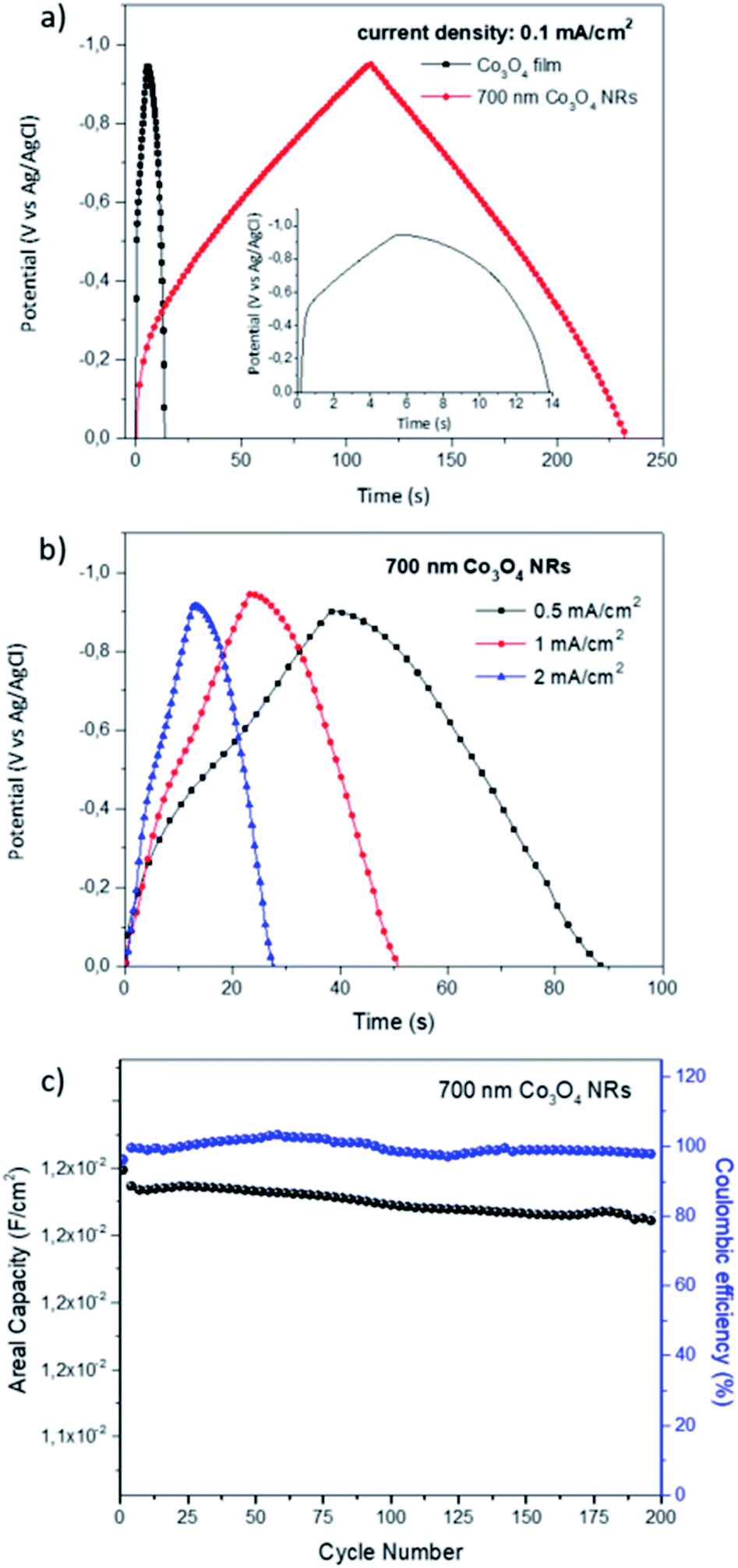 | ||
| Fig. 7 (a) Charge–discharge profile of 700 nm Co3O4 NRs and a PVD deposited film (nominal thickness 400 nm). (b) Charge–discharge behavior of 700 nm electrode under different current densities. (c) Cyclic performance for 200 cycles at 0.1 mA cm−2. | ||
The galvanostatic charge–discharge curves of the 700 nm Co3O4 NR electrode, as a prime candidate for the best electrode performance, under different current densities are presented in Fig. 7(b). Remarkably, all the curves indicated similar non-linear pseudo-capacitance behavior with relatively high discharge rate. The 700 nm Co3O4 NR electrode, exhibits average specific capacitance of 1438.4 F g−1, 1119,7 F g−1 and 819.8 F g−1 at current densities of 0.5 mA cm−2, 1 mA cm−2 and 2 mA cm−2, respectively.
The merely symmetrical charge and discharge trend of the curves can significantly contribute to enhanced reversibility and coulombic efficiency. Remarkably, the storage properties of the electrodes present comparable results to previously reported works indicating a high potential of synthesized Co3O4 NRs via plasma assisted PVD.25,44–46
To investigate the long-term capacitance retention and stability of the electrodes, the galvanostatic charge–discharge measurements are carried out at current density of 0.1 mA cm−2 for 200 cycles. The first 10 cycles show an abrupt capacity decay of nearly 0.5% ascribed to formation of SEI layer and preliminary adsorption of Li+ ions in the bulk of the electrodes.47
Overall stability profile of the sample presented ∼98% capacity retention and a deliverable capacitance of 1.2 × 10⁻² F cm−2 over 200 cycles. The morphology changes of the Co3O4 NRs after 200 cycles, is shown in Fig. S4.† The SEM images demonstrate the overall integrity of the Co3O4 NR electrodes after 200 cycle stability measurements.
The overall capacitive response of the Co3O4 electrodes can be attributed to two main components: the pseudo-capacitance due to surface ions charge transfer (Cps) and the static double-layer capacitance (Cdl) resulting from diffusion charges. To further investigate the contribution of the double-layer capacitance, EIS analysis was carried out on all electrodes with different NR lengths. EIS data are presented in form of Nyquist plot in Fig. 8(a) where Z′′ and Z′ are the imaginary and real parts of impedance, respectively. As mentioned in the Experimental section, the EIS of Co3O4 NRs electrodes were conducted after 10 charge–discharge cycles, which is conventionally conceived as suitable set point for formation of SEI layer in energy storage applications. The diameter of the semicircle at high frequency region corresponds to the charge transfer resistance (Rct) at the SEI and the slope of linear region (Warburg) represents the diffusion of ions (Li+) in the electrodes at lower frequencies. The values for double layer capacitance are measured using the equivalent circuit (inset of Fig. 8(a)) without any specific fitting and are presented in Table 2.
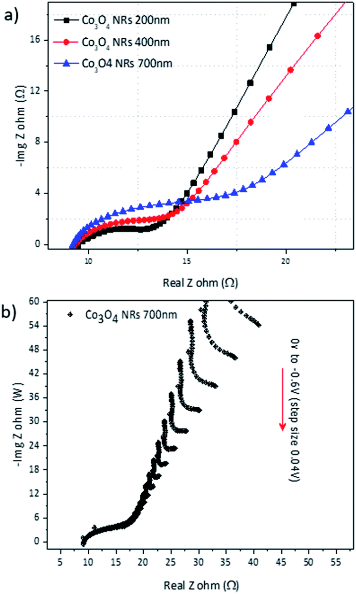 | ||
| Fig. 8 (a) Nyquist plots of Co3O4 electrodes (−Z′′ vs. Z′) recorded after 10 ion diffusion cycles. (b) Series of impedance plots with different polarization potential ranging from −0.6 to 0 V. | ||
| Sample | C dl (F) | R ct (Ω) | Warburg coefficient (Ω) |
|---|---|---|---|
| Co3O4 NRs 700 nm | 1.01 × 10⁻⁶ | 8.8 | 368.7 |
| Co3O4 NRs 400 nm | 7.3 × 10⁻⁷ | 5.2 | 282.8 |
| Co3O4 NRs 200 nm | 4.1 × 10⁻⁷ | 3.2 | 262.5 |
All three electrodes presented very low values of Rct (8.8 Ω for 700 nm Co3O4 electrode), which is in qualitative agreement with the obtained I–V characteristic of the NRs.
The values of charge transfer resistance (Rct) indicated a direct enhancement by the increase in surface area of Co3O4 electrodes or more clearly by enhancement of Co3O4 NRs length. Among these electrodes, the Co3O4 NRs with the longest length (700 nm) offer almost 63% higher Cdl compared to the Co3O4 400 nm electrode, which suggests the positive influence of electrode surface area in the capacitance behavior. In general, the very low impedance values can be attributed to the high crystalline nature of the electrodes. However, the effect of oxygen vacancies, suggested by oxygen deficiency from RBS analysis, can influence the electrochemical performance of electrodes by reducing the impedance values and introducing electro-active sites.48
On the other hand, the solid-state diffusion of Li+ ions, pertaining to the impedance of Warburg region with horizontal axis (Z′), was slightly decreased with increasing the surface area of electrodes (longer Co3O4 NRs), suggesting the slower diffusion of ions in the bulk of electrodes, which yet again indicates that rough nature of the electrodes plays a vital role along this direction. In that sense, the capacitive behavior of NRs is greatly influenced by their surface area as opposed to their length-related impedance demonstrated in Fig. 8(a). It should be considered that the embodiment of the 1D NRs in electrolyte could also provide more active material for Li+ ion transfer that hinders their impedance effect.
Nyquist plots of the Co3O4 700 nm sample with different DC polarization potentials are shown in Fig. 8(b). The data is recorded by changing the DC polarization potential by a step of 0.04 V starting from 0 V and sweeping the frequency over the same range. The semicircle features of the curves indicate a decrease of charge transfer resistance (Rct) for about 88% by lowering the potential onset from −0.6 to 0 V. Conversely, the obtained values of Cdl exhibits a negligible increase (∼7%) at both ends of the DC potential onset (−0.6 to 0 V) implying that the pseudo-capacitance is the main determining parameter in total amount of capacitance compared to Cdl.
Conclusions
This study introduced plasma assisted PVD method as a pioneer synthesis route for high quality fabrication of 1D structures of Co3O4 NRs, a transition p-type MOx semiconductor, with controlled morphology and composition. We assessed the flexibility of this technique for significant modification of the deposited nanostructures by altering relevant parameters such as deposition pressure onset and deposition duration. Morphological characterizations clearly indicated a conformal coverage and highly aligned NR forest arrays of Co3O4 over different substrates. Crystallographic data indicate the high crystalline nature of the NRs and their unique preferred orientation along their [111] facet.The obtained structures demonstrated significant light harvesting properties in the vis-NIR region and the expected optical band gaps. Moreover, the charge transfer properties of the Co3O4 NRs indicated higher current density compared to the thin film counterparts.
In addition, these array structures presented suitable electrochemical performance in lithium-ion adsorption–desorption processes. We correlated the length/lateral side of the NRs with their pseudo-capacitive behavior and the EIS characteristics.
This study demonstrates that the proposed synthetic approach has great potential for the synthesis of different transition MOx, applicable in different energy related frontiers.
Conflicts of interest
The authors claim no conflicts of interests.Acknowledgements
The authors acknowledge Knut & Alice Wallenberg Foundation, the Swedish Foundations Consolidator Fellowship, LTU Lab-fund program and Kempe Foundation for partial funding and The European Union's Horizon 2020 research and innovation programme under grant agreement No. 654002. I. C. acknowledges VINNOVA under the VINNMER Marie Curie Incoming Grant for partial funding (project ‘‘Light Energy”, LiEn, 2015-01513). V. M. and R. M. gratefully acknowledge the European Union's Horizon 2020 research and innovation program under GrapheneCore2 785219 – Graphene Flagship for partial funding.References
- E. Fortunato and R. Martins, Phys. Status Solidi RRL, 2011, 5, 336–339 CrossRef CAS.
- W. Y. Li, L. N. Xu and J. Chen, Adv. Funct. Mater., 2005, 15, 851–857 CrossRef CAS.
- T. Zhu, J. S. Chen and X. W. Lou, J. Mater. Chem., 2010, 20, 7015–7020 RSC.
- I. Concina, Z. H. Ibupoto and A. Vomiero, Adv. Energy Mater., 2017, 1700706, 1700706 CrossRef.
- S. K. Park, T.-H. Kim, J. Heo, Y.-H. Kim, Y. Noh, S. Park, G. Yi, J. Kim, M. Yoon and M. S. Oh, Nature, 2012, 489, 128–132 CrossRef PubMed.
- X. Feng, L. Zhi, U. Kolb, E. Mugnaioli, K. Müllen, Y. Liang and M. G. Schwab, J. Am. Chem. Soc., 2010, 132, 15030–15037 CrossRef PubMed.
- H. Raebiger, S. Lany and A. Zunger, Phys. Rev. B: Condens. Matter Mater. Phys., 2007, 76, 045209 CrossRef.
- R. B. Galland, Am. J. Surg., 2005, 190, 314–318 CrossRef CAS PubMed.
- X. Liu, C. Li, S. Han, J. Han and C. Zhou, Appl. Phys. Lett., 2003, 82, 1950–1952 CrossRef CAS.
- S. Gradečak, F. Qian, Y. Li, H. G. Park and C. M. Lieber, Appl. Phys. Lett., 2005, 87, 1–3 CrossRef.
- S. S. Mao, Int. J. Nanotechnol., 2004, 1, 42 CrossRef CAS.
- W. Lu, J. Xiang, B. P. Timko, Y. Wu and C. M. Lieber, Proc. Natl. Acad. Sci. U. S. A., 2005, 102, 10046–10051 CrossRef CAS PubMed.
- J. A. Koza, Z. He, A. S. Miller and J. A. Switzer, Chem. Mater., 2012, 24, 3567–3573 CrossRef CAS.
- W. Y. Li, L. N. Xu and J. Chen, Adv. Funct. Mater., 2005, 15, 851–857 CrossRef CAS.
- L. Qiao, H. Y. Xiao, H. M. Meyer, J. N. Sun, C. M. Rouleau, A. A. Puretzky, D. B. Geohegan, I. N. Ivanov, M. Yoon, W. J. Weber and M. D. Biegalski, J. Mater. Chem. C, 2013, 1, 4628–4633 RSC.
- X. Xie, Y. Li, Z.-Q. Liu, M. Haruta and W. Shen, Nature, 2009, 458, 746–749 CrossRef CAS PubMed.
- R. J. Kennedy, IEEE Trans. Magn., 1995, 31, 3829–3831 CrossRef CAS.
- J. Liu and X. W. Liu, Adv. Mater., 2012, 24, 4097–4111 CrossRef CAS PubMed.
- F. Faisal, M. Bertram, C. Stumm, S. Cherevko, S. Geiger, O. Kasian, Y. Lykhach, O. Lytken, K. J. J. Mayrhofer, O. Brummel and J. Libuda, J. Phys. Chem. C, 2018, 122, 7236–7248 CrossRef CAS.
- R. Liu, CrystEngComm, 2015, 17, 4449–4454 RSC.
- Q. Zhang, X. Fu, Q. Kan and J. Guan, Ind. Eng. Chem. Res., 2019, 58, 4774–4779 CrossRef CAS.
- C. Niu, J. Meng, X. Wang, C. Han, M. Yan, K. Zhao, X. Xu, W. Ren, Y. Zhao, L. Xu, Q. Zhang, D. Zhao and L. Mai, Nat. Commun., 2015, 6, 1–9 Search PubMed.
- L. Xiong, Y. Teng, Y. Wu, J. Wang and Z. He, Ceram. Int., 2014, 40, 15561–15568 CrossRef CAS.
- K. M. Shaju, F. Jiao, A. Debart and P. G. Bruce, Phys. Chem. Chem. Phys., 2007, 9, 1837–1842 RSC.
- X. Zhang, Y. Zhao and C. Xu, Nanoscale, 2014, 6, 3638–3646 RSC.
- L. Chen, J. Hu, R. Richards, S. Prikhodko and S. Kodambaka, Nanoscale, 2010, 2, 1657 RSC.
- L. Cui, J. Li and X.-G. Zhang, J. Appl. Electrochem., 2009, 39, 1871–1876 CrossRef CAS.
- B. Niu, L. Man and J. Wang, Integr. Ferroelectr., 2011, 129, 181–187 CrossRef CAS.
- J. D. Blakemore, H. B. Gray, J. R. Winkler and A. M. Müller, ACS Catal., 2013, 3, 2497–2500 CrossRef CAS.
- C. A. F. Vaz, D. Prabhakaran, E. I. Altman and V. E. Henrich, Phys. Rev. B: Condens. Matter Mater. Phys., 2009, 80, 1–7 CrossRef.
- H. Tüysüz, Y. J. Hwang, S. B. Khan, A. M. Asiri and P. Yang, Nano Res., 2013, 6, 47–54 CrossRef.
- R. Alvarez, P. Romero-Gomez, J. Gil-Rostra, J. Cotrino, F. Yubero, A. Palmero and A. R. Gonzalez-Elipe, J. Appl. Phys., 2010, 108, 064316 CrossRef.
- R. F. Bunshah, Handb. Hard Coatings Depos. Technol. Prop. Appl., 2001 Search PubMed.
- A. Vomiero, E. Boscolo Marchi, G. Mariotto, G. Della Mea, A. Scandurra and O. Puglisi, J. Appl. Phys., 2005, 97, 034905 CrossRef.
- A. Vomiero, E. B. Marchi, G. Mariotto, A. Quaranta, G. Della Mea, G. Ottaviani, R. Tonini, M. Butturi and G. Martinelli, Appl. Phys. Lett., 2006, 88, 1–3 CrossRef.
- J. W. Mayer and M.-A. N. Wei-Kan Chu, in Backscattering Spectrometry, ed. W.-K. Chu, J. W. Mayer and M.-A. Nicolet, Elsevier, 1978, pp. 323–327 Search PubMed.
- M. V. Reddy, G. Prithvi, K. P. Loh and B. V. R. Chowdari, ACS Appl. Mater. Interfaces, 2014, 6, 680–690 CrossRef CAS PubMed.
- D. Liu, X. Wang, X. Wang, W. Tian, Y. Bando and D. Golberg, Sci. Rep., 2013, 3, 2543 CrossRef PubMed.
- X. Xiao, X. Liu, H. Zhao, D. Chen, F. Liu, J. Xiang, Z. Hu and Y. Li, Adv. Mater., 2012, 24, 5762–5766 CrossRef CAS PubMed.
- V. G. Hadjiev, M. N. Iliev and I. V. Vergilov, J. Phys. C: Solid State Phys., 1988, 21, L199–L201 CrossRef.
- T. Brousse, D. Bélanger and J. W. Long, J. Electrochem. Soc., 2015, 162, A5185–A5189 CrossRef CAS.
- V. Augustyn, P. Simon and B. Dunn, Energy Environ. Sci., 2014, 7, 1597 RSC.
- L. Kong, C. Zhang, J. Wang, W. Qiao, L. Ling and D. Long, Sci. Rep., 2016, 6, 21177 CrossRef CAS PubMed.
- D. Yan, H. Zhang, L. Chen, G. Zhu, S. Li, H. Xu and A. Yu, ACS Appl. Mater. Interfaces, 2014, 6, 15632–15637 CrossRef CAS PubMed.
- J. Sun, C. Wu, X. Sun, H. Hu, C. Zhi, L. Hou and C. Yuan, J. Mater. Chem. A, 2017, 5, 9443–9464 RSC.
- P. Zhang, B. Y. Guan, L. Yu and X. W. D. Lou, Angew. Chem., Int. Ed., 2017, 56, 7141–7145 CrossRef CAS PubMed.
- Y. Lu, L. Yu, M. Wu, Y. Wang and X. W. D. Lou, Adv. Mater., 2018, 30, 4–9 Search PubMed.
- J. Hao, S. Peng, H. Li, S. Dang, T. Qin, Y. Wen, J. Huang, F. Ma, D. Gao, F. Li and G. Cao, J. Mater. Chem. A, 2018, 6, 16094–16100 RSC.
Footnote |
| † Electronic supplementary information (ESI) available. See DOI: 10.1039/c9ta08055d |
| This journal is © The Royal Society of Chemistry 2019 |