
Electron trapping and extraction kinetics on carrier diffusion in metal halide perovskite thin films†
Gyeongho
Kang‡
a,
Jun-Sik
Yoon‡
b,
Guan-Woo
Kim
a,
Kyoungwon
Choi
 a,
Taiho
Park
*a,
Rock-Hyun
Baek
*c and
Jongchul
Lim
*d
a,
Taiho
Park
*a,
Rock-Hyun
Baek
*c and
Jongchul
Lim
*d
aDepartment of Chemical Engineering, Pohang University of Science and Technology, 77 Cheongam-Ro, Nam-Gu, Pohang, Gyeongbuk 37673, Korea. E-mail: taihopark@postech.ac.kr
bInformation Research Laboratories, Pohang University of Science and Technology, 77 Cheongam-Ro, Nam-Gu, Pohang, Gyeongbuk 37673, Korea
cElectrical Engineering, Pohang University of Science and Technology, 77 Cheongam-Ro, Nam-Gu, Pohang, Gyeongbuk 37673, Korea
dClarendon Laboratory, University of Oxford, Parks Road, Oxford OX1 3PU, UK. E-mail: jongchul.lim@physics.ox.ac.uk
First published on 9th September 2019
Abstract
Understanding initial electron distribution, diffusion, trapping and extraction processes for charge transfer kinetics in metal halide perovskite thin films is crucial for the improvement in device performances, but it still remains ambiguous in the research community. In particular, the kinetics of early-time carrier trapping should be considered with that of diffusion because these processes competitively occur in the same time domain. We herein presented the role of free electron trapping for the diffusion process by employing a dynamic trapping model on time-resolved photoluminescence, the most commonly employed technique to investigate charge transfer kinetics. The origin of the stretched exponential decay behavior of the trapping process, which appeared in the fast component of TRPL, was phenomenologically described and further clarified through a simulation study. We found that the electron injection coefficient at the interface between the perovskite and the electron transport layer was a more important determinant than the electron mobility of the perovskite in the electron extraction process.
Introduction
Time-resolved photoluminescence (TRPL) spectroscopy is a simple and distinct analysis method for investigating charge extraction processes.1–8 By applying a charge quencher, such as an electron transport layer (ETL) or a hole transport layer, on the perovskite layer, we can study the charge extraction process from the photoluminescence (PL) decay curve or transient conductivity change.9–14 This experiment has been called surface quenching (SQ)-TRPL.15 However, there are irregular and unclear interpretations for analysing the PL decay curves for the perovskite, which is an elucidation of the bi-exponential-like behaviour in TRPL and SQ-TRPL.16–23 Furthermore, the influence of charge diffusion by initial charge distribution on the trapping process is considered. When light passes through a material, charges are generated throughout the material following the equation G = N0e−αx, where N0 is the photon flux at the surface, α is the absorption coefficient, and x is the light penetration depth into the material (Fig. S1†). There is an exponential charge distribution in the initial stage, followed by the flattening of the charge gradient throughout the entire perovskite layer, which we need to consider when analysing the charge carrier diffusion in transient spectroscopy. Hence, considering the charge carrier diffusion becomes more important when the first-order monomolecular recombination (Shockley–Read–Hall, SRH) occurs in a faster or comparable time domain to that of the diffusion process.24,25 In SRH recombination, the rate of electron capture (Rcn) is written in the form26| Rcn = CnNt[1 − f(Et)]n | (1) |
In this study, we elucidated that charge carrier diffusion is influenced by the competition between electron trapping and extraction processes with different initial electron distributions via time-resolved photoluminescence measurements. For this study, we developed a dynamic trapping model that explained the relationship between charge carrier trapping and diffusion processes in transient spectroscopy. After applying a computational simulation to our experimental data, we found that the electron mobility could influence the kinetics of the dynamic trapping process in carrier diffusion. Notably, using the electron extraction layer at the opposite side of light illumination on perovskites with different thicknesses, we revealed that the electron injection rate at the interface has a significant role in the extraction process than electron diffusion through the perovskite layer. This study can support the understanding of the optoelectronic properties of a material and its various device performances.
Results and discussion
Charge carrier trapping and diffusion processes
All perovskite films discussed here were prepared by a solvent engineering procedure with a composition of Cs0.05(MA0.17FA0.83)0.95Pb(I0.83Br0.17)3.27 The absorption coefficient of the perovskite film was 1.6 × 105 cm−1 at a wavelength of 464 nm (Fig. S2 and ESI†). We prepared perovskite films with thicknesses of 490 (termed P490), 140 (P140) and 70 nm (P70) by diluting the precursor solutions with concentrations of 100%, 33% and 25%, respectively. We observed that the quality of the perovskite crystals was notably identical between the perovskite films, as shown in the X-ray diffraction (XRD) peak positions, scanning electron microscopy (SEM) images and root-mean-square roughness values measured by atomic force microscopy (AFM) (Fig. S3–S5†).The TRPL results for the neat perovskite samples of different thicknesses are shown in the inset of Fig. 1a; it is magnified with a time scale from 0 to 150 ns to investigate the fast component in detail (Fig. 1a). From these TRPL measurements, we could presume that the PL decay followed a bi-exponential decay kinetic. The slow component is the intrinsic radiative recombination between the photo-excited electron and hole in the perovskite layer.16–20 We postulated that the fast component in the early-time domain originated from surface recombination, radiative recombination with second-order kinetics or trap-assisted SRH recombination. From the almost identical PL decay curves after light illumination on the perovskite surface or glass side (Fig. S6†), we confirmed that surface recombination was not a dominant factor for the fast component. Moreover, if the fast component was from the second-order radiative recombination, the kink part at around 20 ns in the decay curve should have been straight in the reciprocal y-axis plot. From Fig. S7,† we see the remaining bending curve at around 20 ns in the reciprocal plot, implying that second-order radiative recombination is a neglectable factor for the fast component. We also postulated that photon reabsorption28 would be a minor factor to be considered with the absorption coefficient and penetration depth in this study. Moreover, knowing the broad range of charge carrier mobility and diffusion length of perovskite composition used in this study,14,27 in early-time decay, we considered the charge carrier diffusion to be dominant within the grains. Therefore, we could conclude that the fast component in TRPL stemmed from trap-assisted SRH recombination.
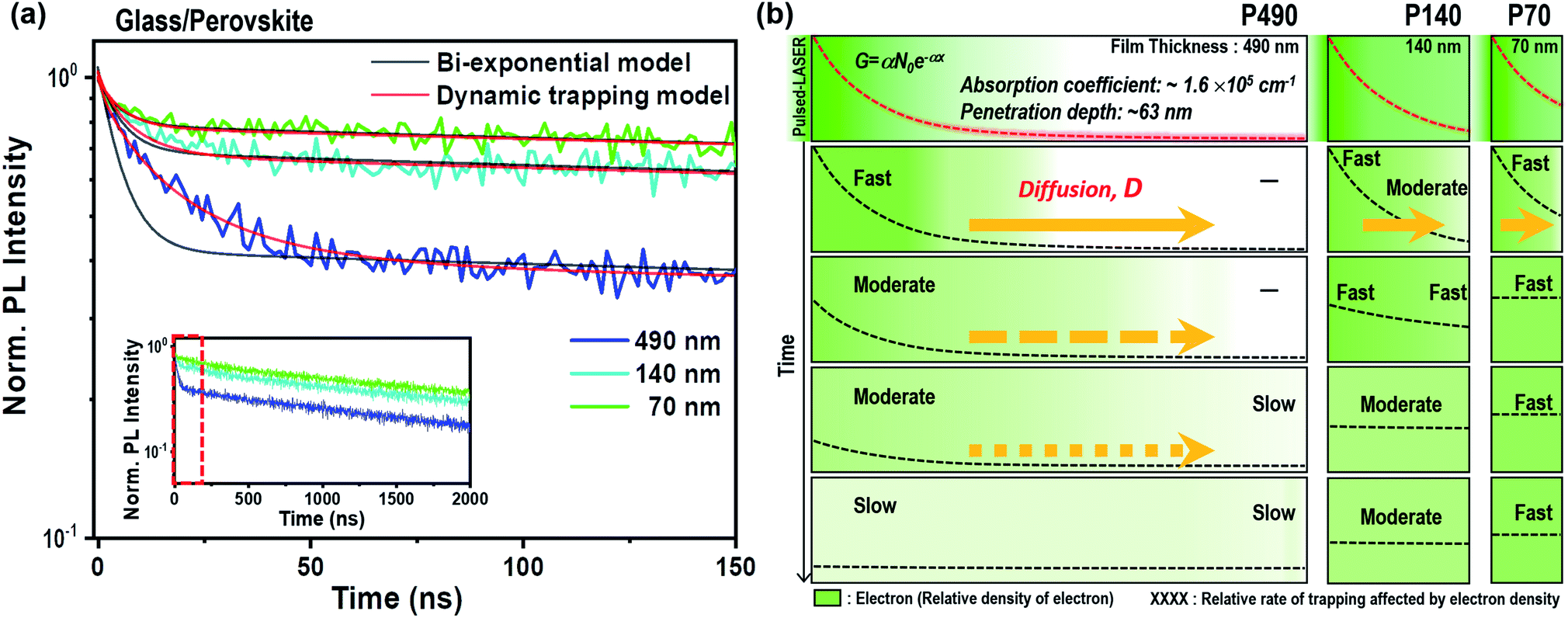 | ||
| Fig. 1 (a) The TRPL results of the neat perovskite thin films with different thicknesses (490, 140 and 70 nm) at a magnified time scale from 0 to 150 ns. The inset shows decay curves of each film up to 2000 ns. Experimental TRPL curves of each film were plotted together with the fitted curves using the bi-exponential function (black lines) and the dynamic trapping model function (red lines). (b) Schematic illustration of the electron distribution change within P490, P140 and P70 neat perovskite thin films over time. The dashed red lines represent initial electron generation in each film immediately after photo-excitation using a short-pulsed laser at a wavelength of 464 nm. The dashed black lines indicate the electron density distribution across the films as a function of distance from the light illumination side, and the brightness of the green color is an illustrative guide for the electron density. The black words (fast, moderate, slow and -) describe the relative rates of the trapping kinetics influenced by the electron densities, which changed the electron diffusion across the films (yellow arrows). | ||
Hence, we considered that the kinetics of the fast component, i.e., the SRH recombination, differed depending on the perovskite thickness in the TRPL results. As the thickness of the perovskite increased, the fast component appeared (1) larger in terms of intensity as well as (2) longer and stretched in terms of time. The difference in the intensities for the fast component originated from the difference in the electron density per volume. The difference in thickness not only resulted in a difference in the distance for an electron traveling to ETL, but also resulted in a difference in the electron density per volume in the perovskite layer. The total amounts of free electrons in P140 and P70 after instantaneous charge generation were 89.4% and 67.4%, respectively, compared to that of P490 (according to the calculation for the total quantity of electrons in the ESI†). However, the values for the electron density per volume of P140 and P70 were 3.1 and 4.7 times larger than that of P490, respectively. Therefore, the trapping process was more dominant than radiative recombination in P490 because the generated electron density per volume was smaller than that of P70; however, the trap density was identical. Second, the fast component of the TRPL decay curve appeared to be longer and stretched as the perovskite thickness increased because the trapping process is delayed by electron diffusion in a thick sample.
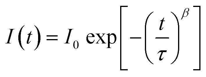
In Fig. 1b, we illustrate the change in the electron distribution of P490, P140 and P70 over time in neat perovskites after charge generation by a pulsed laser at a wavelength of 464 nm. We expected that P490, in comparison to thinner films, will need a relatively longer time to diffuse electrons due to a longer distance and a smaller electron density gradient at the side opposite to the illuminated surface. Indeed, in P490, near the illuminated surface, the trapping process immediately occurred after photo-excitation, whereas on the side opposite to the illuminated surface, the trapping process occurred after the electrons were filled by diffusion. This means that the rate of the trapping process can be delayed by the diffusion phenomenon, causing decrease in the rate constant (k), which can be interpreted by the stretched exponential function:3,29–31
 | (2) |
Therefore, here, we worked on the rapid diffusion of the initial high charge carrier density by correlating the trapping and diffusion processes for the neat perovskite film.32–35 We postulated that charge carriers dominantly travel via the out-of-plane direction (from the side of the illumination to the opposite side of the film). From the correlation between the electron trapping and diffusion processes on internal electron density, we suggested a modified fitting function, which is a combination of the stretched exponential function for a dynamic trapping model and the mono-exponential function for radiative recombination (eqn (3)):
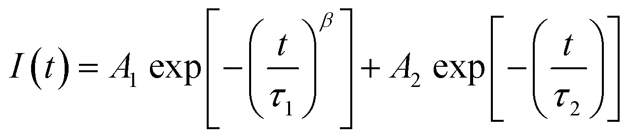 | (3) |
We performed both a modified fitting model (termed as a dynamic trapping model) and simple bi-exponential function; we have plotted the results together in Fig. 1a and Table S1.† The black lines indicate curves fitted with the simple bi-exponential function, and the red lines represent curves fitted with the dynamic trapping model. Apparently, in the fast time domain, the dynamic trapping model matched the experimental PL decay curves better than the simple bi-exponential function. The thicker the perovskite layer, the more stretched the exponential decay kinetics. Indeed, the β values obtained by fitting the results with the dynamic trapping model were 0.78, 0.87 and 0.95 for P490, 140 and P70, respectively. Notably, the fast component of P70 having a large β value close to 1 contained almost a consistent rate constant, which indicated the trapping process. A large average lifetime, 〈τ〉, calculated from the fast component, also signified the delayed trapping process by diffusion in the thicker film.
To demonstrate the interpretation of the above-mentioned phenomena, including the dynamic trapping model, we introduced a Synopsys Sentaurus Technology Computer-Aided Design (TCAD) platform after fine calibration, which is a computer simulation to develop and optimize semiconductor processing technologies and devices. The details of the simulation method and parameters are described and summarized in the ESI, Tables S2 and S3.† In Fig. 2a, we plot the spatiotemporal evolution of the electrons for P490, P140 and P70 after the generation of free electrons on the conduction band. As we discussed above, the thicker the perovskite film, the longer it takes for diffusion and flattening of the electron distribution throughout the film. Surprisingly, in Fig. 2b, we observe that the spatiotemporal evolution of the trapping rate for P490, P140 and P70 shows a very similar trend to that of the electron distribution in Fig. 2a. This means that the trapping rate is directly related to electron density. As the time for electron diffusion increased, it overlapped with the time domain for the trapping process and affected the kinetics of the trapping process, as depicted in Fig. 1b. We therefore believe that the dynamic trapping model is well explained by the simulation results. In other words, from the simulation results of electron decay by trapping processes with P490, P140 and P70 in Fig. 2c, we find that the decay rate constants for the trapping processes are nearly equal in the very fast time domain, i.e., below few nanoseconds. However, the slope of the decay curve for the P490 sample gradually became gentle, which indicated that the thicker sample followed a more stretched exponential behaviour in the trapping process, as can be seen from its degree of deviation from the straight line (only guide to eyes). In Fig. 2d, we show the experimental TRPL and corresponding simulation results. The simulated curves consistently express a change in the PL decay kinetics for the trapping process according to the thickness difference.
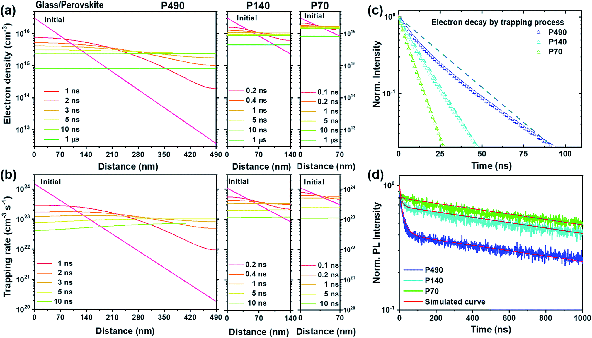 | ||
| Fig. 2 Spatiotemporal evolution of the electron densities (cm−3) by a simulation study and TRPL decay curves for P490, P140 and P70 perovskite thin films. (a) Spatiotemporal distribution of (b) electron densities and the trapping rate within P490, P140 and P70 neat perovskite thin films as a function of time after light illumination. (c) Simulation results of the electron decay by the trapping process within P490, P140 and P70. Dashed lines are a guide to eyes and are straight lines connecting the starting point and 0.02 values in each normalized decay curves. (d) Experimental TRPL results with corresponding simulation results (red solid lines). | ||
Charge carrier injection and mobility for diffusion process
In a real device architecture, charge quenching layers influence the charge transport processes at the interfaces. We assessed if the charge extraction by (or injection to) the quenching layer at the side opposite to light illumination influenced the charge transport processes we discussed above i.e., charge trapping and diffusion throughout the perovskite thin film. Thus, we here introduced the electron transport layer (SnO2) at the side opposite to the light illumination. We note that although only the electron extraction process was added in the SQ-TRPL measurement in comparison to TRPL, the rate constant measured by SQ-TRPL was the result of a combination of the electron injection coefficient (ki), electron mobility (μe) of perovskite, quality of physical contact, thickness of the sample and the initial charge distribution.13,36,37 In this study, we considered the constant value of charge carrier mobility with respect to film thickness28 and excitation density (1014–1016 cm−3) because in ideal semiconductors, mobility is independent of charge carrier density until carrier–carrier scattering effects become an important factor.38In Fig. 3a, we illustrate the change in electron distribution over time for P490, P140 and P70 perovskite thin films with ETL. For interfacial charge extraction, electrons should diffuse to the interface between the perovskite and ETL. As depicted in the schematic illustration, we can expect that μe of the perovskite would be important for a longer diffusion in a thicker film, whereas ki at the interface would be important for a shorter diffusion in thinner films. Hence, we can assume that a bigger ki value would result in a steep electron density gradient near the interface. In other words, the bigger ki value induces faster diffusion in the bulk of the perovskite.
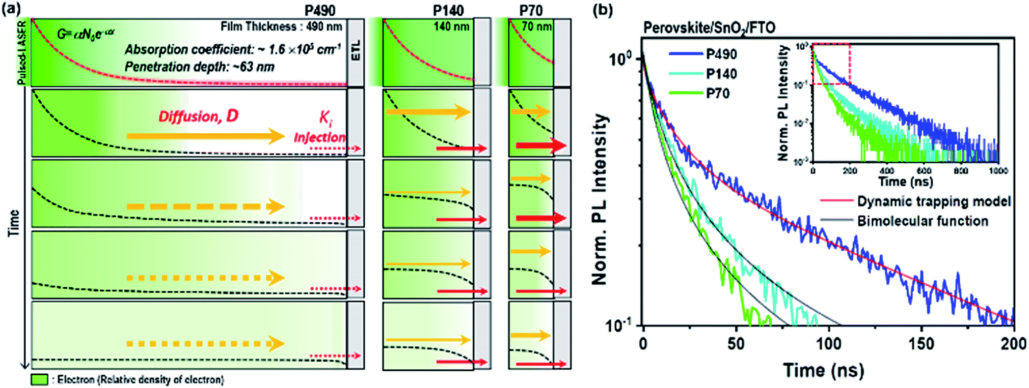 | ||
| Fig. 3 Schematic illustration of electron distribution change across the perovskite thin films with ETL and experimental TRPL data. (a) Illustration of electron distribution change across the perovskite thin films with a surface quencher ETL for P490, P140 and P70 over time. The dashed red lines represent the initial electron generation in each film immediately after the photo-excitation using short pulsed laser at a wavelength of 464 nm. The dashed black lines indicate the electron density distribution across the films as a function of distance from light illumination side, and the brightness of green color is an illustrative guide of the electron density. Red arrows describe relative rates of injection at the interface between perovskite thin films and ETL. (b) SQ-TRPL results of perovskite thin films with SnO2 in the magnified time scale from 0 to 200 ns. The inset shows decay curves of each film up to 1000 ns. Experimental TRPL curves of each film are plotted together with fitted curves using the bimolecular function (black lines) for P140 and P70, and the dynamic trapping model function (red lines) for P490. | ||
The SQ-TRPL results for P490, P140 and P70 perovskite thin films with SnO2 ETL are plotted in Fig. 3b. Taking a closer look at the red square part of the entire decay curves in the inset, a notable change in the PL decay curves is observed when the thickness of the perovskite layer is reduced from 490 to 140 and 70 nm. The PL decay curve of P490 shows bi-exponential-like decay kinetics, but the PL decay curves of P140 and P70 show very fast bimolecular decay kinetics, in which the distinction between the fast and the slow components disappears. The charge transfer kinetics during electron extraction at the interface was associated with the electronic coupling element, which contributed to free electrons at the conduction band of perovskites and density of states in an n-type semiconductor. When the electron density (n) in the perovskite near the interface with ETL was smaller compared to the density of states at ETL, the extraction process appeared as a monomolecular decay kinetic proportional to n, whereas when n and the density of states at ETL had comparable values, the extraction process followed the bimolecular decay kinetic proportional to n2.9 Hence, SQ-TRPL with P490 was fitted to the dynamic trapping model, and P140 and P70 were fitted to the second-order rate reaction equation representing bimolecular decay kinetics (Fig. 3b and Table S4†). For the P140 and P70 samples, the linear part at the early-time region in the reciprocal plot (Fig. S8†) indicates bimolecular extraction kinetics due to the large electron density (n) near the interface with ETL. The extracted τ1 and β values, indicating the trapping process, were 13.5 ns and 0.79 for the P490/SnO2 sample, respectively. These values were reliably similar to the ones obtained from the neat perovskite film, which meant that the origin of the fast component in TRPL was identical to SQ-TRPL. The τ2 value for the P490/SnO2 sample, a newly generated decay component, was 133.2 ns, which we attributed to the electron extraction process. For the P140 and P70 samples, we found that the extraction process was a much faster decay kinetic than the trapping process. The bimolecular rate coefficient, k2, values for the P140 and P70 samples were 8.47 × 10⁷ and 1.16 × 108 cm3 s−1, respectively. The intrinsic ki value at the interface between the perovskite and ETL was closer to the k2 value obtained for P70 because the value of ki becomes a more critical determinant at short distances.
We showed the spatiotemporal evolutions of electrons by a simulation study for P490, P140 and P70 with SnO2 ETL after free electron generation on the conduction band, as shown in Fig. 4a. For the shorter diffusion distance, the electron density gradient became steeper near the interface with ETL. In Fig. 4b, with the experimental SQ-TRPL data, the simulated curves (red solid lines) express a change in the kinetics of the extraction process, including bimolecular decay kinetics with thickness differences. To demonstrate the importance of the τ2 value for the P490 sample with ETL, we varied the fitting parameters (injection rate constant and electron mobility) in further simulation studies (Fig. 4c, d and S9†). When the ki value increased by an order of magnitude for the P490 sample (dotted blue line in Fig. 4c), the PL decayed faster and indeed became similar to that of the untouched P70 sample (green solid line). On the other hand, when ki was an order of magnitude smaller (dashed blue line), the fast component in the early-time region (i.e., the trapping process) did not change, but the slow component (i.e., the extraction process) slowed down. For the P70 sample with ETL, when the ki value increased by an order of magnitude (dotted green line), the PL decayed dramatically fast, whereas the PL decay curve showed a similar shape to that of the original P490 when the ki value was an order of magnitude smaller (dashed green line). In comparison to the distinctive changes in the PL decays with different injection rate constants, when μe was increased by an order of magnitude (blue and green dotted lines in Fig. 4d) for both the P490 and P70 samples, the PL decays were analogous to the initial decays in both samples. Notably, with an order of magnitude smaller μe for the P490 sample, an unchanged slow component of the PL decay represented a similar electron extraction rate to the PL decay with its initial mobility value. On the other hand, the fast component slowed down because the trapping process was relatively dominant during the initial diffusion process, as we discussed with the dynamic trapping model above. These phenomena reversely resulted in an order of magnitude smaller μe for the P490 sample, indicating a slightly decelerated extraction process.
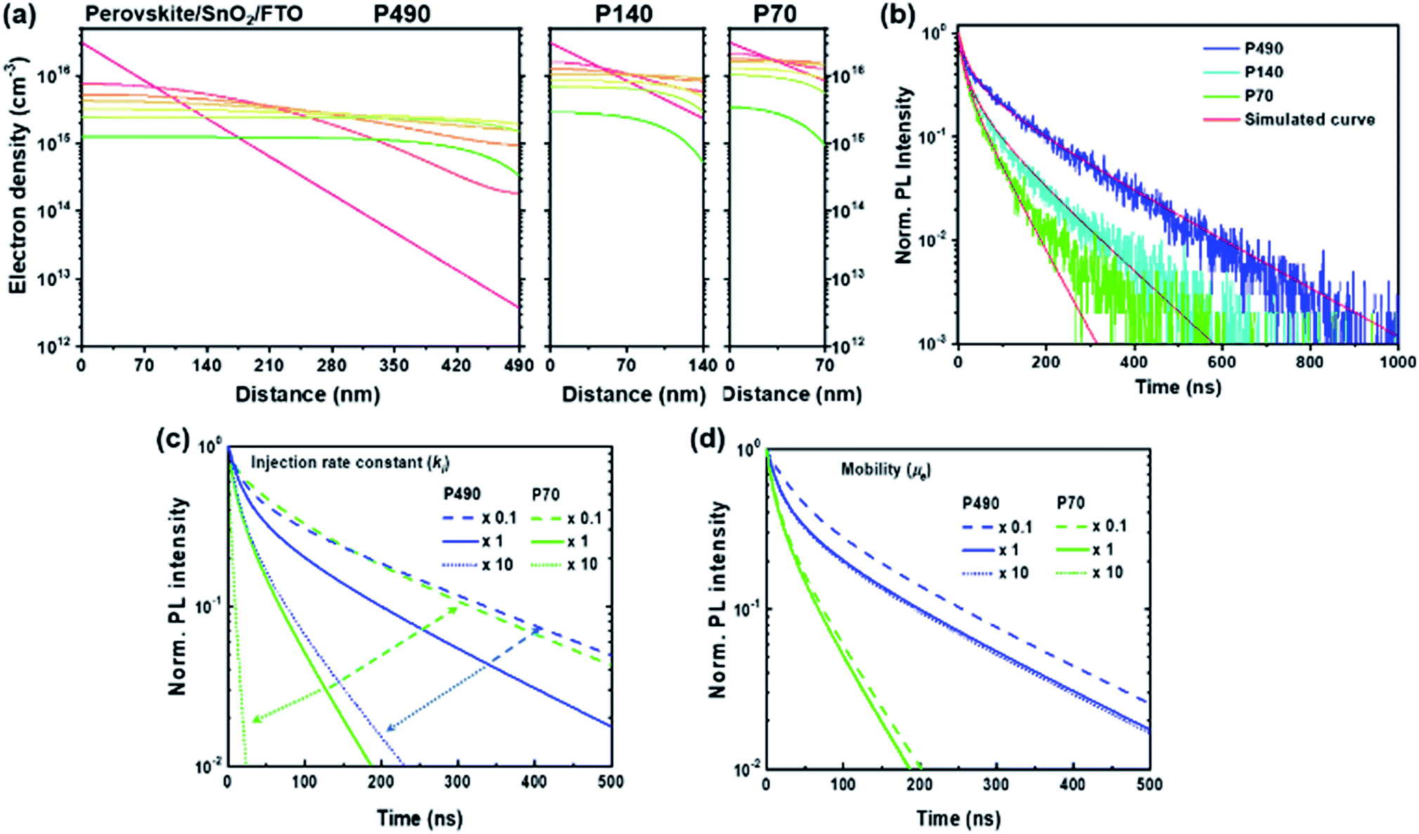 | ||
| Fig. 4 Spatiotemporal evolution of the electron density (cm−3) by the simulation study for P490, P140 and P70 with the SnO2 ETL. (a) Electron density distribution across the perovskite thin films with the surface quencher SnO2 ETL. (b) Experimental SQ-TRPL results and corresponding simulation results (red solid lines). Normalized PL intensity decay curves with different (c) injection rate constant (ki) (dotted and dashed arrows are only a guide to eyes) and (d) electron mobility (μe) at an order of magnitude lower (dashed lines) and higher (dotted lines) than the initial values (solid lines) for perovskite thin films P490 (blue lines) and P70 (green lines) with the surface quencher SnO2 ETL. | ||
From the simulation results showing the sensitive change in the electron extraction kinetics with the ki values rather than the μe value, we found that the μe value, i.e., 3 cm2 V−1 s−1 in the simulation study was sufficiently high for the electron extraction process. Therefore, ki was the more critical determinant for the electron extraction process compared to μe. Furthermore, our study demonstrated that the slow component in SQ-TRPL involved information about ki using the one-dimensional diffusion equation.
We note that there were differences in charge transport related to properties such as perovskite composition,14 grain sizes39,40 and crystal orientation, which can also be explained by trapping/detrapping processes,41 grain-boundary scattering,42,43 and charging at grain boundaries. To extend our investigation in this study for further understanding, we studied the role of grain sizes in PL lifetimes with respect to the direction of charge carrier diffusion.
Conclusions
In summary, we developed a theoretical model describing the interrelations between the trapping and diffusion processes of electrons for perovskites. The dynamic trapping model reproduced the stretched exponential PL decay in the trapping process. The results suggested that electron mobility can influence the kinetics of the trapping process in transient state spectroscopy. Consequently, in addition to the slow component in SQ-TRPL, we demonstrated that the rate of the electron extraction process was limited not by the electron mobility (μe) of perovskite but by the injection rate constant (ki) for the interface between the perovskite and ETL. Our work can support the interpretation of PL decay kinetics for a lead halide perovskite light absorber material. Our work also reveals a new parameter for the future optimisation of optoelectronic devices using quantum dots, carbon materials, semiconducting organic molecules and metal oxides. We also believe that extended work on this study can support further understanding of recombination processes in solar cell systems under white light illumination.Conflicts of interest
The authors declare no competing financial interest.Acknowledgements
This work was supported by the National Research Foundation of Korea (NRF) grant (2018R1A2A1A05079144), which was funded by the Korea government (MSIP), and by the NRF grant (2016M1A2A2940912), which was funded by the Korea Government (MSIP). The Synopsys Sentaurus TCAD tool was supported by the IC Design Education Center.References
- S. D. Stranks, G. E. Eperon, G. Grancini, C. Menelaou, M. J. P. Alcocer, T. Leijtens, L. M. Herz, A. Petrozza and H. J. Snaith, Science, 2013, 342, 341–344 CrossRef CAS PubMed.
- G. Xing, N. Mathews, S. Sun, S. S. Lim, Y. M. Lam, M. Grätzel, S. Mhaisalkar and T. C. Sum, Science, 2013, 342, 344–347 CrossRef CAS PubMed.
- D. W. DeQuilettes, S. M. Vorpahl, S. D. Stranks, H. Nagaoka, G. E. Eperon, M. E. Ziffer, H. J. Snaith and D. S. Ginger, Science, 2015, 348, 683–686 CrossRef CAS PubMed.
- M. Maiberg and R. Scheer, J. Appl. Phys., 2014, 116, 123710 CrossRef.
- M. Maiberg and R. Scheer, J. Appl. Phys., 2014, 116, 123711 CrossRef.
- E. M. Y. Lee and W. A. Tisdale, J. Phys. Chem. C, 2015, 119, 9005–9015 CrossRef CAS.
- S. Makuta, M. Liu, M. Endo, H. Nishimura, A. Wakamiya and Y. Tachibana, Chem. Commun., 2016, 52, 673–676 RSC.
- S. Song, G. Kang, L. Pyeon, C. Lim, G. Y. Lee, T. Park and J. Choi, ACS Energy Lett., 2017, 2, 2667–2673 CrossRef CAS.
- S. D. Stranks, V. M. Burlakov, T. Leijtens, J. M. Ball, A. Goriely and H. J. Snaith, Phys. Rev. Appl., 2014, 2, 1–8 Search PubMed.
- G. W. Kim, J. Lee, G. Kang, T. Kim and T. Park, Adv. Energy Mater., 2018, 8, 1–5 Search PubMed.
- J. P. Correa-Baena, S. H. Turren-Cruz, W. Tress, A. Hagfeldt, C. Aranda, L. Shooshtari, J. Bisquert and A. Guerrero, ACS Energy Lett., 2017, 2, 681–688 CrossRef CAS.
- E. M. Hutter, J. J. Hofman, M. L. Petrus, M. Moes, R. D. Abellón, P. Docampo and T. J. Savenije, Adv. Energy Mater., 2017, 7, 1–8 Search PubMed.
- F. Staub, H. Hempel, J. C. Hebig, J. Mock, U. W. Paetzold, U. Rau, T. Unold and T. Kirchartz, Phys. Rev. Appl., 2016, 6, 1–13 Search PubMed.
- J. Lim, M. T. Hörantner, N. Sakai, J. M. Ball, S. Mahesh, N. K. Noel, Y. H. Lin, J. B. Patel, D. P. McMeekin, M. B. Johnston, B. Wenger and H. J. Snaith, Energy Environ. Sci., 2019, 12, 169–176 RSC.
- J. D. A. Lin, O. V. Mikhnenko, J. Chen, Z. Masri, A. Ruseckas, A. Mikhailovsky, R. P. Raab, J. Liu, P. W. M. Blom, M. A. Loi, C. J. García-Cervera, I. D. W. Samuel and T. Q. Nguyen, Mater. Horiz., 2014, 1, 280–285 RSC.
- Z. Bin, J. Li, L. Wang and L. Duan, Energy Environ. Sci., 2016, 9, 3424–3428 RSC.
- J. Song, L. Liu, X. F. Wang, G. Chen, W. Tian and T. Miyasaka, J. Mater. Chem. A, 2017, 5, 13439–13447 RSC.
- Y. Sun, J. Peng, Y. Chen, Y. Yao and Z. Liang, Sci. Rep., 2017, 7, 1–7 CrossRef PubMed.
- D.-X. Yuan, A. Gorka, M.-F. Xu, Z.-K. Wang and L.-S. Liao, Phys. Chem. Chem. Phys., 2015, 17, 19745–19750 RSC.
- K. Lee, K. H. Cho, J. Ryu, J. Yun, H. Yu, J. Lee, W. Na and J. Jang, Electrochim. Acta, 2017, 224, 600–607 CrossRef CAS.
- Y. Yamada, T. Nakamura, M. Endo, A. Wakamiya and Y. Kanemitsu, J. Am. Chem. Soc., 2014, 136, 11610–11613 CrossRef CAS PubMed.
- D. Shi, V. Adinolfi, R. Comin, M. Yuan, E. Alarousu, A. Buin, Y. Chen, S. Hoogland, A. Rothenberger, K. Katsiev, Y. Losovyj, X. Zhang, P. A. Dowben, O. F. Mohammed, E. H. Sargent and O. M. Bakr, Science, 2015, 347, 519–522 CrossRef CAS PubMed.
- E. M. Hutter, G. E. Eperon, S. D. Stranks and T. J. Savenije, J. Phys. Chem. Lett., 2015, 6, 3082–3090 CrossRef CAS PubMed.
- W. Tian, C. Zhao, J. Leng, R. Cui and S. Jin, J. Am. Chem. Soc., 2015, 137, 12458–12461 CrossRef CAS PubMed.
- S. M. Olaizola, W. H. Fan, S. A. Hashemizadeh, J. P. R. Wells, D. J. Mowbray, M. S. Skolnick, A. M. Fox and P. J. Parbrook, Appl. Phys. Lett., 2006, 89, 072107 CrossRef.
- W. Shockley and W. T. Read, Phys. Rev., 1952, 87, 835–842 CrossRef CAS.
- M. Saliba, T. Matsui, J. Y. Seo, K. Domanski, J. P. Correa-Baena, M. K. Nazeeruddin, S. M. Zakeeruddin, W. Tress, A. Abate, A. Hagfeldt and M. Grätzel, Energy Environ. Sci., 2016, 9, 1989–1997 RSC.
- T. W. Crothers, R. L. Milot, J. B. Patel, E. S. Parrott, J. Schlipf, P. Müller-Buschbaum, M. B. Johnston and L. M. Herz, Nano Lett., 2017, 17, 5782–5789 CrossRef CAS PubMed.
- A. V. Milovanov, K. Rypdal and J. J. Rasmussen, Phys. Rev. B: Condens. Matter Mater. Phys., 2007, 76, 1–8 CrossRef.
- X. Chen, B. Henderson and K. P. O'Donnell, Appl. Phys. Lett., 1992, 60, 2672–2674 CrossRef CAS.
- M. Pophristic, F. H. Long, C. Tran, I. T. Ferguson and R. F. Karlicek, Appl. Phys. Lett., 1998, 73, 3550–3552 CrossRef CAS.
- W. Tian, R. Cui, J. Leng, J. Liu, Y. Li, C. Zhao, J. Zhang, W. Deng, T. Lian and S. Jin, Angew. Chem., Int. Ed., 2016, 55, 13067–13071 CrossRef CAS PubMed.
- C. Zhao, W. Tian, J. Leng, R. Cui, W. Liu and S. Jin, Sci. Bull., 2016, 61, 665–669 CrossRef CAS.
- N. K. Noel, A. Abate, S. D. Stranks, E. S. Parrott, V. M. Burlakov, A. Goriely and H. J. Snaith, ACS Nano, 2014, 8, 9815–9821 CrossRef CAS PubMed.
- A. Abate, M. Saliba, D. J. Hollman, S. D. Stranks, K. Wojciechowski, R. Avolio, G. Grancini, A. Petrozza and H. J. Snaith, Nano Lett., 2014, 14, 3247–3254 CrossRef CAS PubMed.
- J. A. Christians, D. T. Leighton and P. V. Kamat, Energy Environ. Sci., 2014, 7, 1148–1158 RSC.
- C. Liu, G. Huseynova, Y. Xu, D. X. Long, W. T. Park, X. Liu, T. Minari and Y. Y. Noh, Sci. Rep., 2016, 6, 1–14 CrossRef CAS PubMed.
- O. Flender, J. R. Klein, T. Lenzer and K. Oum, Phys. Chem. Chem. Phys., 2015, 17, 19238–19246 RSC.
- N. K. Noel, S. N. Habisreutinger, B. Wenger, M. T. Klug, M. T. Hörantner, M. B. Johnston, R. J. Nicholas, D. T. Moore and H. J. Snaith, Energy Environ. Sci., 2017, 10, 145–152 RSC.
- W. Zhang, S. Pathak, N. Sakai, T. Stergiopoulos, P. K. Nayak, N. K. Noel, A. A. Haghighirad, V. M. Burlakov, D. W. Dequilettes, A. Sadhanala, W. Li, L. Wang, D. S. Ginger, R. H. Friend and H. J. Snaith, Nat. Commun., 2015, 6, 10030 CrossRef CAS PubMed.
- T. Leijtens, S. D. Stranks, G. E. Eperon, R. Lindblad, E. M. J. Johansson, I. J. McPherson, H. Rensmo, J. M. Ball, M. M. Lee and H. J. Snaith, ACS Nano, 2014, 8, 7147–7155 CrossRef CAS PubMed.
- J. Steinhauser, S. Faÿ, N. Oliveira, E. Vallat-Sauvain and C. Ballif, Appl. Phys. Lett., 2007, 90, 1–4 CrossRef.
- A. A. Paraecattil, J. De Jonghe-Risse, V. Pranculis, J. Teuscher and J. E. Moser, J. Phys. Chem. C, 2016, 120, 19595–19602 CrossRef CAS.
Footnotes |
| † Electronic supplementary information (ESI) available: Details of experiments, supplementary note, Tables S1–S4, Fig. S1–S9. See DOI: 10.1039/c9ta06254h |
| ‡ These authors contributed equally to this work. |
| This journal is © The Royal Society of Chemistry 2019 |