
The effect of structural dimensionality on carrier mobility in lead-halide perovskites†
Noor Titan Putri
Hartono
 a,
Shijing
Sun
a,
María C.
Gélvez-Rueda
b,
Polly J.
Pierone
c,
Matthew P.
Erodici
c,
Jason
Yoo
a,
Fengxia
Wei
d,
Moungi
Bawendi
a,
Ferdinand C.
Grozema
b,
Meng-ju
Sher
c,
Tonio
Buonassisi
*a and
Juan-Pablo
Correa-Baena
*a
a,
Shijing
Sun
a,
María C.
Gélvez-Rueda
b,
Polly J.
Pierone
c,
Matthew P.
Erodici
c,
Jason
Yoo
a,
Fengxia
Wei
d,
Moungi
Bawendi
a,
Ferdinand C.
Grozema
b,
Meng-ju
Sher
c,
Tonio
Buonassisi
*a and
Juan-Pablo
Correa-Baena
*a
aMassachusetts Institute of Technology, 77 Massachusetts Avenue, Cambridge, MA 02139, USA. E-mail: buonassisi@mit.edu; jpcorrea@mit.edu
bDelft University of Technology, van der Maasweg 9, 2629 HZ Delft, The Netherlands
cWesleyan University, 265 Church Street, Middletown, CT 06459, USA
dInstitute of Materials Research and Engineering, A*STAR, 2 Fusionopolis Way, Innovis, Singapore 138634
First published on 9th July 2019
Abstract
Methylammonium lead iodide (MAPI) is a prototypical photoabsorber in perovskite solar cells (PSCs), reaching efficiencies above 20%. However, its hygroscopic nature has prompted the quest for water-resistant alternatives. Recent studies have suggested that mixing MAPI with lower dimensional, bulky-A-site-cation perovskites helps mitigate this environmental instability. On the other hand, low dimensional perovskites suffer from poor device performance, which has been suggested to be due to limited out-of-plane charge carrier mobility resulting from structural dimensionality and large binding energy of the charge carriers. To understand the effects of dimensionality on performance, we systematically mixed MA-based 3D perovskites with larger A-site cations to produce dimethylammonium, iso-propylammonium, and t-butylammonium lead iodide perovskites. During the shift from MAPI to lower dimensional (LD) PSCs, the efficiency is significantly reduced by 2 orders of magnitude, with short-circuit current densities decreasing from above 20 mA cm−2 to less than 1 mA cm−2. In order to explain this decrease in performance, we studied the charge carrier mobilities of these materials using optical-pump/terahertz-probe, time-resolved microwave photoconductivity, and photoluminescence measurements. The results show that as we add more of the low dimensional perovskites, the mobility decreases, up to a factor of 20 when it reaches pure LD perovskites. In addition, the photoluminescence decay fitting is slightly slower for the mixed perovskites, suggesting some improvement in the recombination dynamics. These findings indicate that changes in structural dimensionality brought about by mixing A-site cations play an important role in determining the measured charge carrier mobility, and in the performance of perovskite solar cells.
Introduction
Organic lead halide perovskite solar cells (PSCs) have reached high efficiencies in just 9 years, with a current record efficiency of 24.2%.1,2 However, PSCs still face challenges towards commercialization, such as environmental stability. The most widely studied perovskite, methylammonium lead iodide (MAPI), decomposes readily into lower dimensional perovskite structures at standard temperature and pressure, and in some cases where oxygen, ultraviolet radiation, and moisture are present, the methylammonium iodide can degrade further.3 Mixing MAPI perovskites with bulkier A-site cations, to produce perovskites such as (PEA)2(MA)2[Pb3I10], where PEA is phenethylammonium and MA is methylammonium, forming layered structures (or lower dimensional, LD) instead of 3-dimensional (3D) structures as in the case of MAPI, can improve the long-term stability of the PSCs.4–6 Researchers have also tried mixing 3D perovskites with small amounts of bulky A-site cations, such as n-butylammonium,7,8 ethylenediamine,9 and 2-hydroxyethylamine.10 However, adding high amounts of bulky A-site cations in 3D perovskite mixtures results in lower device performance in comparison to their 3D analogues.4,11,12 A recent study investigating the effects of LD perovskites on solar cell performance suggests that LD perovskites with a layered structure have a strong preferred in-plane orientation due to air–liquid interface nucleation.13 This suggests that most charge transport occurs in the in-plane instead of the out-of-plane direction, which is unfavorable for charge extraction in solar cells. In addition, the interplay between the perovskite dimensionality and its solar cell performance is not well understood.Important parameters which determine solar cell performance are the charge carrier diffusion coefficient (D) and lifetime (τ). The carrier lifetime of various halide perovskites, both lead-based and lead-free, is relatively long, and exceeds hundreds of nanoseconds.14–17 On the other hand, the diffusion coefficient, which linearly depends on the charge-carrier mobility, is still not well understood for LD perovskites. Hence, a deeper look at the charge-carrier mobility of LD perovskites will give a more complete picture of the diffusion length, and its relationship with solar cell performance. This understanding will serve as an initial proxy for the interplay between device performance and structural dimensionality.
In this study, we intentionally broke down the high-performance, 3D-based perovskite devices by systematically mixing 3D perovskites (methylammonium lead iodide, MAPI) with LD ones, which allowed us to investigate the fundamental mechanism behind performance reduction incrementally. Three bulky A-site cations were used to impose structural changes within the lattice: dimethylammonium, iso-propylammonium, and t-butylammonium. Based on pre-defined precursor volume ratios of MAPI and the LD APbI3, the MAPI 3D structure with octahedral corner-sharing was forced to split into single-chained edge-sharing and corner-sharing (1D) perovskites. The solar cell performance was dramatically affected. In addition to efficiency (PCE), short-circuit current density (JSC), and open-circuit voltage (VOC), we also calculated WOC (bandgap-voltage offset under open-circuit conditions) and ΔJnormSC (short-circuit current density deficit normalized) using the following equations (eqn (1) and (2)):
 | (1) |
 | (2) |
Results and discussion
Crystallographic information
Methylammonium lead iodide (CH3NH3PbI3, MAPI, or M), with a known 3D cubic structure,18 was mixed in different volume-based ratios with layered or single-chain perovskites: dimethylammonium lead iodide (((CH3)2NH)2PbI4, DMAPI, or D), iso-propylammonium lead iodide (((CH3)2CHNH3)3PbI5, iPAPI, or I), or t-butylammonium lead iodide (((CH3)3CNH3)2PbI4, tBAPI, or T). The D, I, and T bulky A-site cations were chosen specifically due to their gradual change in ionic radii, which affects the tolerance factor and the dimensionality of the perovskite structure. Goldschmidt's tolerance factor is an empirical unit used to describe the 3D perovskite structure based on the ionic radii of the A-site cation, the B-site cation, and/or the X-site anion. The adequate range for 3D perovskites is 0.8 to 1.0 as shown in eqn (3):19–21 | (3) |
The tolerance factors of D, I, and T are obtained from eqn (3), using the effective radii for the A-site cations (dimethylammonium = 2.72 Å, iso-propylammonium = 3.17 Å, and t-butylammonium = 4.94 Å), the B-site cation (Pb2+ = 1.19 Å), and X-anion (I− = 2.2 Å).19–21 A tolerance factor of 1.03 was found for D, 1.12 for I, and 1.49 for T, as shown in Fig. 1A, in contrast to M, which has a tolerance factor of 0.91. In comparison, the common LD perovskite used, n-butylammonium lead iodide, has a tolerance factor of 1.001.22 In this study, to mix the perovskites, the precursor solutions of two different types of perovskites (for instance, MAPI and tBAPI) were mixed in 3 different ratios: 75%![[thin space (1/6-em)]](https://www.rsc.org/images/entities/char_2009.gif) :25%, 50%:50%, and 25%:75%. Thin films were prepared following standard approaches.23 The perovskite film was made with excess PbI2 (AI:PbI2 = 1:1.09 for APbI3) as this strategy has been shown to yield improved solar cell performance.24,25
:25%, 50%:50%, and 25%:75%. Thin films were prepared following standard approaches.23 The perovskite film was made with excess PbI2 (AI:PbI2 = 1:1.09 for APbI3) as this strategy has been shown to yield improved solar cell performance.24,25
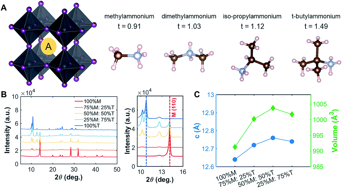 | ||
| Fig. 1 Crystallographic features of the perovskites studied. (A) Various A-site cations (M, D, I, and T) with their tolerance factors. The single crystal structures for D, I, and T are shown in ESI Fig. S1.† (B) The peak shift shown for the M–T series in the thin-film form. As more T was added into the film, the peak of the LD perovskite became more evident. (C) For the thin films, the lattice parameters (c and volume) increased as more T was added into M, indicating that the large A-site cation did get incorporated into the lattice. | ||
To understand the effects of mixing on the structural properties, we prepared thin films with series of different ratios of MAPI to LD perovskites: MAPI–DMAPI (M–D), MAPI–iPAPI (M–I), and MAPI–tBAPI (M–T) series. We performed X-ray diffraction (XRD) on these thin films. The results were then refined using Pawley refinement, and the lattice parameters of the phases were obtained. Fig. 1B shows how the addition of T affects the XRD patterns. One signature peak of 100% M is located at 14.1°. As more T was added to M perovskites, the intensity of the 14.1° peak decreased, and another peak emerged at 10.8°, suggesting that a secondary phase of LD material formed within the polycrystalline thin film. To quantify how the lattice parameters of M increase with this mixing, we performed Pawley refinement of the M–T series. The lattice parameters, lattice constant and cell volume, are shown in Fig. 1C. As more T was added to the M perovskite, the lattice constants increased, suggesting that the larger A-site cation has an effect on the structural features of the M perovskite, in addition to the secondary phase formed. Similar trends of lattice parameter increase were observed for the M–D and M–I series, and the data are provided in ESI Fig. S3.†
Optical properties
The 3D/LD hybrid perovskite thin films deposited on glass (M–D, M–I, and M–T) are shown in Fig. 2A. A gradual change of the film colors, ranging from dark to light yellow, was observed. On the other hand, mixing LD and other LD hybrid perovskites (D–I, D–T, and I–T) yielded no visible changes.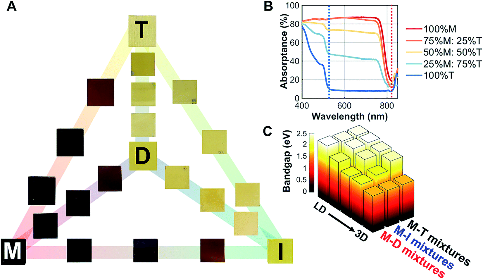 | ||
| Fig. 2 Optical properties of the 3D/low dimensional perovskites studied here. (A) Thin films of methylammonium lead iodide (M) mixed with dimethylammonium lead iodide (D), iso-propylammonium lead iodide (I), and t-butylammonium lead iodide (T) with set ratios: 100%:0%, 75%:25%, 50%:50%, 25%:75%, and 0%:100%. The 100% M, D, I, and T films are indicated with the corresponding letters on the films. (B) Absorption of the M–T series, where two absorption onsets are shown at 525 and 825 nm. (C) The direct bandgap estimated by Tauc plots for the M–D, M–I, and M–T series at the 525 nm onset; a secondary phase bandgap estimation resulting from the 825 nm onset is shown in ESI Fig. S7.† | ||
To understand the changes in optical absorption of these mixed perovskites, UV/Vis spectroscopy was performed from 840 nm to 400 nm (Fig. 2B) in thin films. As we mixed M with T, two onsets appeared, one at 825 nm (100% M absorption onset) and another at 525 nm (100% T absorption onset). Both 100% D and 100% I absorption profiles had similar onsets to 100% T, as shown in ESI Fig. S4.† Tauc plot fitting was then performed to estimate the band gap for these films (fits can be found in ESI Fig. S5†). A non-linear increase in direct bandgap estimation was observed as the perovskites were mixed from 3D to LD for both absorption onsets. Additionally, the steady-state photoluminescence data for M–T series in ESI Fig. S6† showed a slight emission shift in the first absorption onset (825 nm). The bandgaps were estimated as 1.57 eV for M, 2.39 eV for D, 2.35 eV for I, and 2.34 eV for T, as shown in Fig. 2C.
Device performance
To understand how mixing 3D with LD perovskites affects the device performance, we fabricated 120 devices for all M–D, M–I, and M–T series, and we measured the solar cell performance under an AM1.5G solar simulator under 1.0 sun operating conditions. The best solar cell J–V (current density–voltage) curve data from this measurement are provided in ESI Fig. S8,† and the complete device performance results are shown in ESI Tables S1 and S2.† We expect that as we shift from 3D PSCs to LD PSCs, the solar cell performance will be affected due to the reduction in structural dimensionality. Solar cells were prepared as shown in the schematic and SEM image in Fig. 3A. Fluorine-doped tin oxide (FTO) glass was used as the transparent conducting oxide, followed by the electron selective TiO2 compact and mesoporous layers and the hole transport spiro-OMeTAD layer, followed by a gold layer deposited from thermal evaporation as the top electrode. The top-down scanning electron microscopy (SEM) images for the M–T series can also be seen in ESI Fig. S9.†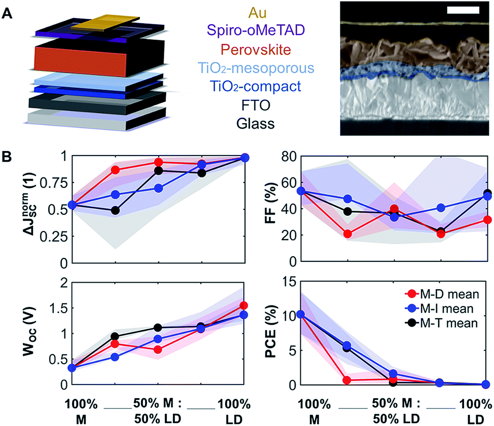 | ||
| Fig. 3 Solar cell performance parameters of the 3D/LD mixed perovskites. (A) A schematic and a SEM image (artificially colored) for the device stack of the 25% M:75% T device, 500 nm scale bar. (B) The plot and average of solar cell performance metrics for M–D, M–I, and M–T series, including ΔJnormSC (short-circuit current density deficit normalized), calculated by normalizing the difference between the theoretical maximum bandgap-specific JSC with the measured JSC, WOC (bandgap-voltage offset under open-circuit conditions), calculated by subtracting the Shockley–Queisser limit, bandgap-specific VOC from the measured VOC, FF (fill factor), and PCE (power conversion efficiency). The shaded area shows the results between the 25th and 75th percentiles. | ||
The solar cell performance parameters, including ΔJnormSC (short-circuit current density deficit normalized), FF (fill factor), WOC (bandgap-voltage offset under open-circuit conditions), and PCE (power conversion efficiency), are shown in Fig. 3B. WOC is the difference between the Shockley–Queisser limit VOC for a specific bandgap at AM1.5G and the actual device VOC. The WOC shown in Fig. 3B is based on the 525 nm absorption onset, and the WOC based on the 825 nm onset is shown in ESI Fig. S10.† The WOC values for both onsets increase with shifting from 3D to LD materials. All solar cells experienced a decrease in JSC as the bulky A-site cations (D, I, and T) were mixed with MAPI. For example, the JSC for 100% M was measured to be 16–20 mA cm−2, decreasing to 0.1–0.5 mA cm−2 for 100% T, a 1–2 order of magnitude reduction, which corresponds to a 1.8 times increase in ΔJnormSC. The WOC increased by 4.2 times as we shifted from 3D (M) to 1D (D, I, and T) perovskites. No major changes in FF were found as a function of mixing. Both increases in ΔJnormSC and WOC led to a large drop in solar cell efficiency across all the series.
Even at relatively low concentrations of LD perovskites, e.g. 75% M and 25% of the LD perovskites, the efficiency dropped dramatically. This can be related to the changes seen in XRD data (Fig. 1B), where as little as 25% of the LD perovskite yields phase segregation. A study has suggested that there is an optimum PCE for Ruddlesden–Popper perovskite solar cell devices, with a low n, which represents the number of 3D perovskite layers sandwiched between LD perovskites.26 There is a possibility that the optimum device performance can be reached at an LD perovskite concentration lower than 25%, which is not captured in Fig. 4B. The introduction of secondary phases of LD characteristics can also induce changes in how charge carriers move across the thin film. Mobility of charge carriers is directly proportional to the diffusion length of the perovskite material. We studied the charge carrier mobility using an optical-pump/terahertz-probe (THz) method and time-resolved microwave photoconductivity (TRMC). According to our results, 100% T has the highest mobility among the 100% LD perovskites in this study, and gives the highest signal-to-noise ratio in both THz and TRMC measurements. Hence, we decided to focus on the mobility study on the T-series to understand the effect of large cations on charge transport. We can also infer that the mobility and structural dimensionality are independent of the size of the A-site cation for tolerance factor values above 1.00.
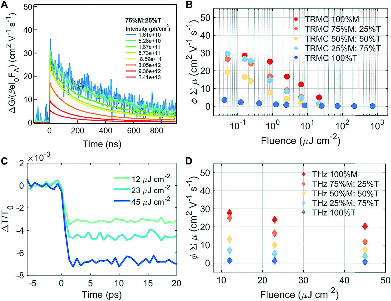 | ||
| Fig. 4 Probing the mobilities of mixed perovskites. (A) The change of photo-conductivity in TRMC as a function of time for 75% M:25% T, excited at 720 nm (excitonic peak) for different intensities. (B) The product of TRMC mobility and yield of dissociation of free charges as a function of fluences for the M–T series excited at different wavelengths (490 nm for 100% T and 720 nm for all other series). (C) The ΔT/T0 across 75% M:25% T measured on an optical-pump/terahertz-probe (THz) under different fluences (12, 23, and 45 μJ cm−2). (D) The product of THz mobility and yield of dissociation of free charges as a function of fluences (12, 23, and 45 μJ cm−2) for the M–T series. | ||
Charge carrier mobility
To understand the mobility of the 3D/LD hybrid perovskites we measured the time-resolved microwave photo-conductivity (TRMC) of the thin film series, similar to those for devices, on quartz glass. In these measurements, microwaves were used to probe the laser-induced change in conductance of the material, ΔG, as a function of time.27 A typical result is shown in Fig. 4A for a selected mixture: 75% M:25% T. The photoconductance, ΔG, increased during the pulse as charge carriers were created. After the excitation pulse, as the charge carriers recombined or became trapped, a decay in the ΔG was observed. From this measurement, we obtained the product of the yield of free charge carriers and sum of mobility, φ∑μ, from the change in photoconductance, ΔG, according to eqn (4),27,28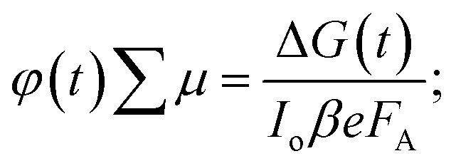 | (4) |
:25% T, 50% M:50% T, 25% M:75% T, and λ = 490 nm for 100% T, 100% D, and 100% I) varying the photon intensity, Io, from ∼109 to 1013 photons per cm2 (which corresponds to ∼1013 to 1017 carriers per cm3 for a thickness of ∼400 nm).28 These intensities were in the range of standard 1.5 AM solar illumination.29 We determined the mobility of the charge carriers from the maximum change in photoconductance, ΔGmax, as under these conditions the decay kinetics were not dominated by trapping or second order recombination. In 75% M:25% T and 3D/LD hybrid perovskites, ΔGmax was observed at intensities <∼1010 photons per cm2 (which corresponds to ∼1014 carriers per cm3 for a thickness of ∼400 nm),28 as shown in Fig. 4A. The intensity dependent measurements and half-lifetimes from TRMC measurement for all materials are shown in ESI Fig. S11–S14.†
Different photoexcitation densities/fluences affected the photoconductivity observed for the M–T series, as shown in Fig. 4B. As the photoexcitation densities were increased, the effective mobilities of 100% M and the M–T series were reduced, with the exception of 25% M:75% T. The LD sample (100% T) showed a dramatic decrease in the product of mobility and yield of dissociation of charge carriers with respect to the pure 3D and series, and exhibited no fluence dependence. The low product of mobility and dissociation of charge carriers was due to strong exciton binding energy, and they recombined very fast after the photoexcitation, and were unable to be captured using the TRMC method. The effective mobility measured in 3D 100% M was close to 30 cm2 V−1 s−1 at fluences of around 1010 to 1011 photons per cm2, as shown in ESI Fig. S1A.† This value is similar to values obtained for high quality films measured with the same experimental technique28 using THz spectroscopy.30,31 Increasing the LD content in the mixed materials yielded a drop in effective mobilities to below 30 cm2 V−1 s−1 for fluences of around 1010 to 1011 photons per cm2, as shown in Fig. 4B and S10B and C.† Slight decreases in effective mobility have been shown to affect solar cell performance dramatically, especially in terms of the hysteresis behavior.32 The improvement in hysteresis behavior was also observed in our devices, across different series, as shown in ESI Fig. S15.† However, we expected these large phase segregations, seen by XRD and absorption, which affected the photocurrents of the solar cell so severely that they also affected their mobilities. One hypothesis regarding the small changes detected for mobilities at low fluences is that for TRMC, we excited the 3D/LD perovskite samples at 720 nm, where most of the charge carriers excited in the 3D/LD mixtures come from MAPI. This is because the phase-segregated LD perovskites absorb at around 535 nm, and are not photoexcited at that particular wavelength. Therefore, only the M, 3D phase is probed.
To better understand the TRMC results, we conducted THz measurements to probe the perovskite mobilities with picosecond time scales. Transient photoconductivity measurements were performed on the same set of samples as for TRMC (the M–T series), this time excited at 400 nm to include the charge carriers excited from T, and to be able to observe the LD charge carrier mobility effects. We calculated the effective carrier mobility using an optical-pump, and we obtained the ΔT/T0 result shown in Fig. 4C and in ESI Fig. S16† for the M–T series. Carrier mobility is calculated from the peak of the conductivity at zero pump–probe delay time. The photoconductivity was highest for the 100% M sample and the conductivity reduced with increasing percentage of T, as shown in Fig. 4D. Samples with greater LD characteristics showed lower mobility.12 Similar to the TRMC result, we found that carrier mobility depended on excitation density and the lower the excitation density, the higher the effective mobility was.
The discrepancy between the TRMC and THz mobilities at the same fluences (10 to 50 μJ cm−2) can be attributed to the different time resolutions of each technique. The time resolution of TRMC is in the nanosecond regime, while that of THz is in the picosecond regime. Therefore, when measuring mobilities by TRMC, we tend to lose some of that initial signal from the first few hundred picoseconds, which can be collected by THz spectroscopy. Regardless of the absolute intensity, the effective mobility trends with respect to fluence- and composition-dependency are similar for both techniques.
Conclusions
In this study, the solar cell performance and properties of 3D/LD hybrid perovskites were studied. The addition of various LD perovskites (DMAPI, iPAPI, and tBAPI) into MAPI resulted in optical, structural, and charge carrier transport property changes, which led to changes in solar device performance. We present three important findings when mixing 3D and LD perovskites: (1) most of the additions of LD perovskites result in phase segregation of LD and 3D structures within the polycrystalline films; (2) photocurrents are massively hampered by 25% or more of the LD perovskite; and (3) the phase segregation of LD perovskites leads to reduced effective mobilities in the overall thin film. Both TRMC and THz measurements have enabled us to quantify the effective charge carrier mobilities across different photoexcitation densities and timescales. Therefore, although LD perovskites can improve environmental stability, their low effective charge carrier mobility can adversely affect solar cell performance in hybrid organic/inorganic perovskites. Hence, 3D/LD perovskite mixing must be carefully controlled when developing these types of series in solar cell devices.Experimental section
Film fabrication
For the various volume-based mixtures of 3D/LD perovskites, 4 equimolar stock solutions were prepared: methylammonium lead iodide (MAPbI3, or M), dimethylammonium lead iodide (DMAPbI3, or D), iso-propylammonium lead iodide (iPAPbI3, or I), and t-butylammonium lead iodide (tBAPbI3, or T). Initially, a 1.5 M PbI2 (Sigma-Aldrich) solution was dissolved in 9:1 DMF:DMSO mixed solvents, before mixing them with amine powder. For every gram of MAI powder (Dyesol), DMAI powder (Dyesol), iPAI powder (Dyesol), and tBAI powder (Dyesol), we added 5.10 mL, 4.67 mL, 4.25 mL, and 3.95 mL of 1.5 M PbI2 solution correspondingly. These 4 stock solutions were then mixed according to prescribed ratios.
65 μL of perovskite solution was then deposited on a pre-cleaned substrate (quartz for TRMC and THz measurement, glass slides for UV-Vis, XRD, steady-state PL, and TRPL measurements, and FTO with TiO2 for device fabrication), and spin-coated with the 2-step program: 1000 rpm for 10 s and an acceleration of 200 rpm s−1, then 6000 rpm for 30 s and an acceleration of 2000 rpm s−1. 5 seconds after the start of the second step, 200 μL of chlorobenzene was dropped on the substrate. Then, the deposited film was annealed on a hotplate at 100 °C for 10 minutes.
Single crystal growth
:1) were fully mixed in 300 μL of hydriodic acid in a 23 mL stainless steel Parr autoclave and heated at 120 °C for 3 days. The crystals were then cooled and dried under ambient conditions.
Solar cell fabrication
The etched FTO glass (Pilkington, TECS) substrates were cleaned using 2% Hellmanex in water, ethanol, and UV ozone. A TiO2 compact layer solution was made by mixing titanium diisopropoxide bis(acetylacetonate) 75% wt (Sigma-Aldrich) in ethanol (1:10 v/v ratio), and deposited using a spray pyrolysis method at 500 °C. The TiO2 mesoporous layer was prepared by mixing 1:5 w/w of TiO2 paste (SureChem, SC-HT040): solvent mix (3.5:1 w/w of terpineol:2-methoxy ethanol) and spin-coating it using a 2-step program: 500 rpm for 5 seconds, then 2500 rpm for 50 s. The substrate was then annealed at 500 °C. For the hole transport layer, we used spiro-OMeTAD (2,2′,7,7′-tetrakis-(N,N-di-p-methoxyphenyl amine)-9,9′-spirobifluorene, LumTec LT-S922). For every gram of spiro-OMeTAD, we used 227 μL of Li-TFSI (Sigma-Aldrich, 1.8 M in acetonitrile) solution, 394 μL of 4-tert-butylpyridine (Sigma-Aldrich) solution, 98 μL cobalt complex (FK209, Lumtec, 0.25 M tris(2-(1H-pyrazol-1-yl)-4-tertbutylpyridine)cobalt(III) tris(bis(trifluoromethylsulfonyl)imide) in acetonitrile) solution, and 10938 μL of chlorobenzene. 65 μL of the mixed spiro solution was deposited and spin-coated at 3000 rpm for 30 s. Finally, a 100 nm gold top electrode was deposited by thermal evaporation, with an active area of 0.16 cm2.
General characterization
The transmission and reflection for the thin film were measured using a PerkinElmer Lambda 950 UV/Vis Spectrophotometer (PerkinElmer). The method established by Tauc33 was then used to extract the bandgaps by assuming direct band gaps with an approximate film thickness of 300 nm. The crystal structure and phase of the films were characterized using an XRD (Rigaku SmartLab), with Cu-Kα sources. Pawley refinements of M–D, M–I, and M–T series compounds were performed using Highscore Plus and Topas. The film morphology and device cross-section were investigated using a Zeiss Supra 55VP field-emission scanning electron microscope (FESEM, Zeiss). J–V curves were measured using a solar simulator (Newport, Oriel Class AAA, 91195A) with a source meter (Keithley 2420) at 100 mW cm−2, AM1.5G illumination, and a calibrated Si-reference cell certified by the NREL. The J–V curves were measured at 10 mV s−1. J–V curves for all devices were measured by masking the active area with a metal mask of 0.094 cm2.Photo-conductivity measurements
Laser induced time-resolved microwave conductivity (TRMC) measurements were carried out on samples deposited on quartz substrates and placed in a sealed resonance cavity inside a nitrogen-filled glovebox. The TRMC technique measures the fractional change in microwave (8–9 GHz) power absorbed by the sample after pulsed excitation (repetition rate 10 Hz) of the thin films at their respective excitonic absorption peaks (∼720 nm for methylammonium containing samples 100% M, 75% M:25% T, 50% M:50% T, and 25% M:75% T, and ∼500 nm for LD D, I, and T). The time resolution of these measurements is limited by the width of the laser pulse (3.5 ns FWHM) and the response time of the microwave system (open cell ∼ 8 ns). Before and during the photo-conductance measurements, the samples were exposed to neither moisture nor air to prevent degradation.27,28
Optical-pump/THz-probe measurements
Charge carrier mobilities at THz frequencies were obtained by optical-pump/terahertz-probe, transient photoconductivity measurements.34 Both the optical pump pulse and THz probe pulse were generated from the same Ti:sapphire femtosecond laser amplifier (800 nm center wavelength, 2.0 mJ pulse energy, and 1 kHz repetition rate) with its output energy separated into three paths: optical pump path, THz probe path, and THz detection path. The optical pump pulses were frequency doubled to 400 nm using a beta barium borate (BBO) crystal and then focused to a 2 mm diameter at a maximum fluence of 45 μJ cm−2. The THz probe pulses (peak frequency at 1.2 THz) were generated from a two-color laser-induced gas plasma and focused to 1 mm in diameter on the sample. The arrival time differences between the pump and the probe pulses on the sample were controlled by a delay stage. We used an electro-optical sampling technique with a 1.0 mm thick 〈110〉 ZnTe crystal to detect the waveform of the THz pulse. We used lock-in techniques to record the change in THz transmission ΔT relative to its initial THz transmission T0 at the peak of the THz waveform. We calculated transient photoconductivity using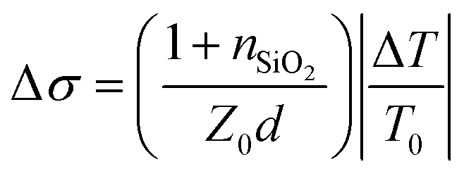 , where nSiO2 = 2.1 is the index of refraction of the quartz substrate at 1.2 THz, Z0 = 377 Ω is the impedance of free space, and d is the depth of the excited carriers (taken to be the absorption depth). Effective carrier mobility μ was further obtained from Δσ = qΔn0μ, where q is the elementary charge, and Δn0 is the initial excited carrier density. The initial excited carrier density Δn0 was taken to be ϕnphoton, with ϕ being the yield of photon-to-carrier generation and nphoton being the density of absorbed photons.
Photoluminescence measurements
Steady-state photoluminescence was recorded using a 532 nm diode laser (Thorlabs) coupled with a monochromator (Princeton Instruments, SP-300i) and an InGaAs detector (Thorlabs, DET10N). Time resolved photoluminescence lifetimes were measured using a 405 nm picosecond pulsed diode laser (Picoquant) with a repetition rate of 500 kHz using a pulse generator (Stanford Research; DG535). The laser was set to an average power of ∼10 nW using neutral density filters and focused to a 150 μm spot on the perovskite film. The emission from the film was collected and collimated using an off-axis parabolic mirror (Thorlabs, MPD269V) and sent into a silicon single photon counting detector (PerkinElmer, SPCM-AQR-13). Scattered laser excitation was suppressed using a 405 nm notch filter and a 420 nm longpass filter. Photon arrival times were recorded using a time-correlated single photon counting card (Picoquant, PicoHarp 300).Conflicts of interest
There are no conflicts to declare.Acknowledgements
NTPH, SS, TB, and JPCB are supported by the NSF grant CBET-1605495. JPCB is supported by the DOE EERE Postdoctoral Research Award. JY is funded by the Institute for Soldier Nanotechnology (ISN) grant W911NF-13-D-0001 and by the National Aeronautics and Space Administration (NASA) grant NNX16AM70H. FW is funded by the Accelerated Materials Development for Manufacturing from IMRE, A*STAR, grant number A1898b0043. M-JS, PJP, and MPE are supported by Wesleyan College of the Environment Faculty-Led Research Project Grants. MCGR and FCG are supported by funding from the European Research Council Horizon 2020 ERC Grant Agreement no. 648433.References
- J.-P. Correa-Baena, M. Saliba and T. Buonassisi, et al., Promises and challenges of perovskite solar cells, Science, 2017, 358(6364), 739–744, DOI:10.1126/science.aam6323.
- National Renewable Energy Laboratory, Best Research-Cell Efficiencies, 2019, https://www.nrel.gov/pv/assets/pdfs/best-research-cell-efficiencies-190416.pdf, accessed May 13, 2019 Search PubMed.
- G. Niu, X. Guo and L. Wang, Review of recent progress in chemical stability of perovskite solar cells, J. Mater. Chem. A, 2015, 3(17), 8970–8980, 10.1039/c4ta04994b.
- I. C. Smith, E. T. Hoke, D. Solis-Ibarra, M. D. McGehee and H. I. Karunadasa, A Layered Hybrid Perovskite Solar-Cell Absorber with Enhanced Moisture Stability, Angew. Chem., Int. Ed., 2014, 53(42), 11232–11235, DOI:10.1002/anie.201406466.
- D. S. Lee, J. S. Yun and J. Kim, et al., Passivation of Grain Boundaries by Phenethylammonium in Formamidinium–Methylammonium Lead Halide Perovskite Solar Cells, ACS Energy Lett., 2018, 3(3), 647–654, DOI:10.1021/acsenergylett.8b00121.
- L. N. Quan, M. Yuan and R. Comin, et al., Ligand-Stabilized Reduced-Dimensionality Perovskites, J. Am. Chem. Soc., 2016, 138(8), 2649–2655, DOI:10.1021/jacs.5b11740.
- D. H. Cao, C. C. Stoumpos and T. Yokoyama, et al., Thin Films and Solar Cells Based on Semiconducting Two-Dimensional Ruddlesden–Popper (CH3(CH2)3NH3)2(CH3NH3)n−1SnnI3n+1 Pe, ACS Energy Lett., 2017, 2(5), 982–990, DOI:10.1021/acsenergylett.7b00202.
- J.-F. Liao, H.-S. Rao, B.-X. Chen, D.-B. Kuang and C.-Y. Su, Dimension engineering on cesium lead iodide for efficient and stable perovskite solar cells, J. Mater. Chem. A, 2017, 5(5), 2066–2072, 10.1039/c6ta09582h.
- T. Zhang, M. I. Dar and G. Li, et al., Bication lead iodide 2D perovskite component to stabilize inorganic α-CsPbI3 perovskite phase for high-efficiency solar cells, Sci. Adv., 2017, 3(9), e1700841, DOI:10.1126/sciadv.1700841.
- G. Liu, H. Zheng, X. Xu, L.-Z. Zhu, X. Zhang and X. Pan, Design of High-Efficiency and Environmentally Stable Mixed-Dimensional Perovskite Solar Cells Based on Cesium–Formamidinium Lead Halide Component, Chem. Mater., 2018, 30(21), 7691–7698, DOI:10.1021/acs.chemmater.8b02970.
- D. H. Cao, C. C. Stoumpos, O. K. Farha, J. T. Hupp and M. G. Kanatzidis, 2D Homologous Perovskites as Light-Absorbing Materials for Solar Cell Applications, J. Am. Chem. Soc., 2015, 137(24), 7843–7850, DOI:10.1021/jacs.5b03796.
- R. L. Milot, R. J. Sutton and G. E. Eperon, et al., Charge-Carrier Dynamics in 2D Hybrid Metal-Halide Perovskites, Nano Lett., 2016, 16(11), 7001–7007, DOI:10.1021/acs.nanolett.6b03114.
- A. Z. Chen, M. Shiu and J. H. Ma, et al., Origin of vertical orientation in two-dimensional metal halide perovskites and its effect on photovoltaic performance, Nat. Commun., 2018, 9(1), 1336, DOI:10.1038/s41467-018-03757-0.
- S. D. Stranks, G. E. Eperon and G. Grancini, et al., Electron–hole diffusion lengths exceeding 1 micrometer in an organometal trihalide perovskite absorber, Science, 2013, 342(6156), 341–344, DOI:10.1126/science.1243982.
- A. H. Slavney, T. Hu, A. M. Lindenberg and H. I. Karunadasa, A Bismuth-Halide Double Perovskite with Long Carrier Recombination Lifetime for Photovoltaic Applications, J. Am. Chem. Soc., 2016, 138(7), 2138–2141, DOI:10.1021/jacs.5b13294.
- J.-P. Correa-Baena, L. Nienhaus and R. C. Kurchin, et al., A-Site Cation in Inorganic A3Sb2I9 Perovskite Influences Structural Dimensionality, Exciton Binding Energy, and Solar Cell Performance, Chem. Mater., 2018, 30(11), 3734–3742, DOI:10.1021/acs.chemmater.8b00676.
- R. E. Brandt, J. R. Poindexter and P. Gorai, et al., Searching for “Defect-Tolerant” Photovoltaic Materials: Combined Theoretical and Experimental Screening, Chem. Mater., 2017, 29(11), 4667–4674, DOI:10.1021/acs.chemmater.6b05496.
- F. Brivio, J. M. Frost and J. M. Skelton, et al., Lattice dynamics and vibrational spectra of the orthorhombic, tetragonal, and cubic phases of methylammonium lead iodide, Phys. Rev. B: Condens. Matter Mater. Phys., 2015, 92(14), 144308, DOI:10.1103/PhysRevB.92.144308.
- G. Kieslich, S. Sun and A. K. Cheetham, Solid-state principles applied to organic–inorganic perovskites: new tricks for an old dog, Chem. Sci., 2014, 5(12), 4712–4715, 10.1039/c4sc02211d.
- M. Becker, T. Klüner and M. Wark, Formation of hybrid ABX3 perovskite compounds for solar cell application: first-principles calculations of effective ionic radii and determination of tolerance factors, Dalton Trans., 2017, 46(11), 3500–3509, 10.1039/c6dt04796c.
- S. F. Hoefler, G. Trimmel and T. Rath, Progress on lead-free metal halide perovskites for photovoltaic applications: a review, Monatsh. Chem. Chem. Mon., 2017, 148(5), 795–826, DOI:10.1007/s00706-017-1933-9.
- C.-M. Hsieh, Y.-L. Yu, C.-P. Chen and S.-C. Chuang, Effects of the additives n-propylammonium or n-butylammonium iodide on the performance of perovskite solar cells, RSC Adv., 2017, 7(88), 55986–55992, 10.1039/c7ra11286f.
- M. Saliba, J.-P. Correa-Baena and C. M. Wolff, et al., How to Make over 20% Efficient Perovskite Solar Cells in Regular (n–i–p) and Inverted (p–i–n) Architectures, Chem. Mater., 2018, 30(13), 4193–4201, DOI:10.1021/acs.chemmater.8b00136.
- D. Bi, W. Tress and M. I. Dar, et al., Efficient luminescent solar cells based on tailored mixed-cation perovskites, Sci. Adv., 2016, 2(1), e1501170, DOI:10.1126/sciadv.1501170.
- C. Roldán-Carmona, P. Gratia and I. Zimmermann, et al., High efficiency methylammonium lead triiodide perovskite solar cells: the relevance of non-stoichiometric precursors, Energy Environ. Sci., 2015, 8(12), 3550–3556, 10.1039/c5ee02555a.
- J.-C. Blancon, H. Tsai and W. Nie, et al., Extremely efficient internal exciton dissociation through edge states in layered 2D perovskites, Science, 2017, 355(6331), 1288–1292, DOI:10.1126/science.aal4211.
- T. J. Savenije, A. J. Ferguson, N. Kopidakis and G. Rumbles, Revealing the Dynamics of Charge Carriers in Polymer:Fullerene Blends Using Photoinduced Time-Resolved Microwave Conductivity, J. Phys. Chem. C, 2013, 117(46), 24085–24103, DOI:10.1021/jp406706u.
- E. M. Hutter, G. E. Eperon, S. D. Stranks and T. J. Savenije, Charge Carriers in Planar and Meso-Structured Organic–Inorganic Perovskites: Mobilities, Lifetimes, and Concentrations of Trap States, J. Phys. Chem. Lett., 2015, 6(15), 3082–3090, DOI:10.1021/acs.jpclett.5b01361.
- C.-S. Jiang, M. Yang and Y. Zhou, et al., Carrier separation and transport in perovskite solar cells studied by nanometre-scale profiling of electrical potential, Nat. Commun., 2015, 6(1), 8397, DOI:10.1038/ncomms9397.
- G. E. Eperon, V. M. Burlakov, P. Docampo, A. Goriely and H. J. Snaith, Morphological Control for High Performance, Solution-Processed Planar Heterojunction Perovskite Solar Cells, Adv. Funct. Mater., 2014, 24(1), 151–157, DOI:10.1002/adfm.201302090.
- R. L. Milot, G. E. Eperon, H. J. Snaith, M. B. Johnston and L. M. Herz, Temperature-Dependent Charge-Carrier Dynamics in CH3NH3PbI3 Perovskite Thin Films, Adv. Funct. Mater., 2015, 25(39), 6218–6227, DOI:10.1002/adfm.201502340.
- S. H. Turren-Cruz, M. Saliba and M. T. Mayer, et al., Enhanced charge carrier mobility and lifetime suppress hysteresis and improve efficiency in planar perovskite solar cells, Energy Environ. Sci., 2018, 11(1), 78–86, 10.1039/c7ee02901b.
- J. Tauc, Optical properties and electronic structure of amorphous Ge and Si, Mater. Res. Bull., 1968, 3(1), 37–46, DOI:10.1016/0025-5408(68)90023-8.
- M.-J. Sher, C. B. Simmons and J. J. Krich, et al., Picosecond carrier recombination dynamics in chalcogen-hyperdoped silicon, Appl. Phys. Lett., 2014, 105(5), 053905, DOI:10.1063/1.4892357.
Footnote |
| † Electronic supplementary information (ESI) available. See DOI: 10.1039/c9ta05241k |
| This journal is © The Royal Society of Chemistry 2019 |