
 Open Access Article
 This Open Access Article is licensed under a Creative Commons Attribution-Non Commercial 3.0 Unported Licence
Photocatalytic hydrogen evolution activity of Co/CoO hybrid structures: a first-principles study on the Co layer thickness effect†
Kyoung-Won
Park
 ab and
Alexie M.
Kolpak
*c
ab and
Alexie M.
Kolpak
*c
aDepartment of Materials Science and Engineering, Massachusetts Institute of Technology, Cambridge, Massachusetts 02139, USA
bCenter for Biomaterials, Korea Institute of Science and Technology (KIST), Seoul, 02792, Republic of Korea
cDepartment of Mechanical Engineering, Massachusetts Institute of Technology, Cambridge, Massachusetts 02139, USA. E-mail: alexie.kolpak@gmail.com
First published on 5th June 2019
Abstract
Both metal and semiconductor nanoparticles can induce water splitting in response to light but in different ways: metal nanoparticles can generate hot carriers with a surface plasmon resonance (SPR) effect and semiconductor nanoparticles with optimal band gap and band edges are light absorbers for hydrogen and oxygen evolution reactions (HER and OER). Hence, hybrid structures of metals and semiconductors have been anticipated to have enhanced photocatalytic activities compared to pure metals and semiconductors. To find an optimal hybrid structure for the photocatalytic HER in water splitting, we herein construct Co/CoO hybrid structures with variation of the Co layer thickness, using density functional theory (DFT) calculations. It is found that the Co/CoO hybrid structures have different electronic characteristics with respect to the Co layer thickness, which leads to the varied photocatalytic activities. Based on this study, we find out the optimal Co layer thickness for the highest HER activity. For the SPR effect, a thick enough Co layer is necessary, while a thin enough Co layer is required for optimal light absorption for the HER in solar-driven water splitting. We believe that this thorough study on the photo-responses occurring in Co/CoO heterojunction systems can be considered as a framework to design new photocatalytic metal/semiconductor heterojunction systems with first-principles studies.
Introduction
Spontaneous solar-driven water splitting is a highly promising pathway for clean and renewable energy supply in the future. The ultimate goal is to develop efficient, economical and stable photocatalysts which are able to accomplish overall water splitting under visible light irradiation, without using a sacrificial agent or external bias. Recently, cobalt-based materials have been highlighted as innovative solar-driven water splitting catalysts. This is because of their H2 evolving ability,1,2 different from most cobalt-based materials which have been assessed as water oxidizing electrocatalysts in the past decade.3–10 To date, CoO nanoparticles showed a high solar-to-hydrogen conversion efficiency producing both H2 and O2 without external bias or a co-catalyst in neutral water.11 The overall water splitting on CoO nanoparticles could be realized because three steps of photocatalysis12 occurred spontaneously under illumination: (i) a specific facet on the CoO nanoparticles has optimal band edge positions relative to the water redox potential for overall water splitting by light absorption,13 (ii) the photogenerated charge carriers are efficiently separated between two different kinds of facets on the nanoparticles,14 and (iii) the charge carriers photogenerated on the nanoparticles have high enough energies to overcome the kinetic barriers for H2 and O2 evolution at the active facets.14 However, for a monolithic nanoparticle, this spontaneous photocatalysis is observed under very limited conditions of specific material, morphology, size and surface environment.11,13–23In general, metal co-catalysts have often been deposited on semiconducting photocatalysts to promote the HER activity for two reasons: metal co-catalysts can separate charge carriers by suppressing the electron–hole recombination in photocatalysts and serve as the reaction sites by lowering the kinetic barrier for the HER. Metal Co formed on CoO nanoparticles with simple annealing in a reducing environment also lowered the kinetic barrier for the HER (HER overpotential) and improved the electrochemical HER activity compared to pure CoO.24 The enhancement in the HER activity was dependent on the thickness of the Co layer formed in the Co/CoO hybrid structures.24 In particular, an optimal Co layer thickness in the Co/CoO hybrid structure exhibited a very low HER overpotential comparable to that of the commercial Pt/C catalyst, together with much better long-term stability than pure CoO.24 Nevertheless, the origins of the enhancement and the thickness dependency of the HER activity have not been clarified yet. Furthermore, it has not been studied whether the Co/CoO hybrid structures are photocatalytically active for hydrogen evolution from water splitting.
In our previous study,13 it was suggested that the photocatalytic capability of CoO for the HER can be improved with metal Co decoration. Co decoration shifts the band edges of the CoO layer to a more negative potential relative to the H+/H2 level, different from those of the bare CoO surface with a positive potential,13 suggesting that Co decoration makes the CoO layer active for H2 evolution under irradiation. In addition to the photo-response of the semiconducting CoO layer, metal Co itself can induce the surface plasmon resonance (SPR) effect.25 This SPR effect occurs when metal nanoparticles with a size much smaller than the photon wavelength excite surface plasmons under illumination, and create electron–hole pairs of high energy called hot electron–holes. The SPR effect can be employed to deliver hot carriers from the metal nanoparticle to the adjacent semiconducting (or insulating) substrate and to induce the HER/OER on the hybrid structure from water splitting.26–28 This effect is very important and interesting in the photocatalysis of water, since it can trigger the HER/OER even with large band gap materials (of the UV spectrum) under visible light, with the hot carriers transferred from metal nanostructures.
We herein study the photocatalytic behaviors of the Co/CoO hybrid structures with different Co layer thicknesses for H2 evolution. The thickness-dependent interfacial structures/properties of the Co/CoO hybrid structures are identified by examining the electron transfer between the Co and CoO layers, band bending aspects in CoO layers and Schottky barrier height (SBH). We also investigate the two kinds of photo-responses occurring in metal Co and semiconducting CoO layers as a function of the Co layer thickness, independently: to evaluate the feasibility of the photocatalytic HER on the Co/CoO hybrid structures by light absorption by CoO, we compare the conduction band edge position (EC) relative to the water reduction potential level (H+/H2), with the HER overpotential. For the investigation of the SPR effect in Co layers, the distribution of energy-population of hot electrons is calculated. Based on the thickness-dependent photocatalytic properties, we determine the optimal thickness of the Co layer in the hybrid structures for active H2 evolution from water splitting under visible light sources.
Methods
Co/CoO(111) structure
Co/CoO core–shell structured nanoparticles are experimentally manufactured by reducing CoO nanoparticles in a pure Ar or Ar/H2 mixture atmosphere.24 The interface of the Co and CoO regions formed during the reducing procedure showed smooth (111) plane matching between the Co and CoO layers.24 To mimic the Co layers and interface in the Co/CoO core–shell structure experimentally generated, we removed 1–4 oxygen atomic layers from both surface sides of the initial CoO(111) lattices. The created hybrid structure has a Co layer (face-centered cubic (FCC) structure) in the shell and a CoO layer in the core with a symmetric supercell as shown in Fig. S1 in the ESI† as an example. To study the sole effect of the Co layer thickness, the total number of CoO layers was fixed at 5 Co and 4 O layers. We named each supercell Co(x)/CoO(111), where x is the number of atomic Co(111) layers formed on the CoO(111) core. For example, Co(4)/CoO(111) denotes a hybrid structure which has 4 atomic Co(111) layers on each shell layer in a symmetric supercell, together with a CoO(111) layer in the central region.We modeled Co/CoO(111) slabs using supercells of a (2 × 2) in-plane unit cell with 4 atoms in each layer (Fig. S1 in the ESI†). For the structural relaxations of the slabs, a vacuum layer of ∼15 Å was constructed perpendicular to the surface. The atoms in the central 5 atomic layers were fixed in the bulk CoO positions, while all other atoms were allowed to fully relax. A type-II antiferromagnetic (AFM-II) spin ordering was initially set in all slab structures in which the magnetic moments of the Co2+ ions are ferromagnetic within each (111) plane, with antiparallel ordering of adjacent (111) planes.13,29–31 To address the strongly correlated and localized 3d shell of Co, we employed the DFT + Hubbard U (DFT + U) approach within spin-polarized density functional theory using VASP.32,33Ueff = 4.1 eV on Co atoms was applied since the Ueff correction gives a lattice constant, magnetic moment, and band gap of CoO in good agreement with the experimental values.13 Projected augmented wave (PAW) pseudopotentials from the VASP database and the generalized gradient approximation (GGA) of Perdew–Burke–Ernzerhof (PBE) were used to describe the exchange-correlation effects.34 An energy cutoff of 800 eV, a 6 × 6 × 1 Monkhorst–Pack k-point mesh, and a Gaussian smearing width of 0.05 eV were used. Atom positions were relaxed until all forces were less than 0.005 eV Å−1.
Prediction of ECvs. H+/H2
Previous studies on band edge position calculations of CoO surfaces with a vacuum layer13 have been unable to reproduce their band edge positions experimentally observed in an aqueous solution. Unlike the vacuum calculation or the implicit solvation calculation of CoO, an explicit solvation method with direct contact of bulk liquid water could reproduce the band edge positions experimentally measured in an aqueous solution.13 Therefore, in this study, to predict the conduction band edge position relative to the water reduction potential level (ECvs. E (H+/H2)) of the CoO(111) layers in the Co/CoO(111) hybrid structures in an aqueous environment, three step calculations of an explicit solvation method are conducted as introduced in ref. 13,35, and 36:| Eint,CoOCvs. E(H+/H2) = (ECoOC − HCoO) − (AH2O − HH2O) + (Hint,CoO−Hint,H2O), | (1) |
For the potential drop at the interface (third term in eqn (1), Hint,CoO − Hint,H2O), liquid water/Co/CoO(111) interfaces were explicitly constructed with direct contact of the DFT-relaxed Co/CoO(111) slabs and the bulk liquid water prepared with classical molecular dynamics (MD) simulations.13 The Hartree potentials of the water/Co/CoO interfaces were obtained as a function of the position from the bottom of the Co/CoO(111) slab to bulk liquid water, with static DFT calculations (Fig. S2 in the ESI†). For the static DFT calculations, we ignored both spin polarization of the Co atoms and Hubbard U correction. This is because water contact makes the CoO surface lose considerable magnetic moment of Co atoms (Fig. S4–S7† in ref. 13) and weakens the localization of the 3d-band of Co atoms (Fig. S8† in ref. 13). The detailed reason for the ignorance of spin polarization and the Hubbard U correction in the explicit solvation method is explained in ref. 13 and 36.
HER overpotential
We determined the thermodynamic stability of H adsorbed (intrinsic barriers for the HER) on the Co/CoO(111) surfaces by calculating the free energy change for hydrogen adsorption (ΔGH*), which has shown to be a good HER activity descriptor for a wide variety of surfaces.37,38 The ΔGH* can be computed by modeling the possible intermediates formed during the hydrogen adsorption–reduction–desorption processes at the cathode, given by 2H+ + 2e− → H* + H+ + e− → H2.Free energy changes (ΔG) for the intermediates at PH2 = 1 bar were calculated using the approach reported in ref. 39, where
| ΔG(U,pH,T) = ΔE + ΔZPE − TΔS + ΔGU + ΔGpH, | (2) |
![[thin space (1/6-em)]](https://www.rsc.org/images/entities/char_2009.gif) 10 × pH is the free energy change due to the change in pH. All values of ΔG are computed at T = 298 K and pH = 1.
10 × pH is the free energy change due to the change in pH. All values of ΔG are computed at T = 298 K and pH = 1.
Hot electron energy distribution
The energy distribution of the hot carriers immediately after photon absorption is determined from the initial states of electrons in the Fermi gas and the incident photon energy (Eph). We estimated the energy-population distribution of the hot electrons created in Co layers, with the transition probability (P(E) in eqn (3) which describes the joint density of states multiplied by their respective Fermi distribution functions, f(E)), as introduced in ref. 40.| P(E) ∝ D(E − Eph)f(E − Eph)D(E)(1 − f(E)), | (3) |
For the prediction of hot electron energy-probability distribution in the ferromagnetic (FM) Co layer, it is assumed that spin flipping is available at the moment of the transition when the incident light resonates with the Co layer.
Results and discussion
Structures of Co layers
It has been widely believed that the characteristics of a heterointerface formed with two different materials are determined by the bulk characteristics of the two materials. Undoubtedly, a phase located far away from the heterointerface will have a structure similar to its bulk phase. Yet, a variety of interesting and unexpected phenomena have been found to originate from the peculiar heterointerfaces in many systems.41–45 The peculiar heterointerfaces might come from the interesting combination of two different materials, or from a heterointerfacial structure/property different from that of their bulk phases. In the case of an epitaxial interface, the structures/properties are more complex because various effects come from lattice mismatch (strain) between the adjacent materials.A recent HRTEM (high resolution transmission electron microscopy) image showed that a Co/CoO core–shell hybrid structure prepared by reducing CoO nanoparticles has a smooth lattice matching along the (111) plane at the interface of the Co and CoO layers.24 The lattice parameter of the Co layer is the same as that of the adjacent CoO lattice (∼0.24 nm), which is largely different from the bulk value of the central Co core (∼0.2 nm). This directly shows that the Co layer right next to the Co/CoO interface is epitaxial with the CoO layer, and the Co layer is subjected to very large in-plane strain, up to 20% tension.
In general, the very large strain due to lattice mismatch at the interface is accompanied by the structural defect formation for relaxing the strain, but some HRTEM observations of metal/metal oxide heterojunction systems46–51 manipulated with oxidation (or reduction) exhibited high porosity together with an epitaxial metal/metal oxide interface, without the formation of other defects. Even for the Co/CoO(100) interface created from the oxidation of Co, an epitaxial structure is formed without defect formation at the interface,46–51 but with high porosity52 as observed at the Co/CoO(111) interface.24 Therefore, the formation of an epitaxial heterointerface in the Co/CoO(111) hybrid structure might be feasible in the very localized region with the assistance of the enormous pores for strain relaxation, although we have not been able to imagine the epitaxial structure owing to the very large lattice mismatch between metal and oxide layers.
Fig. 1(a) shows the atomic configurations of the DFT-relaxed Co/CoO(111) hybrid structures constructed from the removal of oxygen from the initial CoO(111) lattice. The relaxed structures describe the Co/CoO(111) shell/core structures which have CoO(111) in the core and Co(111) in the shell regions. All hybrid structures seem to have epitaxial structures with the CoO layers underneath as observed experimentally.24 Thus, all Co layers have almost 20% tensile strain along the in-plane axis, as expected from a previous HRTEM image.24 According to our MD studies (effects of the defects (Fig. S3 in the ESI†), aspect ratio (Fig. S4–S6 in the ESI†) and size (Fig. S7 in the ESI†) on the stress–strain curves of Co), a thin film of a perfect lattice without defects with a low aspect ratio and small size can have considerably improved elastic limit (elasticity) compared to the bulk metal. These conditions are similar to the Co thin layer in the Co/CoO core/shell nanoparticles. Also, it was experimentally confirmed that the elastic limit and yield strength of Au nanowires53 and sub-micron metallic glasses54 significantly increase by ∼3 to 10 times compared to their bulk phases. Hence, the metal Co layer formed on CoO nanoparticles may sustain the large lattice mismatch in the local area without generating defects.
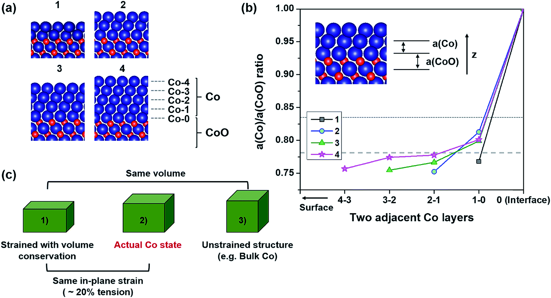 | ||
| Fig. 1 (a) Atomic configurations of Co(x)/CoO(111) hybrid structures constructed with different numbers of Co layers, x. Blue and red circles are Co and O atoms, respectively. The number above each figure denotes x in Co(x)/CoO(111). Each atomic Co layer is named Co-n from the interfacial Co layer (Co-0) to the surface Co layer (Co-x) in Co(x)/CoO(111). (b) Lattice parameter ratio of Co and CoO layers along the thickness axis as defined in the inset. The number in the legend is x in Co(x)/CoO(111). The horizontal axis is about two adjacent Co layers, for example, 4-3 denotes two adjacent Co-3 and Co-4 layers as named in (a). The two horizontal dotted lines denote the middle and upper ideal values (0.782 and 0.833). The lattice parameter of the CoO layer is obtained from the central region of the symmetric supercell. (c) A schematic showing the actual Co structural state between two ideal structural states: 20% tensile strained structure along the in-plane direction with volume conservation and the unstrained structure the same as bulk FCC-Co. | ||
In addition to the severe in-plane strain in Co layers, to identify their structures along the out-of-plane axis, we investigate the lattice parameter ratio of Co and CoO layers (a(Co)/a(CoO) ratio) along the thickness direction as defined in the inset of Fig. 1(b). There are three ideal values for the a(Co)/a(CoO) ratio in this study. One is 0.579, when volume is conserved even under a large in-plane strain of 20% (lower ideal value), which is an unrealistic case. The second is 0.782, when face-centered cubic (FCC) structured-Co follows Poisson's ratio of Co = 0.31 (ref. 55) under elastic in-plane strain (middle ideal value). The final is the bulk value, i.e., 0.833, when the Co layer is unstrained (upper ideal value). As can be seen in Fig. 1(b), all the ratios in the Co/CoO(111) hybrid structures are between the lower and upper ideal values, and very close to the middle value. This means that the actual structural state of the interfacial Co layers is similar to that of the biaxially strained Co following its Poisson's ratio. Therefore, the Co layers are present between the two ideal states as schematically depicted in Fig. 1(c), which suggests that the Co layers experience a volume expansion of ∼31.33% compared to the bulk phase, under 20% tension along the in-plane direction.
Each Co layer in the hybrid structure has a slightly different a(Co)/a(CoO) ratio depending on the position and thickness. Co layers have lower a(Co)/a(CoO) ratios going from the interface to the surface layer. This means that surface Co layers tend to have a slightly denser structure, while interfacial Co layers form a looser structure, relatively. The central region of Co layers (neither surface nor interfacial layer) in Co(4)/CoO(111), exhibits a similar ratio to the middle ideal value, which shows that thicker Co layers have the strained structure of bulk Co in the center. These thickness-dependent structures of Co layers are expected to result in different interfacial properties and different photocatalytic behaviors in the Co(x)/CoO(111) structures, as observed in the examination of other properties.41,48,49,52,56–66
Work function of Co/CoO(111)
When a metal and a semiconductor are brought into contact, atoms and electrons are redistributed at the interface until the equilibration of the electrochemical potential is achieved. The equilibration process is accompanied by electron transfer across the interface, which results in the formation of a space charge layer in the semiconductor at the interface. As a result, the conduction and valence band edges at the interface deviate from their bulk values, which in turn bends the energy bands of the semiconductor and forms the SBH for charge transfer (ϕe for electron and ϕh for hole).The degree/direction of band bending and the SBH formed at the interface have long been commonly correlated with work functions (Φ) of the two different materials because the amount/direction of electron transfer is characterized by the relative electron affinities of their bulk phases; a material of high work function strongly attracts electrons and vice versa. However, the band bending aspects and SBH frequently deviate from the prediction with work functions of bulk phases since the work functions of materials are influenced by the surface state, e.g., surface orientation, adsorbates and thickness.67,68
Fig. 2(a) shows the change in work functions of the Co/CoO(111) hybrid structures with variation of the Co layer thickness in the structure. For comparison, work functions of isolated and undeformed Co(111) and CoO(111) slabs (named ‘IU-Co’ and ‘IU-CoO’) with different thicknesses are shown in Fig. 2(b). The work function of the entire Co/CoO hybrid structure (blue square in Fig. 2(a)) decreases up to Co(2)/CoO(111) from the bare CoO(111) slab, and it increases again beyond the critical thickness of the Co layer. This demonstrates that even though the same materials (Co and CoO in this study) form the heterointerface, the created interface has different electron affinities depending on the relative thickness of the two materials, which deviates from the prediction with work functions of their bulk phases.69 In addition, the work function of Co(111) layers isolated from the hybrid structure (named ‘I-Co’, red triangle in Fig. 2(a)) also slightly decreases up to 2 atomic Co layers, followed by an increase beyond the critical thickness. The variation in work function of the 1–2 layered I-Co slabs does not follow the trend of the IU-Co slabs which monotonically increases with increasing Co thickness. In contrast, the variation of the 2–4 layered I-Co slabs seems to trace the change in the IU-Co slabs (green diamond in Fig. 2(b)). This is because the work function of Co slabs is sensitive to strain, the magnitude of which is also dependent on the Co layer thickness (Fig. S8 in the ESI†). Also, a slightly reduced work function in the I-Co slabs than in the IU-Co slabs seems to be related to the tensile strain exerted on I-Co at the interface, since tensile strain decreases the work function of the FCC-Co(111) slabs (Fig. S9 in the ESI†).
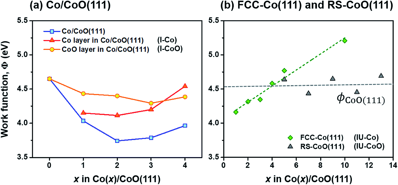 | ||
| Fig. 2 Work functions of (a) Co/CoO(111) hybrid structures as a function of the number of Co layers, (b) isolated and undeformed FCC-Co(111) and RS-CoO(111) slabs (IU-Co and IU-CoO) as a function of the number of layers. In figure (a), work functions of Co and CoO layers isolated from each hybrid structure are superimposed on the figure (denoted as ‘I-Co’ and ‘I-CoO’). The variation in work functions of IU-Co and IU-CoO is extrapolated by ΦCo(111) = 0.118 × # of Co layer + 4.073 (green dashed line) and ΦCoO(111) = 0.0062 × # of CoO layer + 4.517 (gray dashed line) in figure (b). The cross point of green and gray lines in figure (b) is ∼3.98. | ||
A close look at Fig. 2 provides an interesting point that there is a cross point between the work functions of Co and CoO layers, around 3 or 4 Co layers both in I-Co/I-CoO (Fig. 2(a)) and in IU-Co/IU-CoO (Fig. 2(b)). This suggests that the relative electron affinities of Co and CoO layers suddenly become the opposite around the critical Co layer thickness; consequently, the direction of electron transfer becomes the other direction. That is, the variation of the Co layer thickness can simply modulate the electronic characteristics of the Co/CoO(111) interface. This modulation is unavailable with the change of CoO layer thickness, because the work function of IU-CoO slabs scarcely changes with respect to thickness (gray triangle in Fig. 2(b)). Therefore, changing the work function of the Co layer with thickness, as we do in this study, is suitable to control the interfacial electronic structure of the Co/CoO core–shell structure.
SBH and band bending
In this section, to confirm the predicted change in the interfacial electronic characteristics at around 3–4 Co layers, we examine SBHs for electrons and holes (ϕe and ϕh), charge transfer at the Co/CoO(111) interface and band bending in the CoO(111) layers. Fig. 3(b) shows an example of the local density of states (LDOS) of each Co and CoO layer in the Co(1)/CoO (111) hybrid structure as denoted in the atomic configuration of the structure (Fig. 3(a)). The interface of the Co/CoO(111) structure presents metallic behavior, since there is no energy gap in the DOS. The central region of CoO(111) has a band gap of ∼2.6 eV between the conduction and valence band edges, which is in good agreement with the band gap of bulk RS-structured CoO.32,70–72ϕe (or ϕh) is measured from the energy difference between the Fermi level (EF) of the Co/CoO(111) structure and the EC (or EV), as shown in Fig. 3(b). The ϕe (or ϕh) gradually increases (decreases) with increasing thickness of the Co layer. This shows that as the Co layer becomes thicker, electron transfer from Co to CoO becomes less probable, while hole transfer becomes easier. Between 3 and 4 Co layers, the sign of ϕh suddenly becomes the opposite, suggesting the absence of a barrier for hole transfer, that is, the formation of ohmic contact between the Co and CoO layers.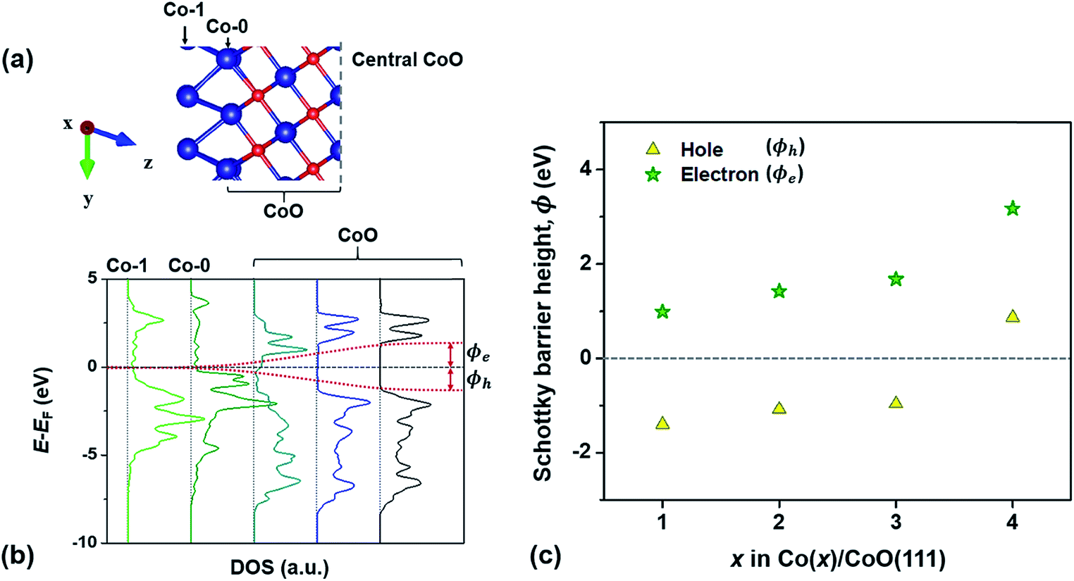 | ||
| Fig. 3 Examples of (a) atomic configuration of the Co(1)/CoO(111) structure and (b) local density of states (LDOS) of Co and CoO layers in the Co(1)/CoO(111) structure with respect to E − EF. (c) Schottky barrier heights (SBHs) for electrons and holes in Co(x)/CoO(111) hybrid structures with different numbers of Co layers, x. ϕe and ϕh in figures (b) and (c) indicate SBHs for electrons and holes. | ||
Since the space charge layer width (10 nm to several μm) is larger than the CoO thickness (the size of the Co/CoO(111) core–shell observed in experiment24 is about 10 nm in diameter), the band bending effect is ignorable in the CoO layer in the Co/CoO core–shell nanoparticles. But, to understand charge transfer behavior between metallic Co and semiconducting CoO layers in the process of electrochemical potential equilibration of the two phases, we predict intrinsic band bending to occur in the CoO layers by drawing the EC and EV at the interface with respect to those of the bulk CoO phase,73,74 as shown in Fig. 4. The band bending is downward in the hybrid structures with 1–3 Co layers, the degree of which decreases with increasing Co layer thickness. Yet it suddenly becomes upward in the Co(4)/CoO(111) structure. These thickness-dependent band bending aspects stem from the thickness-dependent electron affinity of the Co layer relative to that of the CoO layers in the hybrid structure: ΦCo is smaller than ΦCoO in the hybrid structures with 1–3 Co layers, whereas it is greater in Co than in CoO in the Co(4)/CoO(111) structure, i.e., ΦCo > ΦCoO, as predicted in Fig. 2(a). These band bending aspects provide important information that electrons transfer from Co to CoO in the hybrid structures with 1–3 Co layers in the electrochemical potential equilibrium process, while electrons are collected from CoO to Co in the Co(4)/CoO(111) structure. Upward band bending occurs from the Co(4)/CoO(111) structure to the thicker Co layer decorated hybrid structure (more than 4 atomic Co layers, i.e., for a thick enough Co layer), as expected from work functions of bulk Co and CoO phases: Co attracts electrons more strongly than CoO, and electrons are depleted in the CoO layer near the interface, resulting in upward band bending.
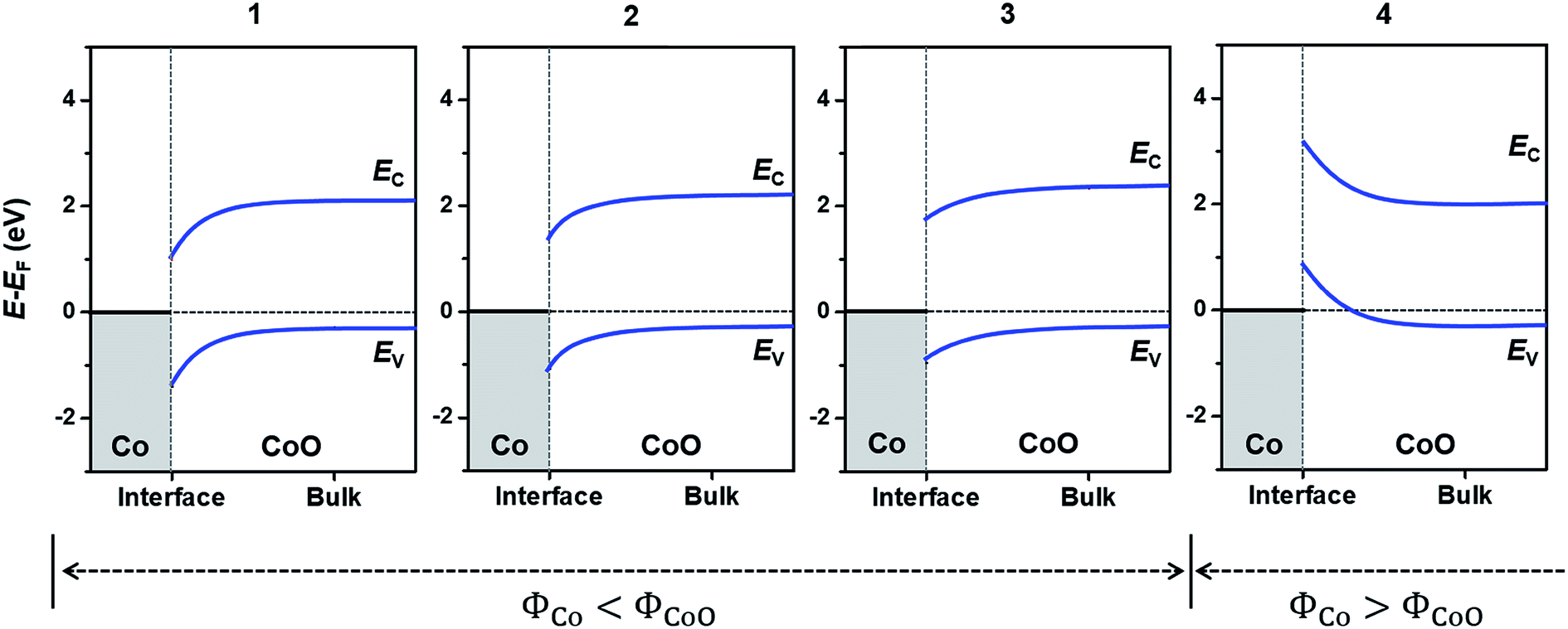 | ||
| Fig. 4 Band bending in Co(x)/CoO(111) hybrid structures with respect to bulk CoO, with different Co layer thicknesses, x. The number at the top of each graph denotes x in the Co(x)/CoO(111) structures. The conduction and valence band edges (EC and EV) of bulk CoO are determined by the experimentally observed value; the Fermi level is ∼0.3 eV above the EV.73,74 The horizontal gray dashed line denotes the EF of each Co/CoO(111) structure, and the width of the space charge layer in the CoO was arbitrarily determined. | ||
The different band bending aspects lead to different charge states of the Co/CoO surface. The larger downward band bending in the CoO layer means more electrons come to the CoO layer from the Co layer, because of the intrinsically more p-type semiconducting nature of the CoO layer. Accordingly, fewer electrons are anticipated to transfer to the CoO layer as the Co layers are thicker; consequently, more electrons are present in Co layers, as schematically depicted in Fig. S10 in the ESI.† In particular, in the Co(4)/CoO(111) structure, electrons are collected to the Co layer from CoO; thus, the surface the Co layer become the most negatively charged.
To demonstrate our explanation of the relative charge state in the previous paragraph, we investigate the LDOS of Co layers in the hybrid structures (blue line in Fig. 5). To understand the intrinsic energy state of each Co layer without hybridization with CoO, we consider the LDOS of the Co layers isolated from the Co/CoO(111) hybrid structure (I-Co, red line in Fig. 5). The LDOS of Co layers in the Co/CoO(111) structures with 1–3 Co layers (blue line) are located at a higher energy than those of the I-Co layers. This suggests that the occupation of electrons in the Co layer decreases as a result of electron movement to the adjacent CoO layer as expected from the downward band bending aspect of the CoO layer (Fig. 4). The decline in the electron occupation is more severe in the surface Co layer than in the interfacial Co layer, which directly shows that fewer electrons exist in the surface Co layers, because of electron transfer to the CoO layers. In contrast, the LDOS of Co layers in the Co(4)/CoO(111) structure shift to a lower energy compared to I-Co, suggesting that electrons come to the Co layer and fill the energy state of the Co layer. The degree of the shift to a lower level is greater in the surface Co layer than in the interfacial Co layer. This shows that more electrons are gathered in the surface layer, which results in a negatively charged Co surface. In summary, the surface Co layers are more negatively charged with increasing Co layer thickness in the Co/CoO hybrid structures.
 | ||
| Fig. 5 Local density of states (LDOS) of Co layers in Co(x)/CoO(111) structures (blue lines) and Co layers isolated from the Co/CoO(111) structures (I-Co, red lines). The vertical axis of each graph is E − EF (eV). Numbers in the vertical axis denote the number of Co layers (x) in the Co(x)/CoO(111) structures, and numbers in the top horizontal axis denote the position of the Co layer in each structure as noted in the inset. | ||
HER by light absorption by CoO (Eph ≥ ECoOg)
To understand how the different characteristics of Co/CoO hybrid structures affect the photocatalytic hydrogen evolution behavior, we examine two kinds of photocatalytic properties, i.e., the SPR effect in the Co layer and light absorption by the CoO layer, independently, with variation of the Co layer thickness. Based on the examination, we predict an optimal thickness of the Co layer for the active creation of hydrogen on the Co/CoO(111) photocatalysts from water splitting.The conduction/valence band edge positions of a semiconducting material relative to the water redox potential are a critical criterion measuring whether light absorbed by the semiconducting photocatalyst can trigger the HER/OER.13 This criterion is based on the idea that the HER (or the OER) occurs only when electrons (or holes) generated by light absorption have enough energy to overcome the intrinsic barrier for the HER (or the OER), i.e., EC is more negative than the H+/H2 level or EV is more positive than the H2O/O2 level (vs. NHE). To evaluate the energy state of the photogenerated electrons in an aqueous solution, we predict the ECvs. H+/H2 of the CoO layer in each Co(x)/CoO(111) hybrid structure with an explicit solvation method,13,35 as shown in Fig. 6(a). With decoration of one atomic Co layer (Co(1)/CoO(111)), the EC of the CoO layer is more negative than that of the bare CoO(111) surface by ∼0.4 V, while it shifts to a more positive potential with further increase in the Co layer thickness. Since the EC of the CoO layer is located above the H+/H2 level in the Co(1)/CoO(111) structure, it is anticipated that the formation of a metallic Co layer on CoO(111) improves photocatalytic HER activity compared to bare CoO(111). However, further increase of the Co layer thickness beyond two atomic Co layers results in a loss of photocatalytic activity for the HER.
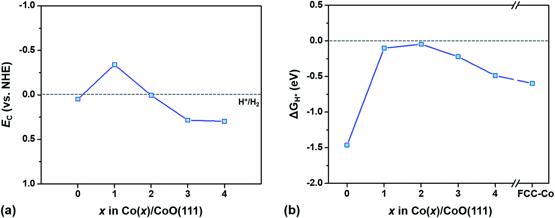 | ||
| Fig. 6 (a) Conduction band edge (EC) positions relative to the water reduction potential level (H+/H2) of CoO(111) layers in Co(x)/CoO(111) hybrid structures at pH = 1. (b) Free energy change for hydrogen adsorption (ΔGH*) on Co(x)/CoO(111) hybrid structures as a function of the number of Co layers (x) in the structure in pH = 1. All calculations are done with 1/4 H coverage. ΔGH* is also computed for pure FCC-Co(111) of 10 layers and shown in figure (b) with ‘FCC-Co’. | ||
The variation of the ECvs. H+/H2 with respect to the Co layer thickness is relevant to the charge state of the Co/CoO(111) surface. The Co(1)/CoO(111) structure contains many electrons in CoO layers during the process of electrochemical equilibration of Co and CoO layers as explained in Section 3.3 (Fig. 4) and in Fig. S10 in the ESI.† Therefore, when the Co(1)/CoO(111) structure is positioned in an aqueous environment, fewer electrons transfer from water to the CoO layer, which results in a more negative ECvs. H+/H2.13 However, in the Co(4)/CoO(111) hybrid structure, electrons move to the Co layer from the CoO layer during the process of electrochemical equilibration of the two materials (Fig. 4), and the CoO layer becomes comparatively positively charged. Therefore, the CoO layer in the Co(4)/CoO(111) structure accepts more electrons from water at the moment of immersion in water, exhibiting a more positive ECvs. H+/H2.13 According to our previous characterization in ref. 13, as the CoO surface is negatively charged, the EC is located at a higher energy level, i.e., a more negative potential level compared to the H+/H2 level. As the Co decoration layer becomes thicker in the Co/CoO(111) hybrid system, the EC varies from negative to more positive values (vs. NHE). This means that the CoO(111) layer is the most negatively charged in the Co(1)/CoO(111) structure, while it is more positively charged as the Co layer becomes thicker, which is in agreement with the interpretation in the section ‘SBH and band bending’.
However, we still do not know whether the photocatalytic HER occurs on the Co(1)/CoO(111) hybrid structure, only with the band edge positions of light absorbers (CoO in this study). This is because whether the energy of the photogenerated electrons is high enough to overcome the intrinsic barriers for the HER on the Co/CoO hybrid structure is unknown, without understanding the transition state of the HER on the Co/CoO structure.13 Therefore, we calculate the HER overpotential (ηHER) which indirectly implies the energy state of the transition state of the HER, that is, the energy barrier. The ηHER of a surface has been widely estimated by calculating free energy change for hydrogen adsorption, ΔGH* (|ΔGH*| = ηHER).37,38 A surface strongly binding with hydrogen has a more negative value, while stabilizing hydrogen adsorption on a surface with a more positive value is difficult. In particular, as the energy change of a surface approaches 0 (|ΔGH*| is smaller), ηHER of the surface becomes lower, resulting in a higher HER activity on the surface.75
Fig. 6(b) exhibits ΔGH* of Co(x)/CoO(111) hybrid structures as a function of x, showing how the HER activity varies with the thickness of the Co layers. All of the Co/CoO(111) structures have negative ΔGH* values, which means that bare CoO(111) and the Co/CoO hybrid structures strongly bind with hydrogen. The thin Co decoration on the CoO(111) layer including Co(1)/CoO(111) and Co(2)/CoO(111) considerably reduces ηHER by decreasing the binding strength with hydrogen. However, thicker Co layers increase ηHER, converging the ΔGH* value to that of the pure FCC-Co(111) slab. This parabolic variation of the ηHER with respect to the thickness of the Co layer is in good agreement with the experimental observation.24 The relative ηHER values of the pure Co, Co/CoO and pure CoO are in the order ηHERCo/CoO < ηHERCo < ηHERCoO as observed in a previous experiment.24
The very low ηHER values observed in the Co(1)/CoO(111) and/or Co(2)/CoO(111) structures (Fig. 6(b)) are also consistent with the experimentally measured HER overpotential, comparable to those of the commercial Pt/C catalyst.24,76 This low ηHER is possible because hydrogen adsorption–desorption readily occurs on the thin Co decorated hybrid structure, with almost ignorable electron exchange between the adsorbed hydrogen and the Co/CoO surface (Fig. S12 in the ESI†). Due to the negligible electron exchange, hydrogen binds on the Co/CoO surface strongly enough to stabilize the adsorption and weakly enough to be easily desorbed from the surface, which directly causes the most efficient HER (requiring less energy to generate H2). The high HER activity of Co(1)/CoO(111) is also confirmed from our ab initio MD study: Co(1)/CoO(111) in contact with liquid water at 298 K spontaneously dissociates water molecules to H* and OH*, and then creates H2 (Fig. S13 in the ESI†), while pure RS-CoO(111) and FCC-Co(111) are unable to form H2 (Fig. S14 in the ESI†). The different behaviors between the Co/CoO and CoO surfaces in an aqueous environment seem to originate from the very different ΔGH* (Fig. 6(b)): well-balanced adsorption–desorption of H on the Co/CoO(111) surface, while too strong binding of H on the CoO(111).
Both theoretical HER overpotentials estimated from the ECvs. H+/H2 (Fig. 6(a)) and the electrochemical HER overpotential estimated from the ΔGH* (Fig. 6(b)) predict that the most active structure for the HER is either the Co(1)/CoO(111) or Co(2)/CoO(111) structure. In order to determine which surface structure is indeed able to catalyze the HER under illumination without external bias, we use a criterion determining the feasibility of the photocatalytic HER as explained in ref. 14: the HER occurs when the EC is more negative than ηHER (=|ΔGH*|), according to ηHER(U) = ηHER(U = 0 V) + U, where the U value is determined by EC for photogenerated electrons. This criterion is based on the idea that only when the photogenerated electrons have enough energy to overcome the intrinsic barrier for the HER can HER occur under illumination without external bias. The predicted HER feasibility and the EC and ηHER values used for the determination are summarized in Table 1. According to the criterion, only Co(1)/CoO(111) can dissociate water by light absorption, and spontaneously create H2. However, the pure CoO(111) and hybrid structures with thicker Co layer decoration (beyond the 1 atomic Co layer) are unable to create hydrogen because the electrons photogenerated on them need more energy to overcome the intrinsic barrier for the HER.
| Number of Co layers, x, in Co(x)/CoO(111) | E C | η HER | f(HER) |
|---|---|---|---|
| 0 (pure CoO) | 0.048 | 1.465 | X |
| 1 | −0.340 | 0.103 | O |
| 2 | 0.006 | 0.047 | X |
| 3 | 0.284 | 0.222 | X |
| 4 | 0.296 | 0.487 | X |
SPR effect in Co layers
In addition to the light absorption by the semiconducting CoO layer, the SPR effect is expected in the Co layer when the Co/CoO(111) hybrid structures are exposed to light. The presence of a surface in metals can make ‘plasmons’ which are collective oscillations of free electrons.77,78 The surface plasmons cause the displacement of the electron gas with respect to their equilibrium position around positively charged ions. The localized surface plasmons (LSPs) in metal nanoparticles can be excited by irradiation at a specific frequency,77,79 resulting in the generation of hot carriers. Under the assumption that the Co layers (∼nm thick) decorated on the CoO(111) layer have the surface plasmon resonance frequency of the visible light spectrum (similar to that of the 20% stretched thin Co(111) slabs along the in-plane direction), we focus on the energy-population distribution of hot electrons in the Co layers in this study.The energy-population distribution of hot carriers resulting from the decay of the surface plasmons is the most critical factor that determines how many hot carriers can overcome the SBH at the metal/semiconductor interface and induce the HER/OER in the system.80–82 For the prediction of the distribution, we use eqn (3). The details are explained in Methods. Fig. 7 shows the predicted hot electron energy distribution in the Co layers in the Co/CoO hybrid structures under photon energies of 2 eV (Eph < ECoOg in Fig. 7(a)) and 2.6 eV (Eph ≥ ECoOg in Fig. 7(b)). The reason for the selection of Eph = 2 and 2.6 eV is to understand both when the CoO layer can absorb the incident visible light and not. Each Co layer has a slightly different energy-population distribution aspect because of the different LDOS of the Co layers on the CoO core. Owing to the higher photon energy, more hot electrons are populated under Eph = 2.6 eV than under Eph = 2 eV. Among the four hybrid structures, Co(4)/CoO(111) shows the highest hot electron population under both incident photon energies. This makes sense because more energy states are present around the EF for electron excitation (Fig. 5(a)), especially in the Co layers close to the interface (Co-0 and Co-1). Accordingly, more plasmons can be excited from the occupied states to the unoccupied states, and create a high population of hot electrons.
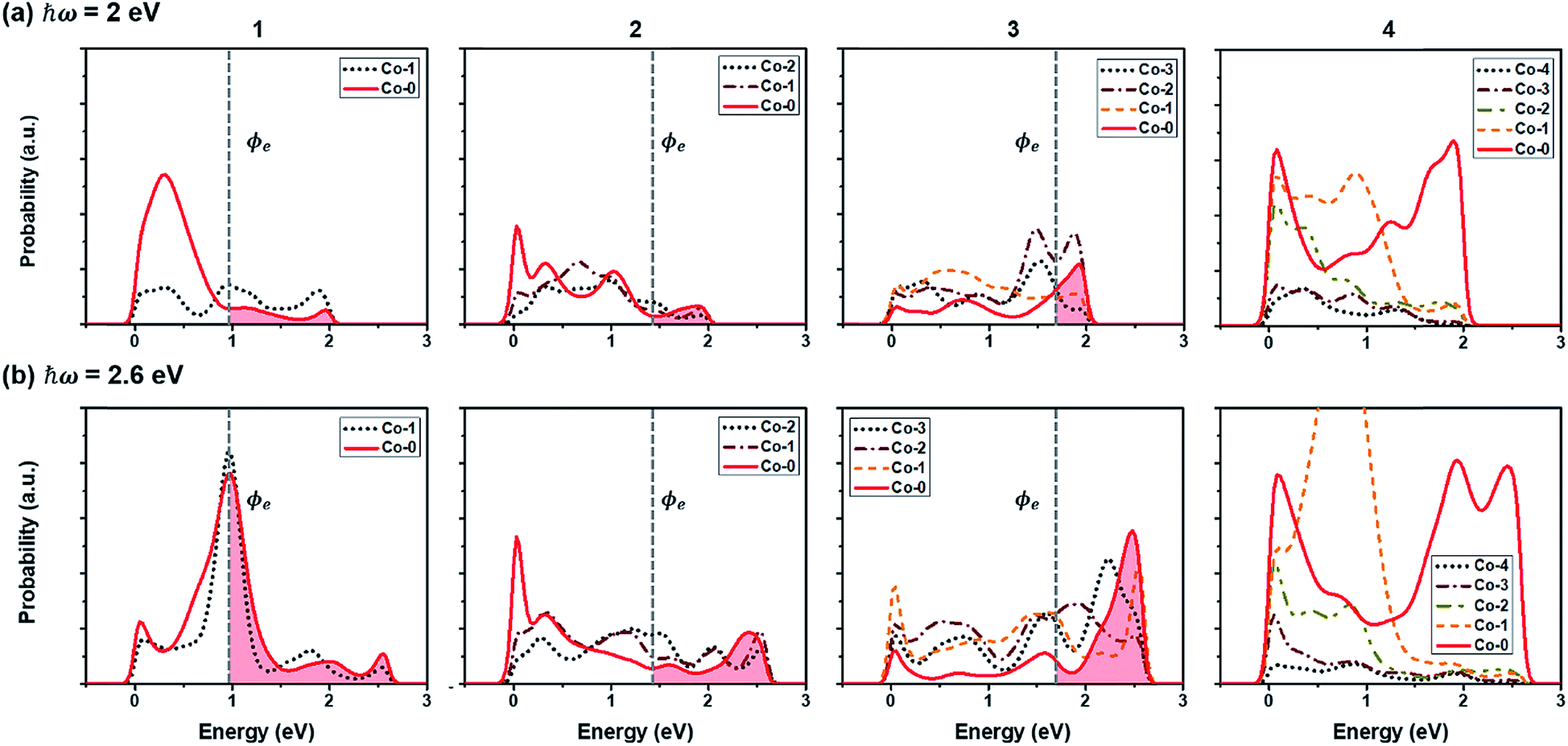 | ||
| Fig. 7 Energy-probability of hot electrons in each Co layer in Co(x)/CoO(111) under an incident photon energy of (a) 2 eV and (b) 2.6 eV. Numbers at the top of the graph denote the number of Co layers in the Co(x)/CoO(111) structures. The black dotted lines are the surface Co layer and the red solid lines are the interfacial Co layer among the Co layers. ϕe (vertical gray dotted line) is the SBH for electrons in each hybrid structure. Hot electrons overcoming the SBH from the interfacial Co layer (Co-0) to the CoO layers are shown in red color for example. | ||
To quantify how many hot electrons generated in the Co layer can overcome the SBH (E ≥ SBH) and go over to the adjacent CoO layer, we integrate the area of E ≥ SBH in Fig. 7(a) and (b) and the results are plotted in Fig. 8(a-1) and (b-1). Except for Co(4)/CoO(111) in which hot electrons cannot move to the CoO layer due to the SBH being higher than the energy which hot electrons have, the numbers of hot electrons overcoming their SBHs are similar in the three Co/CoO(111) structures with 1–3 Co layers. Under a higher photon energy (2.6 eV in Fig. 8(b-1)), more hot electrons can transfer to the CoO layer over the SBH than when under a lower photon energy (2 eV), since more hot electrons of high energy are populated under the higher photon energy.
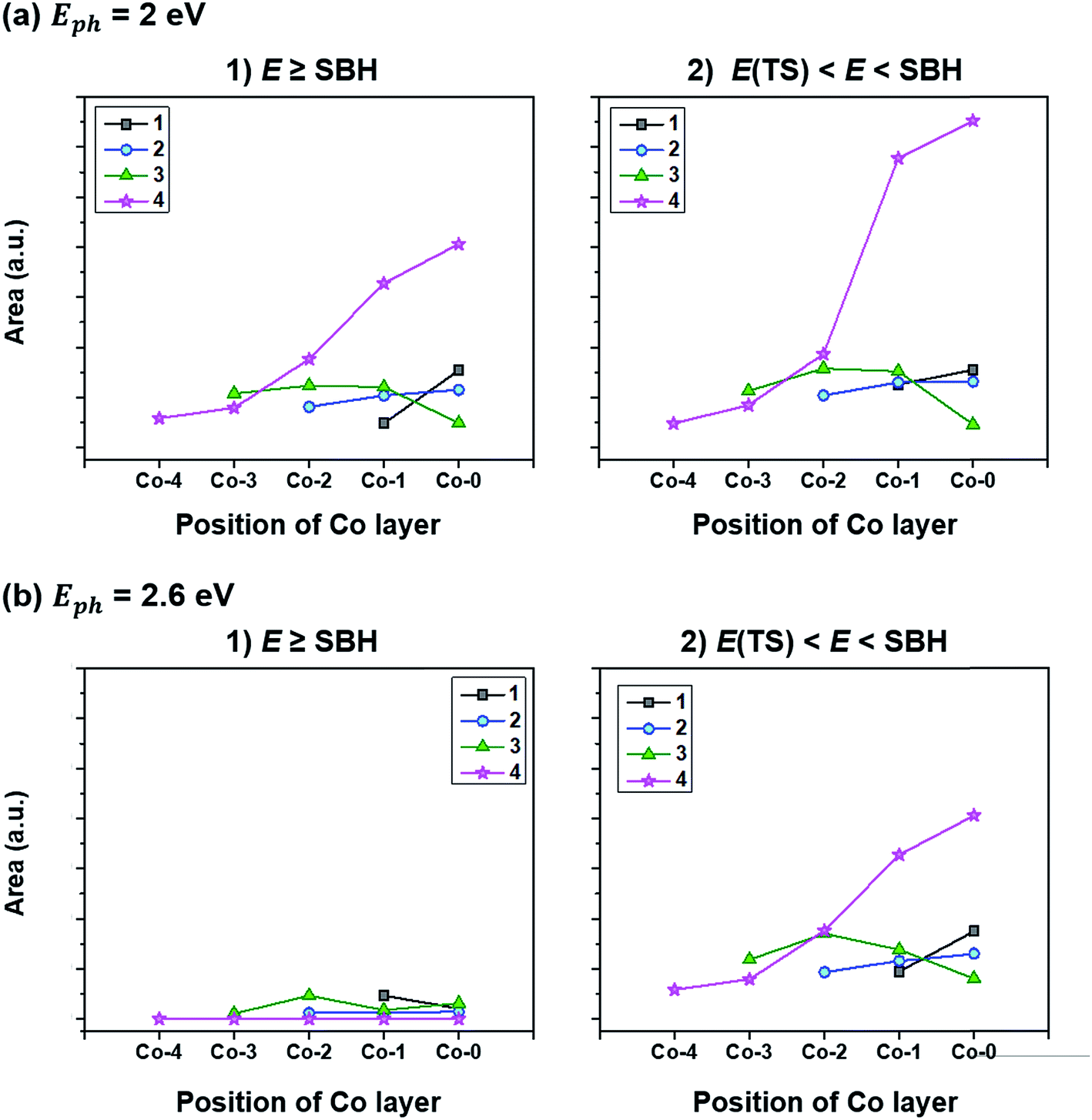 | ||
| Fig. 8 Population of hot electrons (denoted as ‘Area’ in the vertical axis) (1) overcoming the SBH for electrons with E ≥ SBH, (2) staying in the Co layers not going over to the adjacent CoO layers with E(TS) < E < SBH under an illumination of (a) Eph = 2 eV and (b) Eph = 2.6 eV. The number in the legend denotes the number of Co layers (x) in the Co(x)/CoO(111) hybrid structures. E is the energy of hot electrons and E(TS) is the energy required for triggering the HER, which is determined by the calculated HER overpotential, ΔGH*. All hot electrons generated in the Co layers of the Co/CoO(111) structures have higher energy (E) than the energy of the transition state of the HER (Fig. S15 in the ESI†); thus, the hot electrons generated in the Co layers can trigger the HER without further application of external energy. | ||
However, since hydrogen is much easier to be evolved on the Co(111) surface rather than on the CoO(111) surface, with a reduced HER overpotential (Fig. S11 in the ESI†), hot electrons staying in the Co layer (not overcoming the SBH) are more helpful for hydrogen evolution with the SPR effect. Therefore, we investigate the hot electron population staying in the Co layers in the Co/CoO(111) hybrid structure by integrating the area of the hot electron energy distribution below the SBH (E < SBH) under photon energies of 2 and 2.6 eV. The results are shown in Fig. 8(a-2) and (b-2). The population of hot electrons staying in the Co layer shows no big difference among the Co/CoO(111) structures with 1–3 Co layers, but a slight increase at a higher photon energy. Since some hot electrons (holes) overcome the SBH and some are left in the Co layers, hot electrons and holes existing in the confined space (like Co/CoO nanoparticles) are likely to recombine, resulting in the reduced efficiency of the SPR effect.
On the other hand, the Co layers in the Co(4)/CoO(111) structure have enormous hot electrons, especially in the Co-0 and Co-1 layers. These hot electrons in the thick Co layer face a very high SBH (ϕe); therefore, all the hot electrons stay in the Co layers. Furthermore, hot holes have a negative SBH (ϕh), and all hot holes transfer to the CoO layer without any barrier. Since HER energetically prefers to occur on the Co(111) surface (Fig. S11 in the ESI†), and the OER prefers to happen on the half hydroxylated CoO(111) surface,14 the efficient separation of hot electrons and holes minimizes their recombination rate, and accordingly, maximizes the photocatalytic efficiency for the HER/OER with the SPR effect.
Conclusions
This study identifies the interfacial characteristics of the Co/CoO(111) core–shell structures formed in a reducing environment. The created Co(111) layers are subjected to 20% tensile strain along the in-plane direction, forming an epitaxial structure with the underlying CoO(111) core. The structural state of the Co layers is close to the structure under the tensile deformation with Poisson's ratio of Co. The interfaces formed in the Co/CoO hybrid structures with different Co layer thicknesses have different magnitudes of SBH for electron and hole transfer and band bending aspects: (1) the SBH for electrons (for holes) increases (decreases) as the Co layer thickness increases, and (2) the degree of downward band bending of the CoO layer at the interface decreases, and it suddenly becomes reverse (upward band bending) above the critical Co thickness. This variation is closely related to the change in the relative electron affinities of the Co and CoO layers according to the change of work functions of the Co and CoO layers in the hybrid structures. The Co layer thickness-dependent interfacial characteristics determined by the electron transfer across the interface, eventually, determine the comparative charge states of the Co layer and Co/CoO interface, making the Co layer (CoO layer) more negatively (positively) charged. The different charge states of the Co surface and Co/CoO interface also vary the photocatalytic behaviors of the Co(x)/CoO(111) hybrid structures, i.e., both SPR effect in the Co layer and light absorption by the CoO layer for the HER.The comparative photocatalytic properties of the Co/CoO(111) hybrid structures predicted in this study are summarized in Table 2. Under illumination of Eph < ECoOg, only the SPR effect in the Co layer is expected since the CoO layer cannot absorb light. The SPR effect is high in the thick Co layer decorated structure (Co(4)/CoO(111)); therefore, hydrogen is expected to actively evolve on the hybrid structure from water splitting. Under illumination of Eph ≥ ECoOg, the SPR effect is still high in the thick Co layer deposited structure for H2 evolution, but the effect is more pronounced than that under smaller Eph. Another effect, the HER by the light absorption by the CoO layer, practically occurs only in the thin Co layer decorated hybrid structure such as Co(1)/CoO(111), because light absorbed by the CoO layer has enough energy to induce the HER on the Co/CoO(111) surface. In short, for H2 evolution from water splitting by the SPR effect, a thick Co layer is needed to be deposited on the CoO(111) layer, yet a thin Co layer is required for the optimal band edge and low HER overpotential to induce the HER on the hybrid structures under irradiation.
| Co layer thickness, x, in Co(x)/CoO(111) | E ph < Eg | E ph ≥ Eg | ||
|---|---|---|---|---|
| SPR effect | Light absorption | SPR effect | Light absorption | |
| 0 | X | X | X | X |
| 1 | Low | X | Low | O |
| 2 | Low | X | Low | X |
| 3 | Low | X | Low | X |
| 4 | High | X | High | X |
Conflicts of interest
There are no conflicts to declare.Acknowledgements
This work was supported by the MRSEC Program of the National Science Foundation (award number DMR – 1419807) and the Skolkovo Institute of Science and Technology (Skoltech) through the “Center for Research, Education and Innovation for Electrochemical Energy Storage” (contract number 186-MRA) and the KIST project (2E29340). This research used resources of the National Energy Research Scientific Computing Center (NERSC), a DOE Office of Science User Facility supported by the Office of Science of the U.S. Department of Energy under contract no. DE-AC02-05CH11231, and the resources of the Texas Advanced Computing Center (TACC) at The University of Texas at Austin have contributed to the research results reported within this paper. URL: http://www.tacc.utexas.edu.References
- A. L. Goff, V. Artero, B. Jousselme, P. D. Tran, N. Guillet, R. Métayé, A. Fihri, S. Palacin and M. Fontecave, Science, 2009, 326, 1384–1387 CrossRef PubMed.
- Y. Hou, B. L. Abrams, P. C. K. Vesborg, M. E. Björketun, K. Herbst, L. Bech, A. M. Setti, C. D. Damsgaard, T. Pedersen, O. Hansen, J. Rossmeisl, S. Dahl, J. K. Nørskov and I. Chorkendorff, Nat. Mater., 2011, 10, 434–438 CrossRef CAS PubMed.
- M. W. Kanan and D. G. Nocera, Science, 2008, 321, 1072–1075 CrossRef CAS PubMed.
- Q. Yin, J. M. Tan, C. Besson, Y. V. Geletii, D. G. Musaev, A. E. Kuznetsov, Z. Luo, K. I. Hardcastle and C. L. Hill, Science, 2010, 328, 342–345 CrossRef CAS PubMed.
- M. Risch, V. Khare, I. Zaharieva, L. Gerencser, P. Chernev and H. Dau, J. Am. Chem. Soc., 2009, 131, 6936–6937 CrossRef CAS PubMed.
- H. Dau, C. Limberg, T. Reier, M. Risch, S. Roggan and P. Strasser, ChemCatChem, 2010, 2, 724–761 CrossRef CAS.
- F. Jiao and H. Frei, Energy Environ. Sci., 2010, 3, 1018–1027 RSC.
- D. Shevchenko, M. F. Anderlund, A. Thapper and S. Styring, Energy Environ. Sci., 2011, 4, 1284–1287 RSC.
- T.-L. Wee, B. D. Sherman, D. Gust, A. L. Moore, T. A. Moore, Y. Liu and J. C. Scaiano, J. Am. Chem. Soc., 2011, 133, 16742–16745 CrossRef CAS PubMed.
- N. H. Chou, P. N. Ross, A. T. Bell and T. Don Tilley, ChemSusChem, 2011, 11, 1566–1569 CrossRef PubMed.
- L. Liao, Q. Zhang, Z. Su, Z. Zhao, Y. Wang, Y. Li, X. Lu, D. Wei, G. Feng, Q. Yu, X. Cai, J. Zhao, Z. Ren, H. Fang, F. Robles-Hernandez, S. Baldelli and J. Bao, Nat. Nanotechnol., 2014, 9, 69–73 CrossRef CAS PubMed.
- J. Ran, J. Ran, J. Zhang, J. Yu, M. Jaroniec and S. Z. Qiao, Chem. Soc. Rev., 2014, 43, 7787–7812 RSC.
- K. W. Park and A. M. Kolpak, J. Catal., 2018, 365, 115–124 CrossRef CAS.
- K. W. Park and A. M. Kolpak, J. Mater. Chem. A, 2019, 7, 6708–6719 RSC.
- X. Zhang, Z. Zhang, J. Liang, Y. Zhou, Y. Tong, Y. Wang and X. Wang, J. Mater. Chem. A, 2017, 5, 9702–9708 RSC.
- M. Hara, T. Kondo, M. Komoda, S. Ikeda, K. Shinohara, A. Tanaka, J. N. Kondo and K. Domen, Chem. Commun., 1998, 357–358 RSC.
- K. Sayama and H. Arakawa, J. Phys. Chem., 1993, 97, 531–533 CrossRef CAS.
- H. Kato and A. Kudo, Chem. Phys. Lett., 1998, 295, 487–492 CrossRef CAS.
- S. Yan, L. Wan, Z. Li and Z. Zou, Chem. Commun., 2011, 47, 5632–5634 RSC.
- B. Ma, F. Wen, H. Jiang, J. Yang, P. Ying and C. Li, Catal. Lett., 2010, 134, 78–86 CrossRef CAS.
- T. F. Yeh, C. Y. Teng, S. J. Chen and H. Teng, Adv. Mater., 2014, 26, 3297–3303 CrossRef CAS PubMed.
- S. Sun, W. Wang, D. Li, L. Zhang and D. Jiang, ACS Catal., 2014, 4, 3498–3503 CrossRef CAS.
- W. Fang, J. Liu, D. Yang, Z. Wei, Z. Jiang and W. Shangguan, ACS Sustainable Chem. Eng., 2017, 5, 6578–6584 CrossRef CAS.
- X. Liu, C. Dong, W. Dong, X. Wang, X. Yuan and F. Huang, RSC Adv., 2016, 6, 38515–38520 RSC.
- Ž. Kaminskienė, I. Prosyčevas, J. Stonkutė and A. Guobienė, Acta Phys. Pol., A, 2013, 123, 111–114 CrossRef.
- S.-F. Hung, F.-X. Xiao, Y.-Y. Hsu, N.-T. Suen, H.-B. Yang, H. M. Chen and B. Liu, Adv. Energy Mater., 2016, 6, 1501339 CrossRef.
- W. Fan and M. K. H. Leung, Molecules, 2016, 21, 180 CrossRef PubMed.
- X. Zhang, Y. L. Chen, R.-S. Liu and D. P. Tsai, Rep. Prog. Phys., 2013, 76, 046401 CrossRef PubMed.
- W. L. Roth, Phys. Rev., 1958, 110, 1333–1341 CrossRef CAS.
- U. D. Wdowik and K. Parlinski, Phys. Rev. B, 2007, 75, 104306 CrossRef.
- D. Herrmann-Ronzaud, P. Burlet and J. Rossat-Mignod, J. Phys. C: Solid State Phys., 1978, 11, 2123–2137 CrossRef CAS.
- G. Kresse and J. Hafner, Phys. Rev. B, 1993, 47, 558–561 CrossRef CAS PubMed.
- G. Kresse and J. Hafner, Phys. Rev. B, 1994, 49, 14251–14269 CrossRef CAS PubMed.
- J. P. Perdew, K. Burke and M. Ernzerhof, Phys. Rev. Lett., 1996, 77, 3865–3868 CrossRef CAS PubMed.
- Y. Wu, M. K. Y. Chan and G. Ceder, Phys. Rev. B, 2011, 83, 235301 CrossRef.
- K. W. Park and A. M. Kolpak, Commun. Chem. Search PubMed , accepted.
- B. Hinnemann, P. G. Moses, J. Bonde, K. P. Jørgensen, J. H. Nielsen, S. Horch, I. Chorkendorff and J. K. Nørskov, J. Am. Chem. Soc., 2005, 127, 5308–5309 CrossRef CAS PubMed.
- J. Greeley, T. F. Jaramillo, J. Bonde, I. Chorkendorff and J. K. Nørskov, Nat. Mater., 2006, 5, 909–913 CrossRef CAS PubMed.
- J. Rossmeisl, Z.-W. Qu, H. Zhu, G.-J. Kroes and J. K. Nørskov, J. Electroanal. Chem., 2007, 607, 83–89 CrossRef CAS.
- T. Gong and J. N. Munday, Opt. Mater. Express, 2015, 5, 2501–2512 CrossRef CAS.
- K. Wang, J. G. M. Sanderink, T. Bolhuis, W. G. van der Wiel and M. P. de Jong, Sci. Rep., 2015, 5, 15498 CrossRef CAS PubMed.
- W. Qin, J. Hou and D. A. Bonnell, Nano Lett., 2015, 15, 211–217 CrossRef CAS PubMed.
- S. Karube, H. Idzuchi, K. Kondou, Y. Fukuma and Y. Otani, Appl. Phys. Lett., 2015, 107, 122406 CrossRef.
- E. J. Monkman, C. Adamo, J. A. Mundy, D. E. Shai, J. W. Harter, D. Shen, B. Burganov, D. A. Muller, D. G. Schlom and K. M. Shen, Nat. Mater., 2012, 11, 855–859 CrossRef CAS PubMed.
- K. Mudiyanselage, S. D. Senanayake, L. Feria, S. Kundu, A. E. Baber, J. Graciani, A. B. Vidal, S. Agnoli, J. Evans, R. Chang, S. Axnanda, Z. Liu, J. F. Sanz, P. Liu, J. A. Rodriguez and D. J. Stacchiola, Angew. Chem., Int. Ed., 2013, 52, 5101–5105 CrossRef CAS PubMed.
- N. Floquet and L.-C. Dufour, Surf. Sci., 1983, 126, 543–549 CrossRef CAS.
- J. A. Little, J. W. Evans and K. H. Westmacott, Metall. Trans. B, 1980, 11B, 519–524 CrossRef CAS.
- A. K. Suszka, O. Idigoras, E. Nikulina, A. Chuvilin and A. Berger, Phys. Rev. Lett., 2012, 109, 177205 CrossRef CAS PubMed.
- S. E. Inderhees, J. A. Borchers, K. S. Green, M. S. Kim, K. Sun, G. L. Strycker and M. C. Aronson, Phys. Rev. Lett., 2008, 101, 117202 CrossRef CAS PubMed.
- S. Kim, H. Yoon, H. Lee, S. Lee, Y. Jo, S. Lee, J. Choo and B. Kim, J. Mater. Chem. C, 2015, 3, 100–106 RSC.
- L. Zou, J. Li, D. Zakharov, E. A. Stach and G. Zhou, Nat. Commun., 2017, 8, 307 CrossRef PubMed.
- R. L. Antón, J. A. González, J. P. Andrés, P. S. Normile, J. Canales-Vázquez, P. Muñiz, J. M. Riveiro and J. A. De Toro, Nanomaterials, 2017, 7, 61 CrossRef PubMed.
- S. Lee, J. Im, Y. Yoo, E. Bitzek, D. Kiener, G. Richter, B. Kim and S. H. Oh, Nat. Commun., 2014, 5, 3033 CrossRef PubMed.
- L. Tian, Y.-Q. Cheng, Z.-W. Shan, J. Li, C.-C. Wang, X.-D. Han, J. Sun and E. Ma, Nat. Commun., 2012, 3, 609 CrossRef PubMed.
- AZO materials, https://www.azom.com/article.aspx?ArticleID=596.
- C. N. Ávila-Neto, J. W. C. Liberatori, A. M. da Silva, D. Zanchet, C. E. Hori, F. B. Noronha and J. M. C. Bueno, J. Catal., 2012, 287, 124–137 CrossRef.
- C. Ge, X. Wan, E. Pellegrin, Z. Hu, S. Manuel Valvidares, A. Barla, W. I. Liang, Y. H. Chu, W. Zou and Y. Du, Nanoscale, 2013, 5, 10236–10241 RSC.
- M. Gierlings, M. J. Prandolini, H. Fritzsche, M. Gruyters and D. Riegel, Phys. Rev. B, 2002, 65, 0924071 CrossRef.
- M. R. Ghadimi, B. Beschoten and G. Güntherodt, Appl. Phys. Lett., 2005, 87, 261903 CrossRef.
- M. Kovylina, M. G. del Muro, Z. Konstantinović, M. Varela, O. Iglesias, A. Labarta and X. Batlle, Nanotechnology, 2009, 20, 175702 CrossRef PubMed.
- A. N. Dobrynin, D. N. Ievlev, K. Temst, P. Lievens, J. Margueritat, J. Gonzalo, C. N. Afonso, S. Q. Zhou, A. Vantomme and E. Piscopiello, Appl. Phys. Lett., 2005, 87, 012501 CrossRef.
- A. N. Dobrynin, K. Temst, P. Lievens, J. Margueritat, J. Gonzalo, C. N. Afonso, E. Piscopiello and G. Van Tendeloo, J. Appl. Phys., 2007, 101, 113913 CrossRef.
- M. Feygenson, Y. Yiu, A. Kou, K.-S. Kim and M. C. Aronson, Phys. Rev. B, 2010, 81, 195445 CrossRef.
- M. S. Batista, R. K. S. Santos, E. M. Assaf, J. M. Assaf and E. A. Ticianelli, J. Power Sources, 2003, 124, 99–103 CrossRef CAS.
- A. M. Karim, Y. Su, M. H. Engelhard, D. L. King and Y. Wang, ACS Catal., 2011, 1, 279–286 CrossRef CAS.
- A. R. Passos, L. Martins, S. H. Pulcinelli, C. V. Santilli and V. Briois, Catal. Today, 2014, 229, 88–94 CrossRef CAS.
- A. Kahn, Mater. Horiz., 2016, 3, 7–10 RSC.
- L. F. Zagonel, M. Bäurer, A. Bailly, O. Renault, M. Hoffmann, S.-J. Shih, D. Cockayne and N. Barrett, J. Phys.: Condens. Matter, 2009, 21, 314013 CrossRef CAS PubMed.
- T. Okazawa, M. Fujiwara, T. Nishimura, T. Akita, M. Kohyama and Y. Kido, Surf. Sci., 2006, 600, 1331–1338 CrossRef CAS.
- H.-X. Deng, J. Li, S.-S. Li, J.-B. Xia, A. Walsh and S.-H. Wei, Appl. Phys. Lett., 2010, 96, 162508 CrossRef.
- M. J. Redman and E. G. Steward, Nature, 1962, 193, 867 CrossRef CAS.
- D. C. Kahn and R. A. Erickson, Phys. Rev. B, 1970, 1, 2243–2249 CrossRef.
- B. A. Pinaud, Z. B. Chen, D. N. Abram and T. F. Jaramillo, J. Phys. Chem. C, 2011, 115, 11830–11838 CrossRef CAS.
- Y. J. Matsumoto, Solid State Chem., 1996, 126, 227–234 CrossRef CAS.
- J. K. Nørskov, T. Bligaard, A. Logadottir, J. R. Kitchin, J. G. Chen, S. Pandelov and U. Stimming, J. Electrochem. Soc., 2005, 152, J23–J26 CrossRef.
- X. Liu, X. Wang, X. Yuan, W. Dong and F. Huang, J. Mater. Chem. A, 2016, 4, 167–172 RSC.
- S. A. Maier, Plasmonics: Fundamentals and Applications, Springer, 2007 Search PubMed.
- C. Kittel and P. McEuen, Introduction to Solid State Physics, New York, Wiley, 1996 Search PubMed.
- U. Kreibig and M. Vollmer, Optical Properties of Metal Clusters, Berlin, Springer, 1995 Search PubMed.
- R. Sundararaman, P. Narang, A. S. Jermyn, W. A. Goddard III and H. A. Atwater, Nat. Commun., 2014, 5, 5788 CrossRef CAS PubMed.
- S. Shuang, R. Lv, Z. Xie and Z. Zhang, Sci. Rep., 2016, 6, 26670 CrossRef CAS PubMed.
- H. Wang, H. Wang, T. You, W. Shi, J. Li and L. Guo, J. Phys. Chem. C, 2012, 116, 6490–6494 CrossRef CAS.
Footnote |
| † Electronic supplementary information (ESI) available. See DOI: 10.1039/c9ta04508b |
| This journal is © The Royal Society of Chemistry 2019 |