
 Open Access Article
 This Open Access Article is licensed under a
 Creative Commons Attribution 3.0 Unported Licence
Highly efficient and stable inverted perovskite solar cells using down-shifting quantum dots as a light management layer and moisture-assisted film growth†
Mohammad Mahdi
Tavakoli
 *ab,
Hadi Tavakoli
Dastjerdi
c,
Daniel
Prochowicz
d,
Pankaj
Yadav
e,
Rouhollah
Tavakoli
a,
Michael
Saliba
f and
Zhiyong
Fan
*gh
*ab,
Hadi Tavakoli
Dastjerdi
c,
Daniel
Prochowicz
d,
Pankaj
Yadav
e,
Rouhollah
Tavakoli
a,
Michael
Saliba
f and
Zhiyong
Fan
*gh
aDepartment of Materials Science and Engineering, Sharif University of Technology, 14588 Tehran, Iran
bDepartment of Electrical Engineering and Computer Science, Massachusetts Institute of Technology, Cambridge, MA 02139, USA. E-mail: mtavakol@mit.edu
cDepartment of Materials Science and Engineering, Massachusetts Institute of Technology, Cambridge, MA 02139, USA
dInstitute of Physical Chemistry, Polish Academy of Sciences, Kasprzaka 44/52, 01-224 Warsaw, Poland
eDepartment of Solar Energy, School of Technology, Pandit Deendayal Petroleum University, Gandhinagar-382 007, Gujarat, India
fAdolphe Merkle Institute, Chemins des Verdiers 4, CH-1700 Fribourg, Switzerland
gDepartment of Electronic and Computer Engineering, The Hong Kong University of Science and Technology, Clear Water Bay, Kowloon, Hong Kong SAR, China. E-mail: eezfan@ust.hk
hHKUST-Shenzhen Research Institute, No. 9 Yuexing First RD, South Area, Hi-tech Park, Nanshan, Shenzhen 518057, China
First published on 20th May 2019
Abstract
Stability is one of the key challenges for perovskite solar cells (PSCs) to become an industrial reality. In this work, we present two novel strategies to significantly improve the stability of PSCs using environmental humidity and down-shifting quantum dots (QDs). We first improve the crystallinity of double-cation Cs/FA perovskite by annealing films in 40% relative humidity (RH). Our results reveal that the grain size, carrier lifetime and crystallinity of perovskite films are enhanced drastically due to the humidity. Next, we apply a thin layer of CdSe/CdS quantum dots (QDs) on the back of the device to convert high energy UV light into lower energy visible wavelengths. Using this modification, we improve not only the UV stability but also the device performance of the PSCs. Based on these modifications, we achieve an inverted PSC with a maximum power conversion efficiency (PCE) of 20.7%. Moreover, our modified device shows a great operational stability under continuous illumination after 300 h with only 15% PCE loss. We also examine the UV stability of our devices and find that the modified PSC retains 79% of its initial PCE after 150 h under continuous illumination outperforming the reference device.
Introduction
Organometallic halide perovskites have an ABX3 structure, where A is cesium (Cs), methylammonium (MA) or formamidinium (FA), B is Pb or Sn, and X is Cl, Br or I.1–3 These compounds emerge as attractive light harvesting materials due to their intriguing optoelectronic properties such as high mobility, long carrier life time, band gap tunability, great absorption and ease of fabrication. In the past few years, perovskite solar cells (PSCs) showed tremendous progress with a certified PCE that is over 24%.4–9 Besides the further improvement of photovoltaic performance, long-term device stability is a key challenge for the commercialization of PSCs.10,11 The main reported strategies to improve stability include compositional engineering,12–14 interface modification,15,16 passivation techniques,17,18 using water-repellent materials19–22 and device packaging via encapsulation methods.23,24 These techniques enhance the device performance and stability by reducing the recombination sites and improving the quality of PSCs.25–27 Among the above approaches, the positive effects of humidity either in perovskite precursors28 or during the annealing step29 on the improvement of perovskite crystallinity have been reported by many researchers in this field. In general, a perovskite compound decomposes in a highly humid environment; however, an optimum level of moisture can have a positive impact on the optical properties and the morphology of perovskite films.30 For example, Contreras-Bernal et al.31 studied the effect of the humidity level during the fabrication process on the stability of PSCs and found that the as-prepared perovskite films under controlled humid conditions below 50% RH show better stability in a humid environment.Another drawback of perovskite materials is the presence of organic components that can decompose upon exposure to high energy UV light.32–34 One promising strategy to tackle this issue is the application of a protective layer on the top of a PSC that blocks the UV photons from reaching the perovskite material and converts them into lower energy visible photons.35–37 In this context, luminescent down shifting materials such as fluorinated photopolymers,38 complex compounds such as lanthanide luminescence and europium complexes,35,39 and QDs40–43 demonstrate potential to improve the light absorption and current density and reduce the degradation of PSCs under UV light.
In this work, we demonstrate effective strategies to improve the stability and performance of inverted PSCs based on a Cs/FA double A-cation composition via annealing perovskite films in a humid environment and application of a luminescent down-shifting quantum dot (QD) layer. We find that the annealing of perovskite films in an ambient air atmosphere with 40% RH effectively increases the grain size and film quality leading to an improved carrier lifetime. Further deposition of a core–shell CdSe/CdS QD thin film on the back side of a PSC successfully suppresses the degradation of the perovskite material under irradiation of UV light. As a result, the inverted PSC yields in a high PCE of 20.70% and improved stability under the conditions of continuous UV illumination for 150 h. These results open new possibilities for the development of efficient and stable PSCs.
Results and discussion
Here, we use a double A-cation Cs/FA perovskite composition (see details in the ESI†) as an absorber layer embedded in an inverted architecture. The perovskite film was deposited using the anti-solvent method27 and annealed at 110 °C for 40 min in a nitrogen glovebox (the reference) and in a dry air box with 40% RH (the ambient air sample) for comparison. Fig. 1a and b show the schematics of the perovskite films deposited on ITO glass annealed inside the nitrogen glovebox and in ambient air, respectively. Top-view scanning electron microscopy (SEM) images of both samples reveal that the average grain size increases significantly from 320 to 760 nm by annealing the perovskite film under ambient air conditions (Fig. 1c and d). This indicates that moisture has a positive effect on the improvement of the grain size and crystallinity of perovskite films, resulting in a reduction of the formed grain boundaries.44,45 This result is also confirmed by atomic force microscopy (AFM), as shown in Fig. 1e and f. Moreover, the surface roughness of the perovskite films is reduced from 31 ± 8 nm to 25 ± 6 nm after annealing in ambient air as compared to the reference sample (see Fig. S1†).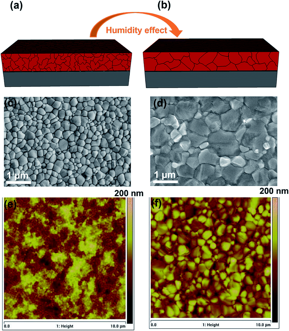 | ||
| Fig. 1 Schematic representations of the perovskite films after annealing at 110 °C (a) in a nitrogen and (b) humid atmosphere (∼40% RH). Top-view SEM and AFM images of the perovskite films annealed inside a nitrogen-filled glovebox (c and e) and in ambient air (d and f), respectively. | ||
The optical properties of the perovskite films are examined by UV-visible absorption and photoluminescence (PL) measurements. As shown in Fig. 2a, the optical absorption and emission of the perovskite film annealed in ambient air are stronger than those observed for the reference, indicating a significant effect of humidity on the perovskite crystallinity and grain size. Moreover, we find that the band edges of the absorption spectra slightly red shift when the film is annealed in ambient air. Similarly, the PL spectrum shows a correspondingly small red shift with respect to the reference film. The red shift in both UV-vis and PL spectra might be caused by the larger grain size, consistent with the SEM images.46–48 To further determine the carrier lifetimes of the resulting perovskite films, time-resolved PL (TRPL) measurements were performed. The enhancement of the carrier lifetime from 3.39 to 7.36 ns is observed for the perovskite film annealed in ambient air, which could be due to its larger grain size and better crystallinity (see Fig. 1). The fitting parameters of TRPL data are listed in Table S1.†Fig. 2c shows the X-ray diffraction (XRD) patterns of the perovskite films annealed in the different environments. Both films exhibit a similar structure with the perovskite peaks at ∼14.0° and ∼28.0° originating from the (110) and (220) planes of the perovskite phase45 and the intensity of these diffraction peaks is more than that for the film annealed in ambient air indicating its higher crystallinity. In addition, in both samples the characteristic diffraction peaks specific to PbI2 and non-perovskite yellow phase δ-FAPbI3 were not observed. These results demonstrate that the annealing of the perovskite films in ambient air facilitates its crystal growth.
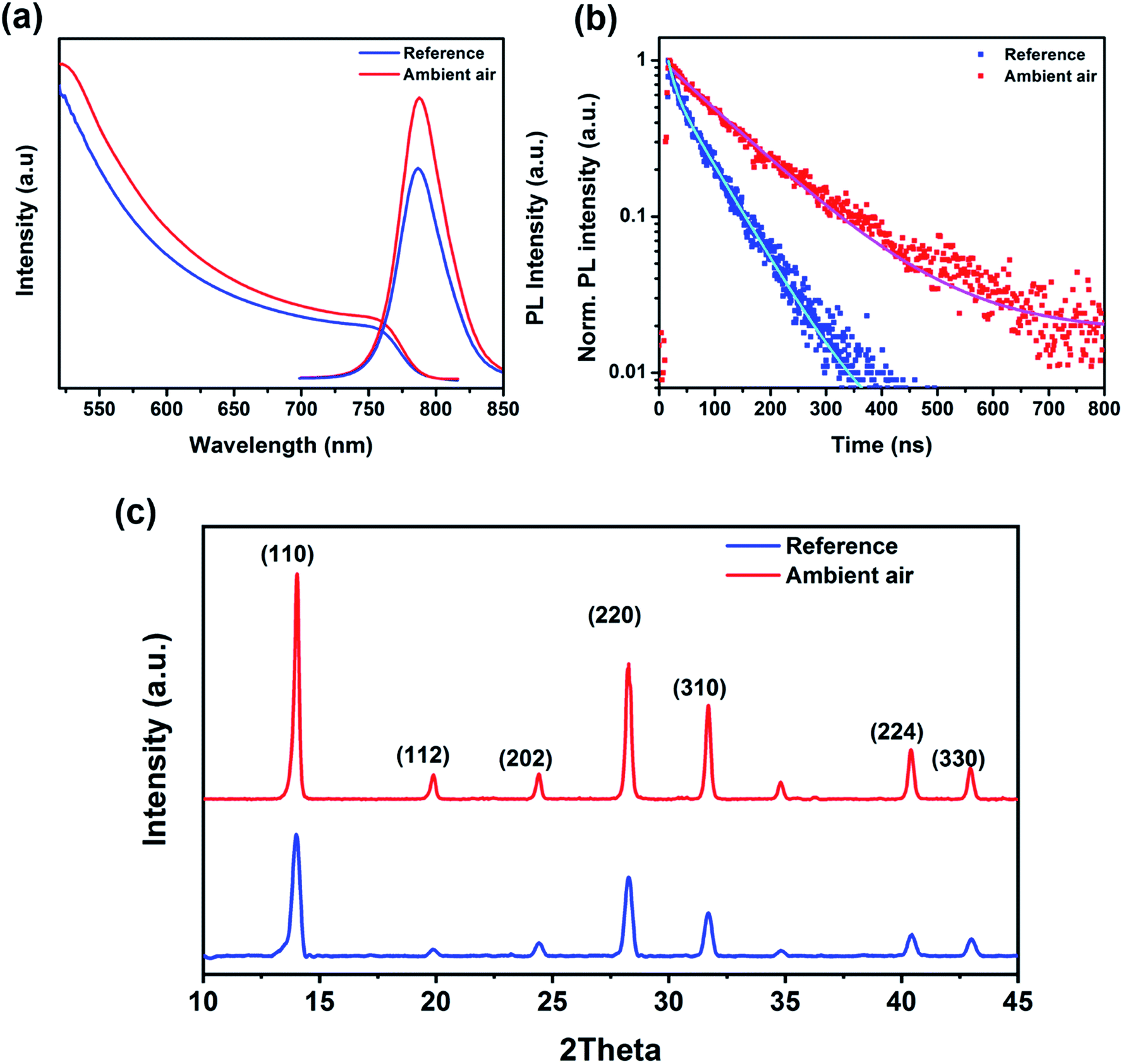 | ||
| Fig. 2 Characterization of the perovskite films annealed in a nitrogen glovebox and ambient air. (a) UV-visible and photoluminescence spectra, (b) time-resolved photoluminescence (TRPL) spectra and (c) XRD patterns. | ||
To study the impact of the humidity effect on the resulting photovoltaic properties, we fabricate devices with an inverted architecture of ITO/NiO/perovskite/C60/BCP/Ag. Fig. 3a shows the cross-sectional SEM image of an inverted PSC device based on the perovskite film fabricated in ambient air. The device is comprised of indium-doped tin oxide (ITO) as a transparent electrode, a 40 nm-thick nickel oxide (NiO) layer as a hole transporting layer (HTL), a 450 nm-thick perovskite film as an absorber layer, a 23 nm thick C60 layer as an electron transporting layer (ETL), an 8 nm-thick layer of bathocuproine (BCP) as a buffer layer, and a silver (Ag) electrode with a thickness of 100 nm. Fig. 3b shows the current density–voltage (J–V) curves of the best performing PSC devices based on perovskite films fabricated under nitrogen and ambient air conditions. The summary of photovoltaic (PV) parameters is given in Table 1. The reference device shows an open circuit voltage (Voc) of 1125 mV, a short circuit current density (Jsc) of 22.1 mA cm−2, a fill factor of 75.6% and a PCE of 18.8%. However, the ambient air device has a superior photovoltaic performance with a Voc of 1141 mV, a Jsc of 23.05 mA cm−2, a fill factor of 77%, and a high PCE of 20.2%. These results indicate that the humidity effect has a great impact on all PV parameters for the investigated PSC. By controlling the level of moisture during the annealing step, the quality of the perovskite film can be improved drastically as substantiated by the presented characterization technique. We also track the maximum power point (MPP) of the best-performing devices as shown in Fig. 3c. The devices based on perovskite films annealed in the nitrogen glovebox and ambient air show MPPs of 18.4% and 20.1% over 60 s, confirming their performance stability under light. The statistics of the collected PV parameters for the corresponding devices are shown in Fig. S2.† The average values of all PV parameters are improved drastically as compared to the reference cells. To further investigate the humidity effect on the Jsc of these devices, we measured their external quantum efficiency (EQE). The ambient air device exhibits a higher EQE (more than 85%) over the entire spectrum as compared to the reference cell, resulting in an integrated Jsc of 21.87 mA cm−2 higher than that of the reference device with 20.92 mA cm−2 (Fig. 3d). These results indicate a good consistency of the integrated Jsc with the Jsc values obtained from the J–V curves. The higher current density of the ambient air device can be ascribed to the lower recombination sites due to the better crystallinity and morphology of the perovskite.
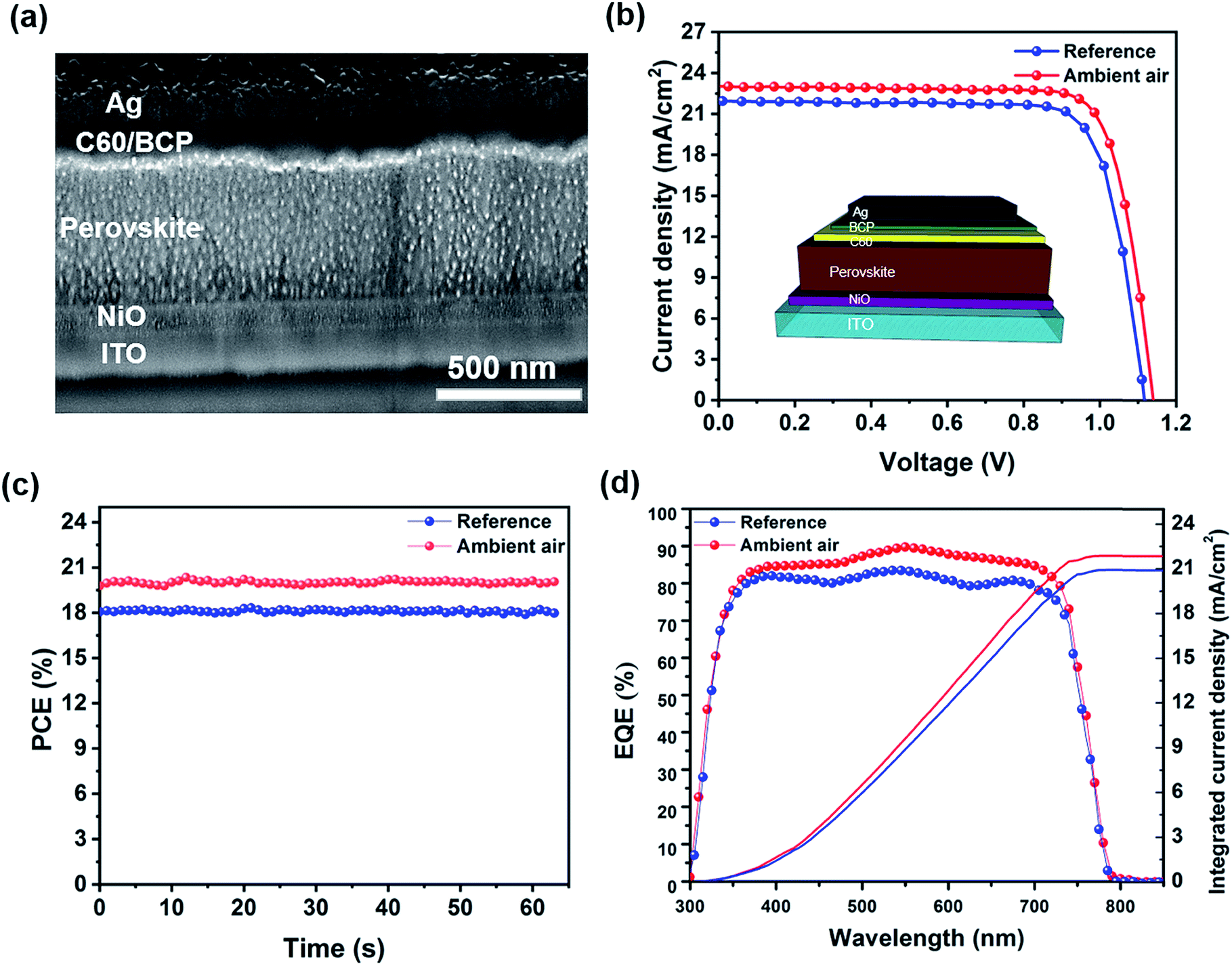 | ||
| Fig. 3 (a) Cross-sectional SEM image, (b) J–V curves, (c) maximum power point tracking and (d) EQE spectra of the PSC devices based on perovskite films annealed in the nitrogen glovebox and ambient air. | ||
| Device | V oc (mV) | J sc (mA cm−2) | FF (%) | PCE (%) | MPP (%) |
|---|---|---|---|---|---|
| Reference | 1125 | 22.10 | 75.6 | 18.8 | 18.4 |
| Ambient air | 1141 | 23.05 | 77 | 20.2 | 20.1 |
Fig. S3†shows the statistics of hysteresis indices (HIs) for the investigated devices. Our results show an average HI of 1.2% for the devices based on perovskite films annealed in ambient air, which is lower than that observed for reference devices (1.6%). This result shows the impact of perovskite crystallinity on the mitigation of hysteresis behavior in the investigated PSCs.
In order to study the effect of humidity on the PV parameters of the PSCs, electrochemical impedance spectroscopy (EIS) was employed. Fig. S4† illustrates the Nyquist plots of the reference device and modified PSC under dark conditions. The series resistance (Rs) and recombination resistance (RRec) of the corresponding PSCs were estimated by fitting the Nyquist plots using the equivalent circuit shown in the inset image of Fig. S4.† Our results indicate that the ambient air PSC has a lower Rs (18.6 Ω) as compared to the reference cell (25.2 Ω), which explains the higher FF of the modified PSC.9 Additionally, the RRec of the reference cell and modified PSC is 306 and 415 Ω cm−2, respectively. It is clear that the modified PSC has a larger recombination resistance, i.e., lower recombination than that of the reference device, resulting in a PSC with a higher Voc.30 This effect is originated from the quality of the perovskite film annealed in ambient air with a larger grain size than that of the reference sample (Fig. 1d and f). Consequently, the modified PSC has lower grain boundaries and recombination sites, which results in a higher Voc as well as PCE.9,30
Apart from the high efficiency, the stability of PSCs under illumination, heat, moisture and also UV light irradiation remains a key challenge for the commercialization of PSCs.3 To address the photostability issue, we deposited a thin layer of core–shell CdSe/CdS QDs (with 85% PL quantum yield (PLQY)) as a down-shifting layer on the back of the device and optimize its thickness by controlling the QD concentration in hexane from 0 to 2.0 wt%. Essentially, CdSe/CdS QDs possess a wide absorption band in the UV region and can convert high energy photons into low energy photons. This procedure should result in more efficient light absorption and higher device stability. Fig. 4a shows the emission of the QD layer with different dot concentrations. As seen, this layer shows a strong red emission, which is intensified by increasing the thickness of the QD layer. The steady-state PL spectrum of CdSe/CdS QDs shows a PL peak position at 620 nm (Fig. S5†). Fig. S6† shows that upon increasing the thickness of the QD layer (using more concentrated solutions), the PL intensity of the QD layer is increased, indicating a stronger down-shifting effect. The transmittance spectra of the QD layer with different thicknesses are shown in Fig. 4b. It is clear that the QD layer mostly blocks the light from 300 to 500 nm. In the next step, we try to find an optimum thickness of this layer, which will have a superior impact on the final device performance. The PV results for this optimization are listed in Table S2.† We find that a QD concentration of 1.0 wt% is the optimum value, increasing the current density as well as blocking the high energy photons. Fig. 4c depicts the J–V curves of the best PSC devices annealed in ambient air without and with the QD layer. Table 2 summarizes the collected PV parameters of the corresponding devices. By applying the QD layer on the back of the device, the Jsc is increased from 23.1 to 23.6 mA cm−2 with a slight enhancement in the Voc from 1141 to 1143 mV, resulting in a PCE of 20.7%, which is higher than that of the PSC device without the QD layer (20.08%). Moreover, the obtained high PCE is among the highest efficiencies reported for inverted PSCs.49Fig. 4d demonstrates the EQE curves of the corresponding devices without and with the QD layer. It is evident that the EQE of the QD based device is higher in the high energy photon range, i.e. the UV region, due to the down-shifting properties of the QD layer. In fact, the UV light in this sample is converted to the visible range (around 620 nm) and absorbed in the perovskite film, which results in higher EQE at shorter wavelengths. Consequently, the integrated Jsc calculated from the EQE curve of the PSC with the QD layer is estimated to be 22.3 mA cm−2, which is 0.6 mA cm−2 higher than that of the reference sample. These results are in agreement with the Jsc values obtained from the J–V curves. For the devices without the down-shifting QD layer, the high energy photons, with wavelengths of <∼400 nm, get significantly absorbed in the FTO electrode and NiOx HTL, before they can reach the perovskite layer. On the other hand, even for the small percentage of incident high energy photons that could reach the perovskite layer, their contribution to carrier generation would be very small due to high levels of thermalization in the perovskite layer. During the EQE measurement of the PSCs with the QD layer, the high energy photons that would otherwise contribute very little to carrier generation for the reference PSC are absorbed by the QD layer and get re-emitted at longer wavelengths. The re-emitted photons at longer wavelengths are highly absorbed by the perovskite layer and effectively contribute to carrier generation resulting in improved EQE in the UV range and slightly improved EQE in the visible region.
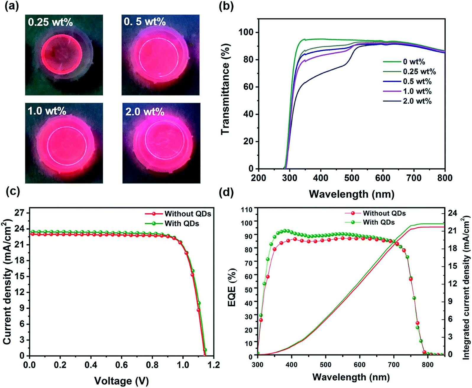 | ||
| Fig. 4 (a) Photographs of the emission of CdSe/CdS QDs deposited on glass with different thicknesses under UV light and (b) transmittance spectra of the corresponding QD films. (c) J–V curves and (d) EQE spectra of PSCs without and with a down-shifting QD layer. | ||
| Device | V oc (mV) | J sc (mA cm−2) | FF (%) | PCE (%) |
|---|---|---|---|---|
| Without QDs | 1141 | 23.1 | 76.2 | 20.08 |
| With QDs | 1143 | 23.6 | 76.8 | 20.70 |
Fig. 5a and b show the contact angle (CA) of a water droplet on pure glass and a QD layer deposited on glass under UV illumination, respectively. Interestingly, by applying the QD layer on the surface of glass, i.e., the back of the PSC device, the CA is increased from 31° to 94°. This result indicates that the QD layer can work as a protection layer for PSCs in a solar farm against moisture. To study the effect of down-shifting materials on the device stability, we perform stability tests under continuous illumination and UV light irradiation. Fig. 5c shows the stability results of the PSCs under continuous illumination for 300 h in a nitrogen environment. The PSC device annealed in ambient air with the QD layer shows the best stability with only 15% PCE loss after 300 h illumination. In turn, the analogous device without the QD layer has a 28% PCE loss, which is more stable than the reference PSC with a 44% PCE drop. These results highlight the effect of humidity on the perovskite crystallinity as well as the device stability. We further examine the stability of PSCs without and with QD layers under continuous UV light irradiation. As shown in Fig. 5d, the protected device retains 79% of its initial PCE after exposure to continuous UV light over 150 h, and is more stable than the reference device without QD layers (retaining only 48% of its initial PCE value). This enhancement stems from the QD down-shifting layer, which blocks the UV light and improves the device stability.
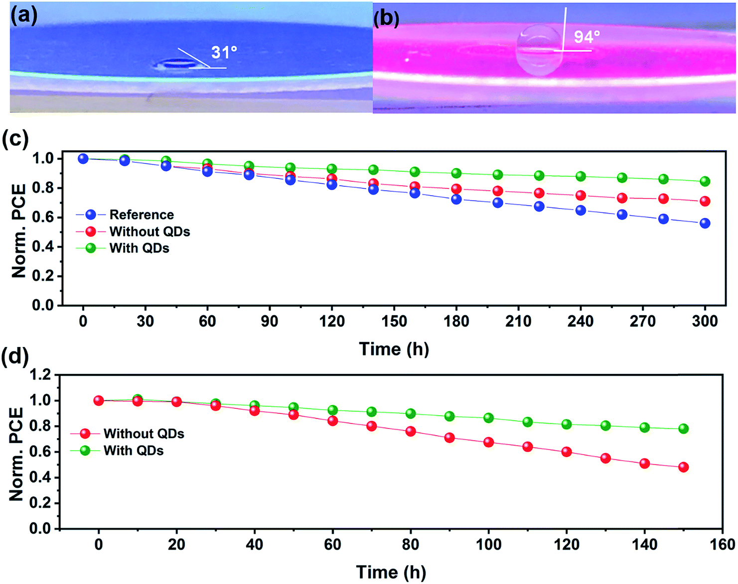 | ||
| Fig. 5 Contact angle measurement of (a) pure glass and (b) the down-shifting layer on glass using a water droplet. Stability test of the PSC devices (c) under continuous illumination for 300 h and (d) under UV light for 150 h. | ||
Conclusions
In summary, we develop two strategies to improve the device performance and stability of inverted PSCs based on a Cs/FA double A-cation composition, i.e. annealing in an ambient environment with 40% RH and applying a down-shifting layer on the back of the PSC. We demonstrate that ambient air annealing of perovskite films improves the grain size and crystallinity leading to a longer carrier lifetime as compared to perovskite films annealed in a nitrogen glovebox. Based on this strategy, we improve the device performance from 18.8% to 20.2% and enhance its operational stability. Additionally, we show that the application of a CdSe/CdS QD layer on the back of the PSC as a down-shifting layer results in a higher Jsc and PCE, with a maximum efficiency of 20.7% and better light stability. Moreover, the device with the QD layer maintains 79% of its initial PCE value after exposure to continuous UV illumination for 150 h, a clear improvement compared to the reference sample that loses 52% of its initial PCE.Experimental section
Device fabrication
ITO glass was patterned using zinc powder and diluted HCl solution and then cleaned in the following solutions for 20 min using ultrasonic treatment, respectively: Triton X100 (1% vol in deionized (DI) water), DI water, acetone, and ethanol. The surface of the cleaned ITO glass was treated using UV ozone before the deposition of NiO as an HTL. A precursor solution of NiO (1 M) was prepared by dissolving nickel(II) nitrate hexahydrate (Ni(NO3)2·6H2O, Sigma Aldrich) in ethylene glycol with added ethylenediamine (Sigma Aldrich) and lithium acetate. Then, this solution was spin-coated on the substrates at 3000 rpm for 100 s, followed by annealing at 300 °C in air for 1 h.After treating the surface of the NiO layer using UV ozone, a precursor solution of Cs/FA perovskite containing PbI2 (1.26M, TCI), FAI (1.08M, Dyesol), and CsCl (0.12M, TCI) in a mixed solvent of DMF and DMSO (4/1 vol%) was spin coated in two steps: 1000 rpm for 10 s and 6000 rpm for 20 s (ramp rate: 2000 rpm s−1). During spin-coating, 60 μL of chlorobenzene (CB) (on a 0.5 inch2 substrate) anti-solvent was added dropwise on the film, 10 s before the end of the spinning. 1-adamantylamine hydrochloride (ADAHCl) was dissolved in CB (3 mg mL−1) for the passivation purpose as reported previously. Afterward, the films were annealed at 110 °C for 40 min in either a nitrogen glovebox or ambient air with 40% RH. After annealing, the films were transferred to a thermal evaporator and C60 (23 nm), BCP (8 nm), and Ag (100 nm) were evaporated on the perovskite film, as an ETL, buffer layer, and electrode, respectively. For the deposition of the core–shell structure of CdSe/CdS QDs (Sigma Aldrich), solutions with different concentrations in hexane (0, 0.25, 0.5, 1.0, and 2.0 wt%) were prepared and deposited at 3000 rpm for 30 s to obtain layers with different thicknesses.
Film characterization
The morphology of the perovskite films was studied using scanning electron microscopy (SEM, ZEISS Merlin), X-ray diffraction (XRD, Bruker D8 X-ray Diffractometer (USA)), and atomic force microscopy (AFM, NanoScope IIIa/Dimension 3100). The optical properties of the films were analyzed by UV-visible (Varian Cary 5) and photoluminescence (PL, a Fluorolog 322 (Horiba Jobin Ybon Ltd)) measurements. The PL excitation was at λ = 460 nm. For lifetime measurement, a picosecond pulsed diode laser (EPL-405, with an excitation wavelength of λ = 405 nm and a pulse width of 49 ps) was employed and the data were fitted using an exponential equation (I(t) = ai exp(−t/τi)), where ai and τi are the amplitude and the lifetime of each term, respectively.Device measurement
All devices were measured by using a digital source meter (Keithley model 2400, USA) and a 450 W xenon lamp (Oriel, USA). The simulated light was filtered using a Schott K113 Tempax sunlight filter (Präzisions Glas & Optik GmbH, Germany). For J–V measurement, the voltage scan rate and the dwell time were set to 10 mV s−1 and 15 s, respectively. To simulate AM 1.5 G conditions, the light intensity was adjusted to 1000 W m−2. The hysteresis indices of PSCs were calculated using the following formula: hysteresis index = ((PCEbackward − PCEforward)/PCEbackward) × 100. The external quantum efficiency of the devices was recorded by using a commercial apparatus (Arkeo-Ariadne, Cicci Research s.r.l.) with a 300 Watts xenon lamp.The stability measurement (including UV stability) was performed in a nitrogen glovebox. The devices were kept under simulated standard AM 1.5 G conditions using an array of white LED lamps and the maximum power point (MPP) was measured over time. For UV stability, a UV lamp with 100 mW cm−2 was used. EIS measurement was performed using Autolab with a frequency range from 200 mHz to1 MHz.
Conflicts of interest
There is no conflict to declare.Acknowledgements
This work was supported by the National Natural Science Foundation of China (Project No. 51672231), Shen Zhen Science and Technology Innovation Commission (Project No. JCYJ20170818114107730) and Hong Kong Research Grant Council (General Research Fund Project No. 16237816). H. T. D. acknowledges postdoctoral fellowship support from the Natural Sciences and Engineering Research Council (NSERC) of Canada.Notes and references
- N. G. Park, M. Grätzel, T. Miyasaka, K. Zhu and K. Emery, Nat. Energy, 2016, 1, 16152 CrossRef CAS.
- J. W. Lee, H. S. Kim and N. G. Park, Acc. Chem. Res., 2016, 49, 311–319 CrossRef CAS PubMed.
- M. M. Tavakoli, S. M. Zakeeruddin, M. Grätzel and Z. Fan, Adv. Mater., 2018, 30, 1705998 CrossRef PubMed.
- N. J. Jeon, H. Na, E. H. Jung, T. Y. Yang, Y. G. Lee, G. Kim, H. W. Shin, S. I. Seok, J. Lee and J. A. Seo, Nat. Energy, 2018, 3, 682 CrossRef CAS.
- National Center for Photovoltaics (NCPV) at the National Renewable Energy Laboratory (NREL) efficiency chartwww.nrel.gov/pv/assets/images/efficiency-chart.png.
- M. M. Tavakoli, W. Tress, J. V. Milić, D. Kubicki, L. Emsley and M. Grätzel, Energy Environ. Sci., 2018, 11, 3310 RSC.
- N. J. Jeon, J. H. Noh, W. S. Yang, Y. C. Kim, S. Ryu, J. Seo and S. I. Seok, Nature, 2015, 517, 476 CrossRef CAS PubMed.
- E. H. Jung, N. J. Jeon, E. Y. Park, C. S. Moon, T. J. Shin, T. Y. Yang, J. H. Noh and J. Seo, Nature, 2019, 567, 511 CrossRef CAS.
- D. Prochowicz, M. M. Tavakoli, A. Solanki, T. W. Goh, K. Pandey, T. C. Sum, M. Saliba and P. Yadav, J. Mater. Chem. A, 2018, 6, 14307–14314 RSC.
- M. M. Tavakoli, P. Yadav, D. Prochowicz, M. Sponseller, A. Osherov, V. Bulović and J. Kong, Adv. Energy Mater., 2019, 1803587 CrossRef.
- D. Prochowicz, R. Runjhun, M. M. Tavakoli, P. Yadav, M. Saski, A. Q. Alanazi, D. J. Kubicki, Z. Kaszkur, S. M. Zakeeruddin, J. Lewiński and M. Grätzel, Chem. Mater., 2019, 31, 1620–1627 CrossRef CAS.
- D. Prochowicz, M. M. Tavakoli, A. Kalam, R. D. Chavan, S. Trivedi, M. Kumar and P. Yadav, J. Mater. Chem. A, 2019, 7, 8218–8225 RSC.
- M. M. Tavakoli, L. Gu, Y. Gao, C. Reckmeier, J. He, A. L. Rogach, Y. Yao and Z. Fan, Sci. Rep., 2015, 5, 14083 CrossRef.
- D. Prochowicz, P. Yadav, M. Saliba, D. J. Kubicki, M. M. Tavakoli, S. M. Zakeeruddin, J. Lewiński, L. Emsley and M. Grätzel, Nano Energy, 2018, 49, 523–528 CrossRef CAS.
- M. M. Tavakoli, R. Tavakoli, Z. Nourbakhsh, A. Waleed, U. S. Virk and Z. Fan, Adv. Mater. Interfaces, 2016, 3, 1500790 CrossRef.
- M. M. Tavakoli, R. Tavakoli, S. Hasanzadeh and M. H. Mirfasih, J. Phys. Chem. C, 2016, 120, 19531–19536 CrossRef CAS.
- X. Zheng, B. Chen, J. Dai, Y. Fang, Y. Bai, Y. Lin, H. Wei, X. C. Zeng and J. Huang, Nat. Energy, 2017, 2, 17102 CrossRef CAS.
- M. M. Tavakoli, D. Bi, L. Pan, A. Hagfeldt, S. M. Zakeeruddin and M. Grätzel, Adv. Energy Mater., 2018, 8, 1800275 CrossRef.
- S. F. Leung, Q. Zhang, M. M. Tavakoli, J. He, X. Mo and Z. Fan, Small, 2016, 12, 2536–2548 CrossRef CAS.
- Y. Lin, Z. Xu, D. Yu, L. Lu, M. Yin, M. M. Tavakoli, X. Chen, Y. Hao, Z. Fan, Y. Cui and D. Li, ACS Appl. Mater. Interfaces, 2016, 8, 10929–10936 CrossRef CAS.
- Q. Lin, L. Lu, M. M. Tavakoli, C. Zhang, G. C. Lui, Z. Chen, X. Chen, L. Tang, D. Zhang, Y. Lin and P. Chang, Nano Energy, 2016, 22, 539–547 CrossRef CAS.
- M. M. Tavakoli, K. H. Tsui, Q. Zhang, J. He, Y. Yao, D. Li and Z. Fan, ACS Nano, 2015, 9, 10287–10295 CrossRef CAS.
- A. Waleed, M. M. Tavakoli, L. Gu, Z. Wang, D. Zhang, A. Manikandan, Q. Zhang, R. Zhang, Y. L. Chueh and Z. Fan, Nano Lett., 2016, 17, 523–530 CrossRef.
- Y. Han, S. Meyer, Y. Dkhissi, K. Weber, J. M. Pringle, U. Bach, L. Spiccia and Y. B. Cheng, J. Mater. Chem. A, 2016, 3, 8139–8147 RSC.
- M. Yang, Z. Li, M. O. Reese, O. G. Reid, D. H. Kim, S. Siol, T. R. Klein, Y. Yan, J. J. Berry, M. F. van Hest and K. Zhu, Nat. Energy, 2017, 2, 17038 CrossRef CAS.
- P. Yadav, S. H. Turren-Cruz, D. Prochowicz, M. M. Tavakoli, K. Pandey, S. M. Zakeeruddin, M. Grätzel, A. Hagfeldt and M. Saliba, J. Phys. Chem. C, 2018, 122, 15149–15154 CrossRef CAS.
- M. M. Tavakoli, M. Saliba, P. Yadav, P. Holzhey, A. Hagfeldt, S. M. Zakeeruddin and M. Grätzel, Adv. Energy Mater., 2019, 9, 1802646 CrossRef.
- X. Gong, M. Li, X. B. Shi, H. Ma, Z. K. Wang and L. S. Liao, Adv. Funct. Mater., 2015, 25, 6671–6678 CrossRef CAS.
- H. Zhou, Q. Chen, G. Li, S. Luo, T. B. Song, H. S. Duan, Z. Hong, J. You, Y. Liu and Y. Yang, Science, 2014, 345, 542–546 CrossRef CAS PubMed.
- M. M. Tavakoli, R. Tavakoli, P. Yadav and J. Kong, J. Mater. Chem. A, 2019, 7, 679–686 RSC.
- L. Contreras-Bernal, C. Aranda, M. Valles-Pelarda, T. T. Ngo, S. Ramos-Terrón, J. J. Gallardo, J. Navas, A. Guerrero, I. Mora-Seró, J. Idígoras and J. A. Anta, J. Phys. Chem. C, 2015, 122, 5341–5348 CrossRef.
- M. M. Tavakoli, F. Giordano, S. M. Zakeeruddin and M. Grätzel, Nano Lett., 2018, 18, 2428–2434 CrossRef CAS PubMed.
- C. Chen, H. Li, J. Jin, X. Chen, Y. Cheng, Y. Zheng, D. Liu, L. Xu, H. Song and Q. Dai, Adv. Energy Mater., 2018, 7, 1700758 CrossRef.
- M. M. Tavakoli, P. Yadav, R. Tavakoli and J. Kong, Adv. Energy Mater., 2018, 8, 1800794 CrossRef.
- C. W. Kim, T. Y. Eom, I. S. Yang, B. S. Kim, W. I. Lee, Y. S. Kang and Y. S. Kang, Sci. Rep., 2017, 7, 6849 CrossRef.
- L. Jiang, W. Chen, J. Zheng, L. Zhu, L. E. Mo, Z. Li, L. Hu, T. Hayat, A. Alsaedi, C. Zhang and S. Dai, ACS Appl. Mater. Interfaces, 2017, 9, 26958–26964 CrossRef CAS.
- D. Zhou, D. Liu, G. Pan, X. Chen, D. Li, W. Xu, X. Bai and H. Song, Adv. Mater., 2017, 29, 1704149 CrossRef PubMed.
- F. Bella, G. Griffini, J. P. Correa-Baena, G. Saracco, M. Grätzel, A. Hagfeldt, S. Turri and C. Gerbaldi, Science, 2016, 354, 203–206 CrossRef CAS PubMed.
- Z. Hosseini and T. Ghanbari, RSC Adv., 2018, 8, 31502–31509 RSC.
- A. Tayyebi, M. M. Tavakoli, M. Outokesh, A. Shafiekhani and A. Simchi, Ind. Eng. Chem. Res., 2015, 54, 7382–7392 CrossRef CAS.
- Q. Wang, X. Zhang, Z. Jin, J. Zhang, Z. Gao, Y. Li and S. F. Liu, ACS Energy Lett., 2017, 2, 1479–1486 CrossRef CAS.
- M. B. De La Mora, O. Amelines-Sarria, B. M. Monroy, C. D. Hernández-Pérez and J. E. Lugo, Sol. Energy Mater. Sol. Cells, 2017, 165, 59–71 CrossRef CAS.
- M. M. Tavakoli, A. Simchi, Z. Fan and H. Aashuri, Chem. Commun., 2016, 52, 323–326 RSC.
- Z. Chu, M. Yang, P. Schulz, D. Wu, X. Ma, E. Seifert, L. Sun, X. Li, K. Zhu and K. Lai, Nat. Commun., 2017, 8, 2230 CrossRef PubMed.
- M. M. Tavakoli, Q. Lin, S. F. Leung, G. C. Lui, H. Lu, L. Li, B. Xiang and Z. Fan, Nanoscale, 2016, 8, 4276–4283 RSC.
- Y. Kanemitsu, J. Mater. Chem. C, 2017, 5, 3427–3437 RSC.
- M. M. Tavakoli, A. Waleed, L. Gu, D. Zhang, R. Tavakoli, B. Lei, W. Su, F. Fang and Z. Fan, Nanoscale, 2017, 9, 5828–5834 RSC.
- A. Waleed, Q. Zhang, M. M. Tavakoli, S. F. Leung, L. Gu, J. He, X. Mo and Z. Fan, Sci. Bull., 2016, 61, 86–91 CrossRef CAS.
- H. Chen, F. Ye, W. Tang, J. He, M. Yin, Y. Wang, F. Xie, E. Bi, X. Yang, M. Grätzel and L. Han, Nature, 2017, 550, 92 CrossRef CAS PubMed.
Footnote |
| † Electronic supplementary information (ESI) available. See DOI: 10.1039/c9ta03131f |
| This journal is © The Royal Society of Chemistry 2019 |