
 Open Access Article
 This Open Access Article is licensed under a
 Creative Commons Attribution 3.0 Unported Licence
The complex defect chemistry of antimony selenide†
Christopher N.
Savory
 *ab and
David O.
Scanlon
*abc
*ab and
David O.
Scanlon
*abc
aUniversity College London, Department of Chemistry, 20 Gordon Street, London WC1H 0AJ, UK. E-mail: christopher.savory.14@ucl.ac.uk; d.scanlon@ucl.ac.uk
bThomas Young Centre, University College London, Gower Street, London WC1E 6BT, UK
cDiamond Light Source Ltd., Diamond House, Harwell Science and Innovation Campus, Didcot, Oxfordshire OX11 0DE, UK
First published on 3rd April 2019
Abstract
Antimony selenide, Sb2Se3, is a highly promising solar absorber material with excellent optoelectronic properties; solar cell efficiencies are now poised to exceed 10%, after a rapid rise over the past few years. However, the open-circuit voltage (Voc) of most cells remains low, and such a high Voc deficit, along with defect spectroscopy studies, suggest that recombination via deep trap states may be a limiting factor. A comprehensive study of all the intrinsic defects in Sb2Se3 is warranted – in this article, we calculate the formation energies and transition levels of these defects using hybrid Density Functional Theory. Our results demonstrate that cation–anion antisite defects have low formation energies, and possess multiple mid-gap transition levels, making them the most likely candidates for previously observed trap states, and possible recombination centres. Suppressing these dominant defects will be crucial for future cell development – thus we also present potential methods to counteract their detrimental effects and allow further improvement in efficiencies.
1 Introduction
Photovoltaics (PV) have developed over the past few decades as one of the most promising sustainable energy generation technologies available, and as the cost of cells and modules continues to decrease, parity in $ per W with fossil fuels at utility scale becomes ever more achievable.1 Still, alternative architectures beyond traditional silicon-based panels, such as building-integrated PV or flexible devices, as well as diversification of materials should be considered to further enable widespread usage of photovoltaics in the future. Established thin-film technologies such as CdTe and Cu(In, Ga)Se2 are well situated to be used in such devices,2 however the drawbacks of scarcity and expense (for In and Te) or toxicity (Cd) remain concerns for large-scale deployment. As such, emergent thin film solar absorbers remain of significant scientific and economic interest.3Antimony selenide, Sb2Se3, possesses a number of optimal properties for use as a solar absorber: a near-ideal 1.2 eV to 1.3 eV band gap, strong optical absorption, a binary stoichiometry (simplifying synthesis), and its pseudo-one-dimensional crystal structure has been proposed to demonstrate significantly reduced grain-boundary recombination in comparison with traditional absorbers due to a lack of dangling bonds.4 Prior theoretical calculations have reaffirmed the optimal band gap and absorption,5,6 while calculation of thin-film efficiency metrics have demonstrated particularly high and promising values for Sb2Se3, even for very thin layers of material.7,8 Prior to the past few years, Sb2Se3 was most of interest for use in ‘extremely thin absorber’ (ETA) cells, as a sensitizer to TiO2, however efficiencies remained near 3%.9–12 Over the past five years, however, creation of heterojunction cells, with careful control of growth conditions to align the Sb2Se3 chains perpendicular to the substrate, and optimization of the junction interface has rapidly improved cell performance, with a recently published record efficiency of 9.2%,13 cementing it as a highly promising PV material. Additionally, as devices fabricated using techniques such as closed-space sublimation (CSS) or rapid thermal evaporation (RTE) that retain efficiencies above 5% further demonstrate the potential scalability of the technology.4,8,14
Nevertheless, a common theme through both ETA and heterojunction Sb2Se3 cells has been a relatively large Voc deficit: despite its 1.3 eV optimal band gap, many cells demonstrate Voc below 0.4 V4,15 and the record published Voc is 0.45 V.8 If Sb2Se3 is to breach 10% efficiency and become a competitive solar absorber, this deficit must be addressed: while some improvement is likely to be possible through choice of contacts, the possibility of deep defects enabling high levels of Shockley–Read–Hall (SRH) recombination is a significant concern, especially in light of the detection of multiple trap states through Deep-level Transient Spectroscopy (DLTS), as published by Tang and co-workers.16 Previous theoretical studies by Tumelero et al.17 and Liu et al.18 have examined the defect properties of the antimony chalcogenides, however they have done so using Density Functional Theory (DFT), employing standard functionals which require corrections to the band gap, and can also incorrectly describe the underlying defect physics,19 and they do not include certain, crucial defects. In this article, we present theoretical defect calculations performed with hybrid DFT to enable a complete picture of the intrinsic defect chemistry of Sb2Se3, identify potential detrimental trap states, and discuss their implications for the future of the material as a solar absorber.
2 Computational methods
All calculations were performed using periodic density functional theory within the Vienna Ab Initio Simulation Package (VASP), using scalar relativistic PAW pseudopotentials.20–23 The structure of Sb2Se3, as well as the elemental phases of Sb and Se, were relaxed using the HSE06 hybrid DFT functional,24 with the addition of the D3 Grimme dispersion correction25 to account for the interactions between the chains in the pseudo-1D structure of Sb2Se3. This method has been previously shown to give highly accurate structural properties in comparison with experiment, and also results in a predicted band gap that lies within 10 meV of a 0 K Varshni fit to experimental measurements.8,26 Defect calculations were also performed using the HSE06+D3 method on a 1 × 3 × 1 supercell (60 atoms) with a Γ centered 2 × 2 × 2 k-point mesh and a plane-wave energy cutoff of 350 eV. All structures were optimized until the forces on each atom were below 0.02 eV Å−1. Spin–orbit coupling effects were not included in these calculations due to their expense and minimal structural effects; the relativistic renormalisation at the k-points considered is also small (∼0.05 eV). A comprehensive description of the defect formation formalism is given in the ESI.† To account for the ‘finite size effects’ of the supercell and restore the dilute defect model, three corrections were used. Firstly, a correction is necessary to ensure that the electrostatic potential of the host and defect supercells are aligned.27 Secondly, defects within supercells may interact with their own periodic images, causing the formation of a defect band; if this defect level is shallow, it may interact with a conduction or valence band, leading to erroneous filling with electrons and affecting the total energy – to counteract this, a ‘band filling’ correction is applied.28 Thirdly, charged defects may interact with each other coloumbically, due to the long range behaviour of such effects, and so a further ‘image charge’ correction is required. In this report, we use the formalism of Murphy et al., as this accounts for anisotropy in the dielectric constant of the material, an effect which is strong for Sb2Se3.29 All transition levels are included in Tables 2 and 3 of the ESI,† and all optimized supercell structures are provided in an online repository (https://github.com/SMTG-UCL/Sb2Se3_intrinsic_defects). The VESTA program was used for the visualization and figures of the Sb2Se3 crystal structure.303 Results
Sb2Se3 has no stable competing phases, and so its chemical potential space is solely bounded by the elements and its own formation enthalpy (−1.495 eV); the chemical potential (μ) limits are thus given by the Sb-rich (A, μSb = 0 eV) and Se-rich (B, μSe = 0 eV) extremes. The transition level (TL) diagrams of Sb2Se3, calculated using the HSE06+D3 method described in the Computational methods, are depicted for these two chemical potential limits in Fig. 2. Individual sites are marked by subscripts after the atom label, and reference the positions marked in the labelled crystal structure depicted in Fig. 1. In both diagrams, it is clear that calculating defects for all possible sites is necessary, but especially for Se, as their behaviour can differ significantly – this can be rationalised by the very different local environments for each Se position. Under Sb-rich conditions, there are numerous defects with formation energies under 1.5 eV, and thus are likely to be present in the sample in reasonable concentrations, including VSe (all sites), SbSe (all sites) and the Sb interstitial. In this instance, the dominant defects are VSe,2 and SbSe,1, which will compensate each other at a Fermi level ∼0.58 eV above the valence band maximum (VBM), and pin the Fermi level at that point. At this position, all of the above defects will be present, and all possess deep transition levels: all three VSe, regardless of site, act as deep donors (as also seen in both PBE studies)17,18 while all three SbSe are amphoteric, with the (+1/−1) transition level of SbSe,1 and (+3/−1) of SbSe,3 standing out as a possible trap states for both holes and electrons. This amphoteric behaviour was not explored in either of the previous studies, yet appears to be crucial to the understanding of this defect – both in its potential pinning effect on the Fermi level, and with a mid-gap transition level, possibility to act as a site of efficient SRH recombination.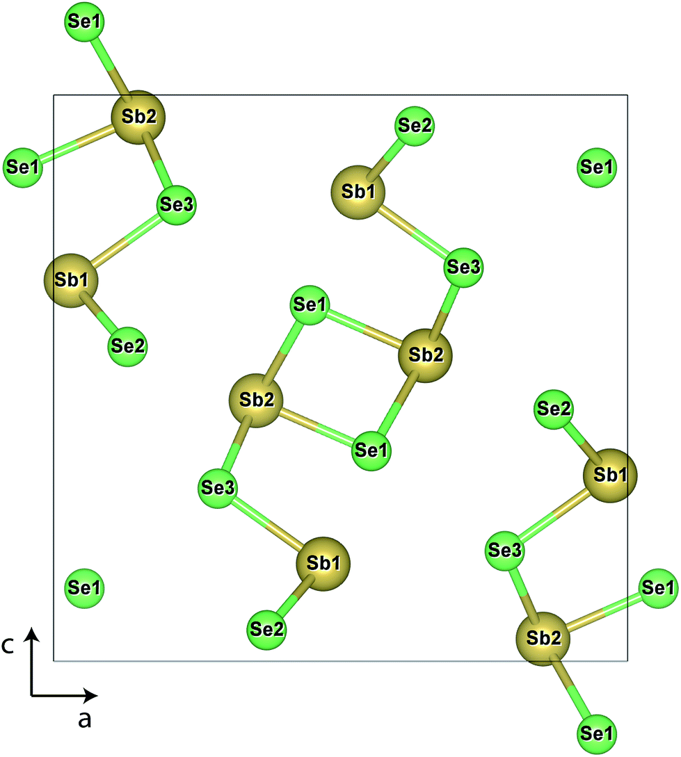 | ||
| Fig. 1 Crystal structure of Sb2Se3, with individual site labels. Antimony atoms are depicted in gold and selenium in light green. | ||
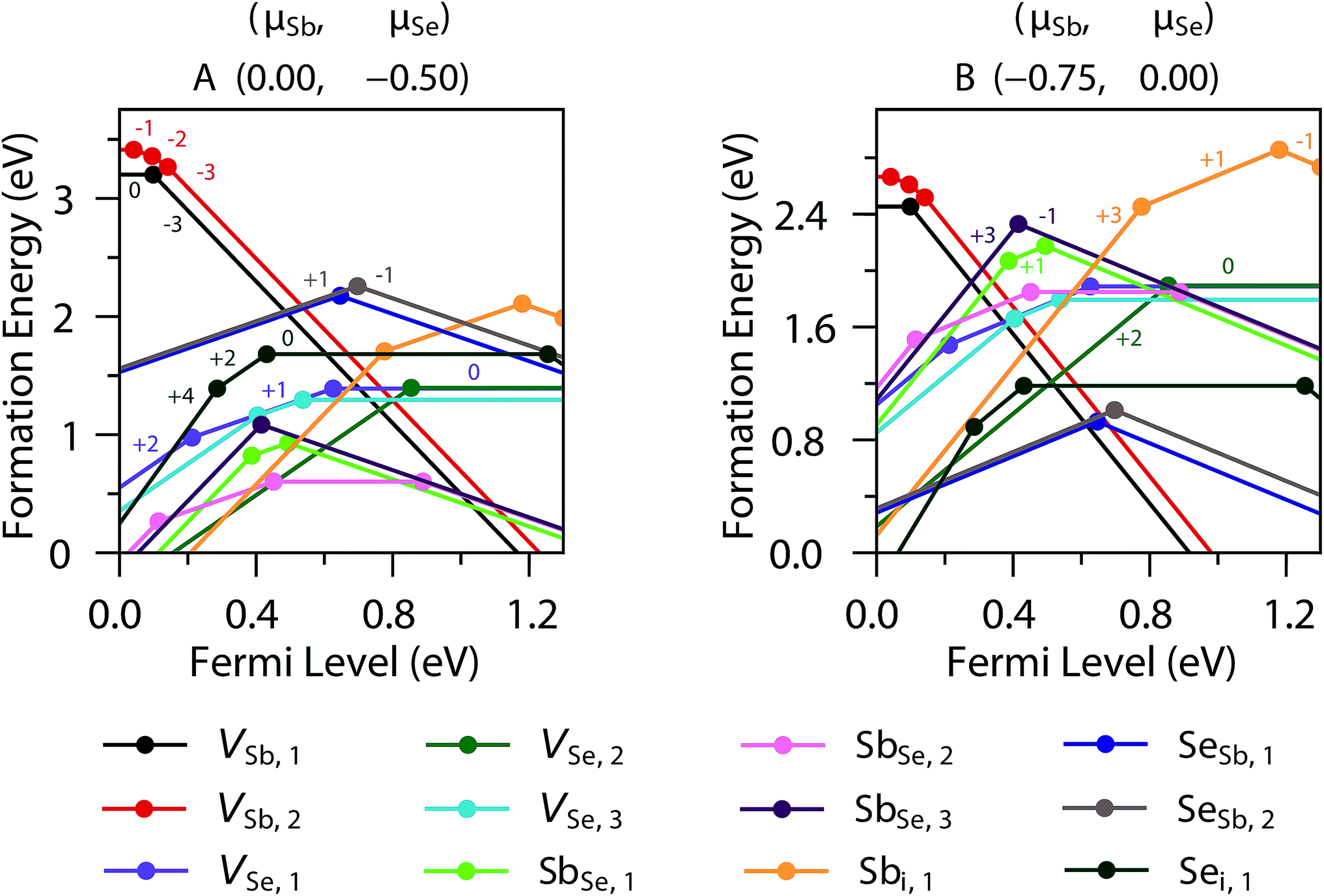 | ||
| Fig. 2 Defect transition level diagram for Sb2Se3 under limiting chemical potential conditions ((A) Sb-rich; (B) Se-rich), plotting defect formation energy (eV) against position of Fermi level above the VBM. Defect labels are given in the legend, charge states are given by labels adjacent to lines, with lines of the same slope representing the same charge state, and transition levels are represented by the filled dots. | ||
In the Se-rich regime, however, many of these previously problematic defects are moved to higher formation energies. While the neutral charge states of both VSb remain high in formation energy, the −3 charge states are relevant elsewhere in the Fermi level range – they intercept the +1 charge states for each SeSb antisite in the middle of the gap; again these will act to compensate each other and likely pin the Fermi level mid-gap (∼0.62 eV above the VBM). For this Fermi level position, far fewer defects have a formation energy below 1.5 eV: only the SeSb and VSb already noted, in addition to the Se interstitial. Of these, Sei has multiple transition levels deep within the band gap, that could plausibly act as hole or electron traps. VSb acts as a deep acceptor, with all transition levels lying close to, but further than 0.025 eV from, the VB edge; the separation by site reveals that the −2 and −1 charge states are stabilised for VSb,2, which has a more regular coordination environment, compared to VSb,1, where only the (−3/0) transition level is observed. Both SeSb defects however, are amphoteric, with an ultra-deep (+1/−1) transition level; lying in the middle of the gap, these are particularly likely to act as recombination centres, as they will likely have similar carrier capture cross-sections for both electrons and holes, and thus are potentially highly detrimental to photovoltaic performance.
To attempt to validate some of these results, we can compare the positions of these expected trap states with those found in a recent DLTS study of Tang and co-workers on cells produced by RTE and vapour transport deposition;16 in both cases, the traps were observed to appear in similar positions albeit with different densities. Comparing to the vapour transport deposition values first, the two hole traps lie at 0.48 ± 0.07 eV and 0.71 ± 0.02 eV above the valence band maximum – these align almost exactly with our calculated HSE06+D3 (+1/−1) TLs of SbSe,1 (VBM + 0.494 eV) and SeSb,2 (VBM + 0.697 eV) respectively. A similar agreement is found with the RTE-synthesised cell DLTS values too (the hole traps lying at 0.49 ± 0.03 eV and 0.74 ± 0.04 eV above the valence band maximum) and these are represented pictorially in the Fig. 3. A recent study found that variation of ionization energies with temperature can cause disparities between defect transition levels and the actual likely activation energies seen in experimental DLTS studies in GaN (highly dependent on the defect itself – for 300 K, a variation of ∼60 meV was seen for VGa–ON–2H, while a significant ∼250 meV shift was seen for CN),31 and as such this agreement between our simulations and DLTS could be fortuitous. In both prior, PBE-based defect studies of Sb2Se3, however, no transition levels align well with these DLTS levels, even considering a large temperature effect (neither study gives a possible hole trap within 0.3 eV of the 0.71 eV hole trap position, and the closest transition levels are at least 0.1 eV from the first hole trap) – this does seem to demonstrate the necessity for a hybrid functional, as well as a comprehensive study of all possible charge states to properly describe the material's complex defect chemistry. A recent study has found that even hybrid DFT energies, if based on defect geometries relaxed using standard DFT functionals, can lead to significant uncertainty in the defect level.19 For the electron trap (E1), a further level of uncertainty is introduced through the renormalization of the conduction band position with temperature – however, using the calculated gap of 1.300 eV for the position of the conduction band minimum (CBM) the trap (0.61 ± 0.03 eV below the CBM) is predicted to lie at essentially the same position as the second hole trap (H2), and as an amphoteric defect, SeSb,2 (CBM – 0.603 eV) is the most likely candidate for this trap also. The proposition that these may in fact be the same defect state is not too unlikely – its position near the middle of the gap could lead to very similar capture cross-sections for both holes and electrons,32 and E1 and H2 were found to have similar concentrations to each other for both sampled cells. While it is clear further validation may be necessary, both cation–anion and anion–cation intrinsic antisites seem to be the strongest candidates for the trap states in Sb2Se3, given our calculations.
 | ||
| Fig. 3 Defect transition level diagrams for Sb2Se3 with the position of the DLTS trap levels recorded by Wen et al. for (a) a VTD-synthesised and (b) a RTE-synthesised cell marked on, with the experimental uncertainty given by the bar width.16 Green bars represent the hole traps, and orange represents the electron trap, and the defect labels are identical to those in Fig. 2. The diagram is plotted at the Se-rich chemical potential limit, in accordance with Wen et al.’s expected synthesis conditions, however the actual chemical potential conditions during synthesis are difficult to determine and likely to be closer to stoichiometry than our extreme limits – as such, the formation energies are only loosely considered when identifying the trap states. | ||
4 Discussion
The identification of potential recombination centres at both chemical potential limits has implications not only for the use of Sb2Se3 as a solar absorber but also other applications that might utilise its high absorption, but also need specific purity, such as radiation detection. The detrimental effect of these trap states could be alleviated, however, by targeted passivation: an analogy might be made to another popular, earth abundant solar absorber, Cu2ZnSnS4 (CZTS), which had plateaued in efficiency due to a large Voc deficit – which some studies have related partly to intrinsic antisite defects or cation disorder, with varying reports of CuZn, CuSn or SnZn.33–35 Some improvement in CZTS cells has been observed, however, through targeted doping with Na, suppressing the effect of intrinsic defects, and increasing carrier lifetimes.36–38 For Sb2Se3, a possible strategy may be to favour Se-rich synthesis or treatments, combined with extrinsic doping on the Sb sites to suppress the formation of SeSb defects.Alternatively, we might note that the multiple deep acceptors and donors in both chemical potential limits suggest that Sb2Se3 will resist significant p or n-type doping, and that a more effective cell may be possible through synthesising Sb2Se3 as close to stoichiometry as possible, resulting in a compromise that maximises the formation of both antisite defects, and forming a p–i–n architecture with Sb2Se3 as an intrinsic layer. In this case, efforts may be necessary to find optimal contact materials to account for the limited accessible range in Fermi level.
As well as their potential impact on the photovoltaic behaviour of Sb2Se3, the presence of low formation energy, deep antisite defects bears discussion within the wider context of defects in functional energy materials. With the rise of the hybrid lead halide perovskites in PV, a number of publications have discussed the topic of ‘defect tolerance’39–41 in semiconductors, whereby materials are resistant to the formation of defects within them, or that such defects' detrimental effects are minimised. Some studies have directly linked defect tolerance with an electronic structure that has a VBM of antibonding character39,40 (demonstrated in materials with ns2 ‘lone pair’ cations such as Pb2+, Sb3+ or Bi3+)42–45 and a high dielectric constant. In our previous work, we found Sb2Se3 to possess both of these characteristic properties,8 however this study, along with the Voc deficit in cells, suggests that Sb2Se3 is far from defect tolerant. This is consistent with recent research suggesting that defect tolerance has significant dependence on other factors, such as crystal structure and cation valence.46,47 On the other hand, from a chemist's point of view, the presence of such cation–anion antisites in Sb2Se3 is perhaps not surprising – the amphoteric, ‘soft’ chemical behaviour of both antimony and selenium is well known, and thus the relative stability of such antisites, and multiple charge states therein, might naively be expected to be possible. Indeed, previous studies in the chemically-related bismuth tetradymite structures (Bi2Se3, Bi2Se2Te) found that cation–anion antisite defects were also low in formation energy and could act as limits to performance.48 Regardless, it is clear that close investigation of the defect behaviour of Sb2Se3 is necessary for its future usage in energy applications.
5 Conclusions
In this study, we have calculated the intrinsic defects in the candidate solar absorber Sb2Se3 using hybrid Density Functional Theory and including all defect sites to attempt to perform a complete assessment of its defect behaviour. We have found that, regardless of chemical potential limit, there will be low formation energy cation–anion anisite defects with mid-gap transition levels that could act as recombination centres. By noting the alignment of our calculated transition levels with published DLTS results, we propose that these SeSb and SbSe defects are most likely to be the trap states present in devices, and the potential barrier to improving device efficiencies. In order for Sb2Se3 to further improve as a useful optoelectronic material, it is critical that these defects must be suppressed, perhaps through targeted passivation by extrinsic dopants.Conflicts of interest
There are no conflicts of interest to declare.Acknowledgements
The authors would like to thank Dr Ben Williamson and Dr John Buckeridge for useful discussions. The authors acknowledge the use of the UCL Legion and Grace High Performance Computing Facility (Legion@UCL and Grace@UCL) in the production of this work. This work was also performed on the ARCHER UK National Supercomputing Service, via our membership of the UK's HEC Materials Chemistry Consortium, funded by EPSRC (EP/L000202). CNS is grateful to the Department of Chemistry at UCL for the provision of a DTA studentship (ref no. 1492829). DOS acknowledges support from the SUPERSOLAR Solar Energy Hub (EP/J017361/1), EPSRC (EP/N01572X/1), and membership of the Materials Design Network.References
- N. M. Haegel, R. Margolis, T. Buonassisi, D. Feldman, A. Froitzheim, R. Garabedian, M. Green, S. Glunz, H.-M. Henning, B. Holder, I. Kaizuka, B. Kroposki, K. Matsubara, S. Niki, K. Sakurai, R. A. Schindler, W. Tumas, E. R. Weber, G. Wilson, M. Woodhouse and S. Kurtz, Science, 2017, 356, 141–143 CrossRef CAS PubMed.
- L. M. Peter, Philos. Trans. R. Soc., A, 2011, 369, 1840–1856 CrossRef CAS PubMed.
- A. M. Ganose, C. N. Savory and D. O. Scanlon, Chem. Commun., 2017, 53, 20–44 RSC.
- Y. Zhou, L. Wang, S. Chen, S. Qin, X. Liu, J. Chen, D.-J. Xue, M. Luo, Y. Cao, Y. Cheng, E. H. Sargent and J. Tang, Nat. Photonics, 2015, 9, 409–415 CrossRef CAS.
- M. R. Filip, C. E. Patrick and F. Giustino, Phys. Rev. B: Condens. Matter Mater. Phys., 2013, 87, 205125 CrossRef.
- J. J. Carey, J. P. Allen, D. O. Scanlon and G. W. Watson, J. Solid State Chem., 2014, 213, 116–125 CrossRef CAS.
- B. Blank, T. Kirchartz, S. Lany and U. Rau, Phys. Rev. Appl., 2017, 8, 024032 CrossRef.
- L. J. Phillips, C. N. Savory, O. S. Hutter, P. J. Yates, H. Shiel, S. Mariotti, L. Bowen, M. Birkett, K. Durose, D. O. Scanlon and J. D. Major, IEEE J. Photovolt., 2018, 9, 544–551 Search PubMed.
- S. Messina, M. T. S. Nair and P. K. Nair, J. Electrochem. Soc., 2009, 156, H327–H332 CrossRef CAS.
- S.-J. Moon, Y. Itzhaik, J.-H. Yum, S. M. Zakeeruddin, G. Hodes and M. Grätzel, J. Phys. Chem. Lett., 2010, 1, 1524–1527 CrossRef CAS.
- N. Guijarro, T. Lutz, T. Lana-Villarreal, F. O'Mahony, R. Gómez and S. A. Haque, J. Phys. Chem. Lett., 2012, 3, 1351–1356 CrossRef CAS.
- Y. C. Choi, T. N. Mandal, W. S. Yang, Y. H. Lee, S. H. Im, J. H. Noh and S. I. Seok, Angew. Chem., Int. Ed., 2014, 53, 1329–1333 CrossRef CAS.
- Z. Li, X. Liang, G. Li, H. Liu, H. Zhang, J. Guo, J. Chen, K. Shen, X. San, W. Yu, R. E. I. Schropp and Y. Mai, Nat. Commun., 2019, 10, 125 CrossRef PubMed.
- D.-B. Li, X. Yin, C. R. Grice, L. Guan, Z. Song, C. Wang, C. Chen, K. Li, A. J. Cimaroli, R. A. Awni, D. Zhao, H. Song, W. Tang, Y. Yan and J. Tang, Nano Energy, 2018, 49, 346–353 CrossRef CAS.
- G. Li, Z. Li, X. Liang, C. Guo, K. Shen and Y. Mai, ACS Appl. Mater. Interfaces, 2018, 11, 828–834 CrossRef.
- X. Wen, C. Chen, S. Lu, K. Li, R. Kondrotas, Y. Zhao, W. Chen, L. Gao, C. Wang, J. Zhang, G. Niu and J. Tang, Nat. Commun., 2018, 9, 2179 CrossRef.
- M. A. Tumelero, R. Faccio and A. A. Pasa, J. Phys. Chem. C, 2016, 120, 1390–1399 CrossRef CAS.
- X. Liu, X. Xiao, Y. Yang, D.-J. Xue, D.-B. Li, C. Chen, S. Lu, L. Gao, Y. He, M. C. Beard, G. Wang, S. Chen and J. Tang, Prog. Photovoltaics, 2017, 25, 861–870 CAS.
- J. D. Gouveia and J. Coutinho, Electronic Structure, 2019, 1, 015008 CrossRef.
- G. Kresse and J. Hafner, Phys. Rev. B: Condens. Matter Mater. Phys., 1993, 47, 558–561 CrossRef CAS.
- G. Kresse and J. Hafner, Phys. Rev. B: Condens. Matter Mater. Phys., 1994, 49, 14251–14269 CrossRef CAS.
- G. Kresse and J. Furthmüller, Phys. Rev. B: Condens. Matter Mater. Phys., 1996, 54, 11169–11186 CrossRef CAS.
- G. Kresse and J. Furthmüller, Comput. Mater. Sci., 1996, 6, 15–50 CrossRef CAS.
- A. V. Krukau, O. A. Vydrov, A. F. Izmaylov and G. E. Scuseria, J. Chem. Phys., 2006, 125, 224106 CrossRef PubMed.
- S. Grimme, J. Comput. Chem., 2004, 25, 1463–1473 CrossRef CAS.
- M. Birkett, W. M. Linhart, J. Stoner, L. J. Phillips, K. Durose, J. Alaria, J. D. Major, R. Kudrawiec and T. D. Veal, APL Mater., 2018, 6, 084901 CrossRef.
- C. Freysoldt, J. Neugebauer and C. G. Van de Walle, Phys. Rev. Lett., 2009, 102, 016402 CrossRef PubMed.
- S. Lany and A. Zunger, Phys. Rev. B: Condens. Matter Mater. Phys., 2008, 78, 235104 CrossRef.
- S. T. Murphy and N. D. M. Hine, Phys. Rev. B: Condens. Matter Mater. Phys., 2013, 87, 094111 CrossRef.
- K. Momma and F. Izumi, J. Appl. Crystallogr., 2011, 44, 1272–1276 CrossRef CAS.
- D. Wickramaratne, C. E. Dreyer, B. Monserrat, J.-X. Shen, J. L. Lyons, A. Alkauskas and C. G. V. de Walle, Appl. Phys. Lett., 2018, 113, 192106 CrossRef.
- J. E. Lowther, J. Phys. C: Solid State Phys., 1980, 13, 3681–3696 CrossRef CAS.
- D. Han, Y. Y. Sun, J. Bang, Y. Y. Zhang, H.-B. Sun, X.-B. Li and S. B. Zhang, Phys. Rev. B: Condens. Matter Mater. Phys., 2013, 87, 155206 CrossRef.
- S. Chen, A. Walsh, X.-G. Gong and S.-H. Wei, Adv. Mater., 2013, 25, 1522–1539 CrossRef CAS.
- S. Kim, J.-S. Park and A. Walsh, ACS Energy Lett., 2018, 3, 496–500 CrossRef CAS.
- T. Gershon, Y. S. Lee, R. Mankad, O. Gunawan, T. Gokmen, D. Bishop, B. McCandless and S. Guha, Appl. Phys. Lett., 2015, 106, 123905 CrossRef.
- T. Gershon, B. Shin, N. Bojarczuk, M. Hopstaken, D. B. Mitzi and S. Guha, Adv. Energy Mater., 2015, 5, 1400849 CrossRef.
- D. Tiwari, T. Koehler, X. Lin, R. Harniman, I. Griffiths, L. Wang, D. Cherns, R. Klenk and D. J. Fermin, Chem. Mater., 2016, 28, 4991–4997 CrossRef CAS.
- R. E. Brandt, V. Stevanović, D. S. Ginley and T. Buonassisi, MRS Commun., 2015, 5, 265–275 CrossRef CAS.
- A. Zakutayev, C. M. Caskey, A. N. Fioretti, D. S. Ginley, J. Vidal, V. Stevanovic, E. Tea and S. Lany, J. Phys. Chem. Lett., 2014, 5, 1117–1125 CrossRef CAS PubMed.
- A. Walsh and A. Zunger, Nat. Mater., 2017, 16, 964–967 CrossRef CAS PubMed.
- A. Walsh, D. J. Payne, R. G. Egdell and G. W. Watson, Chem. Soc. Rev., 2011, 40, 4455–4463 RSC.
- K. K. Bass, L. Estergreen, C. N. Savory, J. Buckeridge, D. O. Scanlon, P. I. Djurovich, S. E. Bradforth, M. E. Thompson and B. C. Melot, Inorg. Chem., 2017, 56, 42–45 CrossRef CAS PubMed.
- A. M. Ganose, S. Matsumoto, J. Buckeridge and D. O. Scanlon, Chem. Mater., 2018, 30, 3827–3835 CrossRef CAS PubMed.
- T. L. Hodgkins, C. N. Savory, K. K. Bass, B. L. Seckman, D. O. Scanlon, P. I. Djurovich, M. Thompson and B. Melot, Chem. Commun., 2019, 55, 3164–3167 RSC.
- R. E. Brandt, J. R. Poindexter, P. Gorai, R. C. Kurchin, R. L. Z. Hoye, L. Nienhaus, M. W. B. Wilson, J. A. Polizzotti, R. Sereika, R. Žaltauskas, L. C. Lee, J. L. MacManus-Driscoll, M. Bawendi, V. Stevanović and T. Buonassisi, Chem. Mater., 2017, 29, 4667–4674 CrossRef CAS.
- R. C. Kurchin, P. Gorai, T. Buonassisi and V. Stevanović, Chem. Mater., 2018, 30, 5583–5592 CrossRef CAS.
- D. O. Scanlon, P. D. C. King, R. P. Singh, A. de la Torre, S. M. Walker, G. Balakrishnan, F. Baumberger and C. R. A. Catlow, Adv. Mater., 2012, 24, 2154–2158 CrossRef CAS PubMed.
Footnote |
| † Electronic supplementary information (ESI) available: Lattice parameter comparison, theoretical defect formalism, thermodynamic transition levels. See DOI: 10.1039/c9ta02022e |
| This journal is © The Royal Society of Chemistry 2019 |