
 Open Access Article
 This Open Access Article is licensed under a
 Creative Commons Attribution 3.0 Unported Licence
Cu:NiO as a hole-selective back contact to improve the photoelectrochemical performance of CuBi2O4 thin film photocathodes†
Angang
Song
 ab,
Paul
Plate
a,
Abdelkrim
Chemseddine
a,
Fuxian
Wang
a,
Fatwa F.
Abdi
a,
Markus
Wollgarten
c,
Roel
van de Krol
ab and
Sean P.
Berglund
*a
ab,
Paul
Plate
a,
Abdelkrim
Chemseddine
a,
Fuxian
Wang
a,
Fatwa F.
Abdi
a,
Markus
Wollgarten
c,
Roel
van de Krol
ab and
Sean P.
Berglund
*a
aInstitute for Solar Fuels, Helmholtz-Zentrum Berlin für Materialien und Energie GmbH, Hahn-Meitner-Platz 1, 14109 Berlin, Germany. E-mail: sean.berglund@helmholtz-berlin.de
bInstitute für Chemie, Technische Universität Berlin, Straße des 17. Juni 124, 10623 Berlin, Germany
cDepartment Nanoscale Structures and Microscopic Analysis, Helmholtz-Zentrum Berlin für Materialien und Energie GmbH, Hahn-Meitner-Platz 1, 14109 Berlin, Germany
First published on 20th March 2019
Abstract
P-type CuBi2O4 has recently been reported as a promising photocathode material for photoelectrochemical water reduction due to its optimal optical band gap and positive photocurrent onset potential. However, despite these favourable attributes, CuBi2O4 photocathodes have shown limitations in charge carrier transport within CuBi2O4 and across the interface with n-type fluorine doped tin oxide (FTO). To overcome the later limitation, a very thin and transparent p-type Cu doped NiO (Cu:NiO) back contact layer is inserted between the FTO substrate and CuBi2O4. The Cu:NiO layer is prepared by electron beam evaporation of Ni and Cu followed by post annealing in air. CuBi2O4 photocathodes with a 7 nm thick Cu:NiO back contact layer produce photocurrent densities up to 2.83 mA cm−2 at 0.6 V versus RHE under back illumination with H2O2 as an electron scavenger, which is 25% higher than photocathodes without the back contact layer. This is also the highest reported photocurrent density for CuBi2O4 to date. The observed improvement in photocurrent density with the Cu:NiO back contact layer is attributed to hole selective transport across the CuBi2O4–Cu:NiO interface with a decrease in barrier height compared to the CuBi2O4–FTO interface.
Introduction
CuBi2O4, a p-type semiconductor material, has recently attracted attention as a photocathode material due to several favourable attributes for photoelectrochemical water splitting. First, it is reported to have an optimal optical bandgap in the range of 1.5–1.8 eV,1–5 which is the ideal range for the top absorber layer in a dual absorber photoelectrochemical device with maximum utilization of the AM1.5 solar spectrum.6,7 Second, its conduction band is estimated to be at a more negative potential than the thermodynamic potential for water reduction to enable solar H2 production.8–11 Third, its Fermi level is located at a more positive potential (>1.0 V vs. RHE) than many other p-type photocathode materials such as Cu2O, CuFeO2 and p-type Si,12–17 which is important for the photocathode to generate adequate photovoltage in a dual absorber device.Despite all these favourable attributes, there are several limitations that must be overcome to make CuBi2O4 more efficient as a photocathode for water reduction. One of the biggest limitations is the relatively poor charge carrier transport of photogenerated electrons and holes within CuBi2O4, which is a common problem for metal oxide photoelectrode materials.10,12,17,18 Previously, we improved the charge carrier transport in CuBi2O4 thin film photocathodes by using gradient self-doping to create an internal electric field,19 significantly improving the charge separation efficiency and overall photoelectrochemical performance. Another limitation of CuBi2O4 thin film photocathodes is the hindered hole transport across the CuBi2O4–substrate interface when n-type fluorine doped tin oxide (FTO) is used as the substrate. For p-type photocathode materials, such as CuBi2O4, the minority carriers (electrons) must be transferred to the redox species at the semiconductor–electrolyte interface to drive the photoelectrochemical reduction reaction while the majority carriers (holes) must be separated and transported across the semiconductor–substrate interface. FTO has a reported work function of 4.8–5.0 eV vs. vacuum (0.3–0.5 V vs. RHE),20–22 which is well positioned to form an ohmic contact with respect to the Fermi level of many n-type photoanode materials. However, p-type CuBi2O4 has a much more positive Fermi level at 5.71–5.93 eV vs. vacuum (1.21–1.43 V vs. RHE).10,19 This mismatch between the work function of degenerately doped FTO and the Fermi level of CuBi2O4 can result in the formation of a Schottky barrier at the CuBi2O4–FTO interface impeding hole transport.23,24 Additionally, defect states can lead to recombination at the interface, which has been observed for other metal oxide semiconductors deposited directly on conducting substrates.25–27 The application of a more favourable back-contact layer as compared to FTO or the modification of the FTO–CuBi2O4 interface could therefore potentially improve the photoelectrochemical performance of CuBi2O4 photocathodes.
Nickel oxide (NiO) is a p-type semiconductor, that has been used as back contact layer in various electrical and photovoltaic devices, including electrochromic devices, organic light emitting diodes, organic photovoltaics, and organic–inorganic perovskite solar cells due to its acceptable conductivity, high transparency, and suitable Fermi level of 5.0–5.6 eV (0.5–1.1 V vs. RHE).28–30 It has been shown that the p-type conductivity of NiO can be improved with Cu doping so that Cu doped NiO (Cu:NiO) can act as an effective hole selective back contact with lower resistance to hole transport.26 These properties are also desired in a back contact layer for p-type photocathode materials, such as CuBi2O4, where holes must be extracted at the semiconductor–substrate interface.27,31 In this work, we therefore introduced a very thin Cu:NiO layer at the FTO–CuBi2O4 interface as an ideal back contact material for CuBi2O4. In the following section we confirm this by showing that CuBi2O4 photocathodes with a very thin Cu:NiO back contact layer have lower electrical resistivity, higher charge carrier separation efficiency, and higher photocurrent density due to improved band energy alignment.
Results and discussion
Photoelectrochemical and optical properties
Photoelectrochemical measurements were performed systematically by varying the thicknesses of the CuBi2O4 film and the inserted Cu:NiO back contact layer in order to optimize the performance of CuBi2O4 photocathodes. The CuBi2O4 photocathodes were tested as working electrodes in a photoelectrochemical cell under simulated AM1.5 illumination. Fig. 1a shows representative chopped (dark/light) linear sweep voltammetry (LSV) scans for an optimized CuBi2O4 film synthesized on top of FTO and FTO/Cu:NiO substrates. The thickness of the Cu:NiO and CuBi2O4 films were approximately 7 nm and 260 nm, respectively. The measurements were performed in 0.3 M K2SO4 and 0.2 M phosphate buffer (pH 6.65) with H2O2 added as an electron scavenger to test the CuBi2O4 photocathodes without surface recombination or limitations in the reaction kinetics. For water oxidation and reduction experiments (i.e., without an electron scavenger), argon bubbling was used to remove dissolved O2 and to test for activity towards proton reduction. In Fig. 1a, the photocurrent density is clearly higher in magnitude for the FTO/Cu:NiO/CuBi2O4 photocathode compared to the FTO/CuBi2O4 photocathode. With an optimal CuBi2O4 thickness of 260 nm the FTO/Cu:NiO/CuBi2O4 photocathode produces photocurrent densities of −0.5 mA cm−2 and −2.83 mA cm−2 at 0.6 V versus RHE under backside illumination without and with H2O2 as an electron scavenger, respectively. This is an improvement of 22% and 25% with Ar bubbling and H2O2, respectively, compared to the FTO/CuBi2O4 photocathode. The improvement was consistent for both frontside and backside illumination (see Fig. S1†) and held for a range of CuBi2O4 film thicknesses between 150 and 380 nm as shown in the inset of Fig. 1a (see Fig. S2a and b† for the individual LSV scans for different CuBi2O4 film thicknesses). To rule out the possibility that additional photocurrent density comes from the Cu:NiO layer, chopped LSV measurements were performed on a FTO/Cu:NiO substrate (34 nm of Cu:NiO) without CuBi2O4 (see Fig. S3†). The photocurrent density of the FTO/Cu:NiO sample (5 × 10⁻⁴ mA cm−2 at 0.4 V vs. RHE under backside illumination) is barely distinguishable from the dark current density. In addition, increasing the thickness of the Cu:NiO layer in the FTO/Cu:NiO/CuBi2O4 photocathode actually decreases the photocurrent density, as shown in Fig. S4.† These results provide strong evidence that the additional photocurrent is not produced by the Cu:NiO layer. Instead the improvement in performance for the FTO/Cu:NiO/CuBi2O4 photocathode is due to electronic interactions between the FTO, Cu:NiO, and CuBi2O4 layers, as will be shown in the remainder of this article.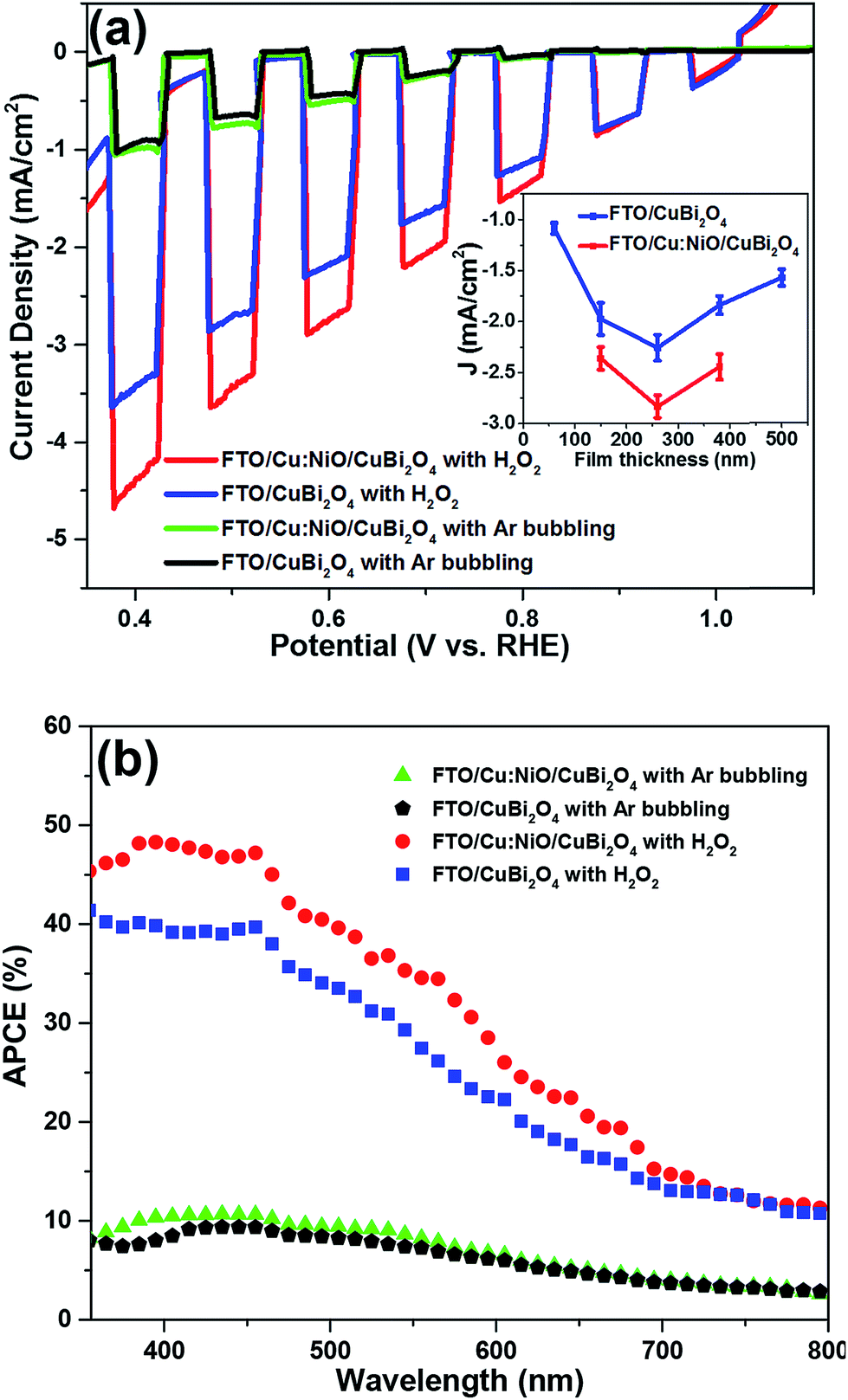 | ||
| Fig. 1 (a) Chopped LSV scans for CuBi2O4 photocathodes synthesized to a thickness of ∼260 nm on FTO and on FTO/Cu:NiO substrates. Inset shows the average photocurrent densities (at least 3 samples) at 0.6 V vs. RHE extracted from LSV scans for photocathodes with different thicknesses (see Fig. S2† for LSV scans). (b) APCE spectra of CuBi2O4 on FTO (blue squares and black pentagons), CuBi2O4 on FTO/Cu:NiO (red circles and green triangles) in 0.3 M K2SO4 and 0.2 M phosphate buffer (pH 6.65) with Ar bubbling and with H2O2 at a potential of 0.6 V vs. RHE. All measurements were performed under backside illumination. | ||
To gain additional information about the enhancement mechanism of the Cu:NiO back contact, we measured the incident photon-to-current conversion efficiency (IPCE). Combining this with the optical absorption we then calculated the absorbed photon-to-current efficiency (APCE) of the FTO/CuBi2O4 and FTO/Cu:NiO/CuBi2O4 photocathodes with and without H2O2. These results are shown in Fig. S5† and 1b for an applied potential of 0.6 V vs. RHE. With H2O2 the IPCE and APCE values are significantly higher for the FTO/Cu:NiO/CuBi2O4 photocathode for UV light (≤400 nm) and for visible light (400–700 nm). As an effective electron scavenger, H2O2 is expected to eliminate surface recombination and prevent limitations in reaction kinetics at the semiconductor–liquid interface. Therefore, these APCE values represent the overall charge separation efficiency within the solid-state regions of the photocathodes. Since the FTO/Cu:NiO/CuBi2O4 photocathode has consistently higher APCE values than the FTO/CuBi2O4 photocathode for all wavelengths, it can be inferred that the Cu:NiO back contact layer improves the overall charge separation within the individual thin films and/or across the solid-state interfaces.
The IPCE values can also be used to calculate the predicted AM1.5 photocurrent density (JAM1.5) according to eqn (4) in the Experimental section. The JAM1.5 values are 3.07 mA cm−2 and 2.55 mA cm−2 at 0.6 VRHE for the FTO/Cu:NiO/CuBi2O4 and FTO/CuBi2O4 photocathodes, respectively, which are very close to the values of 2.83 mA cm−2 and 2.26 mA cm−2 obtained for the chopped LSV measurements under AM1.5 solar simulation.
Lastly, the FTO/CuBi2O4 and FTO/Cu:NiO/CuBi2O4 photocathodes were compared in terms of photoelectrochemical stability. Fig. S7† shows dark/light constant potential measurements for the photocathodes in 0.3 M K2SO4 and 0.2 M phosphate buffer (pH 6.65) with Ar bubbling and with H2O2 added at 0.6 V vs. RHE. With Ar bubbling both photocathodes show a fast, initial decay in photocurrent (∼50% within 15 min) due to photo-corrosion of CuBi2O4, which is a common challenge for metal oxide photocathodes containing copper.10,12 To address this challenge, strategies such as conformal protection layers with co-catalysts can be utilised.15,19,31 With H2O2 added the FTO/CuBi2O4 and FTO/Cu:NiO/CuBi2O4 photocathodes still show a drop in photocurrent but the decay is much slower (∼50% in 120 min) and the FTO/Cu:NiO/CuBi2O4 photocathode shows significantly higher photocurrent for the entire period of time, which further validates the effectiveness of Cu:NiO as a back contact layer for CuBi2O4.
The APCE values shown in Fig. 1b, which were calculated using optical absorption of the entire photocathodes, provide compelling evidence that the improvement in photoactivity of the FTO/Cu:NiO/CuBi2O4 photocathode is not due to an optical effect of the Cu:NiO layer. In fact the very thin Cu:NiO layer has only a minor influence on the overall optical absorption. Fig. 2 shows the absorptance spectra for a bare glass substrate along with a 7 nm Cu:NiO film, a 260 nm CuBi2O4 film, and a 7 nm/260 nm Cu:NiO/CuBi2O4 film stack, all deposited on top of glass substrates. Fig. S8† shows the absorptance spectrum of a bare FTO substrate along with that of FTO/Cu:NiO, FTO/CuBi2O4 and FTO/Cu:NiO/CuBi2O4 photocathodes. These spectra show that the absorptance values are only slightly higher for the Cu:NiO/CuBi2O4 layering compared to CuBi2O4, regardless of whether the substrate is glass or FTO. For the hypothetical condition of 100% APCE under AM1.5 illumination, the maximum obtainable increases in photocurrent density due to the slightly higher absorption are calculated to be 8.4% and 2.0% using the spectra in Fig. 2 and S8,† respectively. Recall that the measured increase in photocurrent density is much larger at 22–25% (see Fig. 1a). Clearly the increased photocurrent density is due to additional photophysical processes besides slightly higher optical absorption of the Cu:NiO/CuBi2O4 layering. Moreover, the increased optical absorption likely only occurs in the Cu:NiO layer rather than the CuBi2O4 layer, especially when backside illumination is used. At longer wavelengths the Cu:NiO layer may undergo free carrier absorption, which commonly occurs in highly doped metal oxide semiconductors used as transparent conducing oxides (TCOs).32–34 Similar to the FTO coated glass (bare FTO in Fig. S7†) the Cu:NiO coated glass sample (Cu:NiO in Fig. 1a) shows a low baseline absorptance of 5–10% that extends to energies that are much lower than the reported bandgap of NiO (3.6–4.3 eV or 288–344 nm light).30,35 Fig. S9a and b† show the transflectance spectra and direct bandgap Tauc plots for Cu:NiO films of different thicknesses of 7, 34 and 102 nm. The Tauc plots of the Cu:NiO films indicate that the bandgap is ∼3.75 eV (corresponding to 330 nm light). Fig. S9c† shows a Tauc plot of bare FTO substrate indicating a bandgap of ∼3.7 eV (corresponding to 335 nm light).
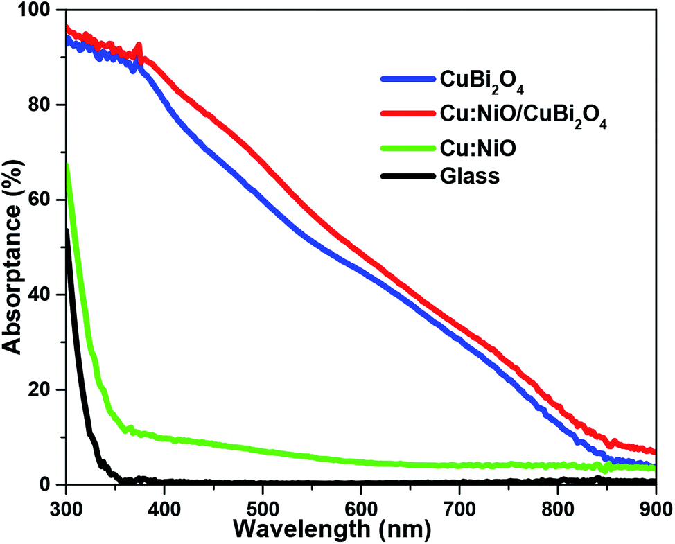 | ||
| Fig. 2 UV-vis absorptance spectra for a bare glass substrate (black line) along with a 7 nm Cu:NiO film (green line), a 260 nm CuBi2O4 film (blue line) and a 7 nm/260 nm Cu:NiO/CuBi2O4 film stack (red line), all deposited on top of glass. | ||
Crystal structure and morphology
The crystal structure and morphology of the CuBi2O4 thin film photocathodes and the individual FTO, Cu:NiO, and CuBi2O4 layers were investigated because crystal structure, crystallite orientation, nanostructure, and surface area can have a significant influence on the photoelectrochemical performance. The Cu:NiO intermediate layer can also influence the growth of CuBi2O4 during synthesis. Fig. 3 shows the SEM images of a bare FTO substrate, a 7 nm thick Cu:NiO layer deposited on FTO, a 260 nm thick CuBi2O4 film deposited on FTO, and a 7 nm/260 nm Cu:NiO/CuBi2O4 film stack. It also shows a cross-section transmission electron microscopy TEM image of a Cu:Ni film as deposited on FTO and after thermal oxidation to form a Cu:NiO film. Fig. 3a shows that the FTO surface is composed of angular crystal facets on the order of 10–500 nm, which is typical for fluorine doped tetragonal SnO2.36 Close examination of Fig. 3b reveals that the Cu:NiO layer is composed of small particles that cover the FTO facets. The CuBi2O4 films appear similar in Fig. 3c (on FTO) and Fig. 3d (on 7 nm Cu:NiO), indicating that the underlying Cu:NiO does not significantly alter the morphology of the deposited CuBi2O4 thin film. Fig. 3e shows a cross-sectional TEM image of the as-deposited Cu:Ni film. The thickness of the Cu:Ni layer is ∼4.2 nm, which is very close to the expected value of 4.4 nm (2 nm Ni/0.4 nm Cu/2 nm Ni) based on the QCM monitoring during deposition. Fig. 3f shows a corresponding TEM image of a Cu:Ni film that was annealed to form Cu:NiO. Annealing changes the morphology of the layer and increases the thickness slightly due to the incorporation of oxygen to form the NiO crystal structure. The mean thickness of the Cu:NiO in the TEM image matches the expected value of about 7 nm (estimated using the molar masses and mass densities of Ni and NiO with a starting thickness of 4 nm for the Ni metal). | ||
| Fig. 3 SEM images of a (a) bare FTO substrate, (b) 7 nm Cu:NiO deposited on FTO, (c) 260 nm CuBi2O4 deposited on FTO, (d) 260 nm CuBi2O4 deposited on 7 nm Cu:NiO on FTO. Cross-section TEM images of (e) 4.4 nm Cu:Ni film as deposited on FTO and (f) after annealing at 450 °C in air to form Cu:NiO. | ||
The surfaces of the FTO/CuBi2O4 and FTO/Cu:NiO/CuBi2O4 photocathodes were compared using atomic force microscopy (AFM) as shown in Fig. 4. AFM reveals that the root mean squared (RMS) roughness and real surface area of CuBi2O4 films deposited directly on FTO are 90 nm and 30 μm2, respectively. For CuBi2O4 films deposited on FTO/Cu:NiO the RMS roughness and real surface area are 82 nm and 30 μm2, respectively, so the FTO/Cu:NiO/CuBi2O4 photocathode has a slightly lower surface roughness than the FTO/CuBi2O4. This may be due to the underlying Cu:NiO layer smoothing out the sharp peaks and trenches of the FTO surface as the RMS surface roughness is 60 nm for the FTO/Cu:NiO substrate compared to 92 nm for bare FTO (see Fig. S10a and b in the ESI†). All substrates and deposited films show a similar real surface areas in the range of 28–31 μm2 for a cross-sectional area of 5 μm × 5 μm. Therefore the higher photocurrent density of the FTO/Cu:NiO/CuBi2O4 photocathode is not due to an increase in roughness or surface area.
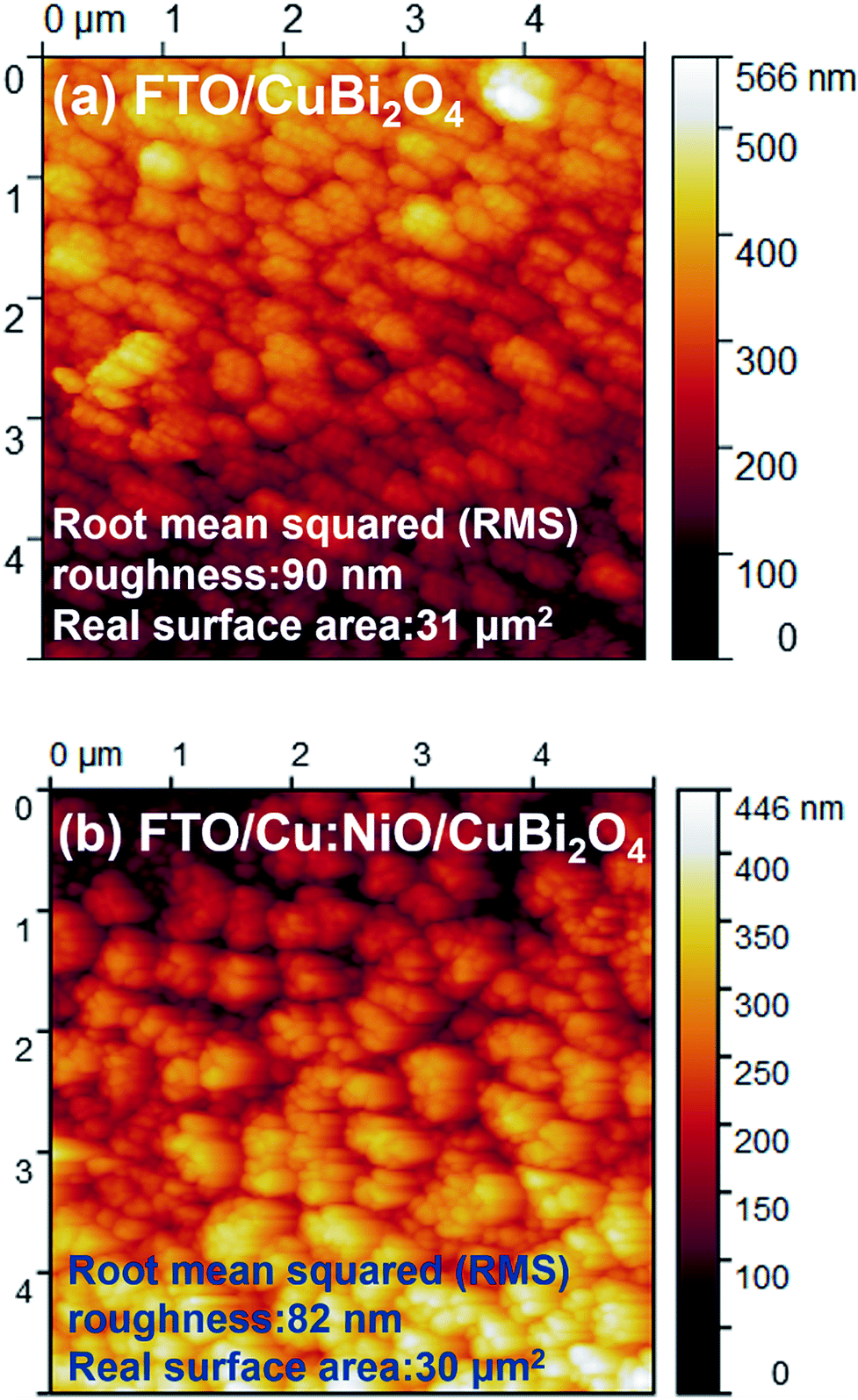 | ||
| Fig. 4 AFM images of CuBi2O4 thin films deposited on (a) a FTO substrate and (b) a 7 nm Cu:NiO layer on FTO. | ||
The crystallinity and chemical composition of each deposited layer was confirmed using X-ray diffraction (XRD) and energy-dispersive X-ray (EDX) measurements. Fig. 5a shows the X-ray diffractograms of Cu:NiO thin films with thicknesses of 7, 34, and 102 nm deposited on glass substrates along with that for a bare glass substrate. The diffractogram of the 102 nm Cu:NiO thin film (blue line) mainly exhibits the crystal structure of cubic nickel oxide (NiO, JCPDS 47-1049). However, two small peaks are also visible for monoclinic cupric oxide (CuO, JCPDS 48-1548). No metallic Cu or Ni peaks were observed and neither were any Cu2O peaks, indicating that the deposited film was fully oxidized. This is in agreement with the phase diagram of copper oxide, which shows that CuO is a stable phase at the annealing temperature of 450 °C in air at atmospheric pressure.37 In the diffractogram for the 34 nm Cu:NiO thin film (green line) no peaks are visible for the CuO phase. This may be due to the amount of CuO being too low or it could be due to the Cu more easily diffusing into the 34 nm NiO film compared to the 102 nm film. The 7 nm Cu:NiO thin film was also measured by XRD (magenta line) but no peaks could be discerned from the background signal. Fig. 5b shows the X-ray diffractogram of a FTO/CuBi2O4 sample (blue line), FTO/Cu:NiO/CuBi2O4 sample (red line), and bare FTO substrate. Both of these CuBi2O4 films show strong XRD peaks at 20.95°,28.02°, 33.30° and 46.69°, which can be assigned to the (200), (211), (310), and (411) lattice planes of tetragonal CuBi2O4, respectively, according to the CuBi2O4 reference data (JCPDS 42-0334).38,39 Since the diffractograms are nearly the same for these samples the underlying Cu:NiO layer has no obvious influence on the crystal structure of the deposited CuBi2O4 film.
 | ||
| Fig. 5 XRD diffractograms for (a) a bare glass substrate (black line) and Cu:NiO thin films deposited on glass substrates with thicknesses of 7 nm (magenta line), 34 nm (green line), and 102 nm (blue line), and XRD diffractograms for (b) a bare FTO substrate (black line) and ∼260 nm CuBi2O4 deposited on a FTO substrate (blue line) and a 7 nm Cu:NiO layer on FTO (red line). | ||
The chemical composition of the prepared films was analysed by energy-dispersive X-ray (EDX) mapping of a representative film area on a FTO/CuBi2O4 photocathode. The relevant SEM images with EDX mapping overlays are shown in Fig. S11.† The EDX signals from Cu, O, Bi and Sn appear to be homogeneously distributed over the entire film area. EDX was also performed on the 7 nm Cu:NiO layer to confirm the presence of Cu and Ni as shown in Fig. S12.† From these EDX results the Cu to Ni atomic ratio is about 1 to 10, which is in agreement with the QCM measurements of the Cu and Ni thicknesses during electron beam evaporation.
Electronic and semiconductor properties
To analyse the electronic interactions between FTO, Cu:NiO, and CuBi2O4 we performed solid-state current density vs. voltage (J–V) measurements on FTO/CuBi2O4/FTO, FTO/Cu:NiO/FTO, and FTO/Cu:NiO/CuBi2O4/Cu:NiO/FTO samples. The samples were prepared by depositing Cu:NiO or CuBi2O4 layers over the trenches in laser-cut FTO and FTO/Cu:NiO substrates, which were then measured as illustrated in Fig. S14.† For these samples it is assumed that FTO behaves more like a metal than a semiconductor since it is degenerately doped. The work function of FTO (4.8–5.0 eV) is much different than the Fermi level of CuBi2O4 (5.71–5.93 eV) so a Schottky barrier should form at each FTO/CuBi2O4 interface.10,19,20 As a result the FTO/CuBi2O4/FTO sample should be composed of back-to-back Schottky diodes.40,41 Plots of the band bending behaviour of the back-to-back Schottky diodes at zero bias and under bias are depicted in the ESI (see Fig. S15†) along with the derivation of a mathematical model, based on thermionic-emission–diffusion theory, for the current density (J) through back-to-back Schottky diodes. Fig. 6a and b show the experimental J–V data for FTO/CuBi2O4/FTO, FTO/Cu:NiO/CuBi2O4/Cu:NiO/FTO, and FTO/Cu:NiO/FTO samples along with the fit lines for the FTO/CuBi2O4/FTO and FTO/Cu:NiO/FTO samples. Fig. 6c and d show the modified Richardson plots for the FTO/CuBi2O4/FTO and FTO/Cu:NiO/FTO samples at applied biases of ±1, ±2, and ±4 V, respectively, with linear fit lines. The modified Richardson plots were constructed by performing the J–V measurements at different temperatures (see Fig. S16a and b†). By simultaneously fitting the experimental data in both the J–V measurements and modified Richardson plots, the barrier height (ϕB0) at zero bias and ideality factor (n) can be determined for the FTO/CuBi2O4 and FTO/Cu:NiO interfaces and the reduced effective Richardson constant (A**) can be estimated for the CuBi2O4 and Cu:NiO layers. The ϕB0 value for the FTO/CuBi2O4 interface is determined to be 0.37–0.38 eV, which is significantly higher than that for the FTO/Cu:NiO interface (0.11 eV). Note that, the FTO/Cu:NiO/FTO sample shows a drastically higher current density (>10-fold vs. the FTO/CuBi2O4/FTO sample) that increases nearly linear with the applied voltage, indicating that the FTO/Cu:NiO contact is more ohmic in nature. This also explains the larger deviation of the fit line in Fig. 6b from the measured data around 0 V, as a Schottky barrier was assumed for the fit. | ||
| Fig. 6 J–V curves for (a) FTO/Cu:NiO/CuBi2O4/Cu:NiO/FTO (red triangles) and FTO/CuBi2O4/FTO (blue circles), and (b) FTO/Cu:NiO/FTO samples including J fit lines. Modified Richardson plots for (c) FTO/CuBi2O4/FTO and (d) FTO/Cu:NiO/FTO samples with linear fit lines. | ||
Fig. 6a also shows the experimental J–V data for the FTO/Cu:NiO/CuBi2O4/Cu:NiO/FTO sample. Unfortunately, due to the parallel presence of a direct interface between the FTO and the CuBi2O4 along the trench sidewalls (see Fig. S13d†), the combined FTO/Cu:NiO/CuBi2O4 interface in this sample could not be unambiguously fit with the model. Nevertheless, it is clear that this sample shows a higher current density than the FTO/CuBi2O4/FTO sample, which is consistent with the higher photocurrent density of the FTO/Cu:NiO/CuBi2O4 photocathode described in the previous section. Overall, the results in Fig. 6 provide direct evidence that the barrier for charge carrier transfer is significantly lower at the FTO/Cu:NiO interface as compared to the FTO/CuBi2O4 interface.
The Fermi levels of the FTO, Cu:NiO, and CuBi2O4 layers were determined using two different analytical methods (1) Mott–Schottky analysis and (2) ultraviolet photoelectron spectroscopy (UPS). Fig. 7a shows the Mott–Schottky plots for a FTO/CuBi2O4 photocathode measured at three different frequencies. All three curves have similar slopes with an extrapolated x-axis intercept of about 1.12 V vs. RHE, which can be used to estimate the flat-band potential (φfb). This value for φfb can then be used to estimate the Fermi level (EF) while taking into account the potential drop across the Helmholtz layer.42 From the slope of the Mott–Schottky plot the acceptor density (NA) is estimated to be ∼3.2 × 1018 cm−3, which places the Fermi level within 0.077 eV of the valence band. Considering the band gap energy of ∼1.5 eV, this places the conduction band at approximately −0.3 V vs. RHE, which is more negative than the electrochemical potential for water reduction. As a consequence, the CuBi2O4 thin films are thermodynamically capable of photoelectrochemical water reduction, which we recently demonstrated for a forward gradient self-doped CuBi2O4 photocathode with a CdS/TiO2 overlayer for protection against photocorrosion and Pt as a co-catalyst.19 The Mott–Schottky plot for CuBi2O4 photocathode deposited on 7 nm Cu:NiO was also measured, as shown in Fig. S18a.† The estimated φfb value is at about 1.17 V vs. RHE, which is slightly higher than for CuBi2O4 deposited directly on FTO. Fig. 7b shows the Mott–Schottky plot for a FTO/Cu:NiO sample with a Cu:NiO thickness of 34 nm. The x-axis intercept indicates a φfb value of 0.71 V vs. RHE and NA is calculated to be ∼4.6 × 1018 cm−3. This reasonably high NA value suggests that Cu doping is effective and the Fermi level is positioned close to the valence band. Fig. S18b† shows the Mott–Schottky plot for a bare FTO substrate revealing a flat-band potential of around 0.31 V vs. RHE (4.81 eV vs. vacuum), which closely matches the work function of FTO obtained using other analytical methods.20–22
 | ||
| Fig. 7 Mott–Schottky plot for (a) ∼260 nm CuBi2O4 on bare FTO, (b) 34 nm Cu:NiO on FTO. UPS cutoff spectra measured with a 2 V bias for (c) ∼260 nm CuBi2O4 film on FTO and (d) 34 nm Cu:NiO film on FTO. Mott–Schottky measurements were performed in 0.3 M K2SO4 and 0.2 M phosphate buffer (pH 6.65) at 5 kHz, 7 kHz, and 9 kHz with a voltage modulation of 15 mV. | ||
Fig. 7c shows the UPS spectrum of a CuBi2O4 film deposited on a FTO substrate measured with a 2 V bias. The work function, defined as the difference between the vacuum energy level and Fermi level, can be derived from the low kinetic energy cut-off in the secondary emission feature. The photon energy of the UV source (He I discharge) is 21.21 eV. Given that the Fermi level at the surface of CuBi2O4 film is considered independently, the work function is determined to be 21.21 − 2 − 13.42 = 5.79 eV. Using 4.5 eV vs. vacuum as the reference value for the electrochemical reduction of water (0.0 V vs. RHE) this places the work function obtained by UPS at 1.29 V vs. RHE, which is close to the φfb value of 1.12 V vs. RHE obtained by the Mott–Schottky analysis (Fig. 7a). One explanation for the deviation may be the uncertainty in the vacuum reference value, for which values between 4.3 and 4.85 eV have been reported.43 The valence band position with respect to the position of the Fermi level, EF − EV = 0.19 eV, is determined by the linear extrapolation of the UPS spectrum at the low binding energy side to the binding energy axis (see Fig. S18c†). This is slightly larger than the value of estimated from the Mott–Schottky analysis (<0.1 eV). This discrepancy may arise from the very small information depth (∼0.5 nm) of UPS measurements. Fig. 7d shows the biased UPS spectra of Cu:NiO film deposited on FTO substrate. The work function is measured as 21.21 − 2 − 14.1 = 5.11 eV vs. the vacuum level. The valence band position offset is EF − EV = 0.36 eV as shown in Fig. S18d.† UPS measurements were also performed for a bare FTO substrate (see Fig. S18e†) and the work function was found to be 21.21 − 2 − 14.6 = 4.61 eV vs. the vacuum level. The Mott–Schottky and UPS results for all samples are summarized in Table S1 in the ESI.† Averaging the flat-band potential and work function for each material results in average EF values of 4.71, 5.16, and 5.71 eV vs. vacuum for FTO, Cu:NiO, and CuBi2O4, respectively.
By combining the various parameters that were experimentally determined by UV-vis, Mott–Schottky, UPS, and solid-state J–V measurements we can now construct detailed band diagrams for FTO, Cu:NiO, and CuBi2O4 as individual thin films and as layers in FTO/CuBi2O4 and FTO/Cu:NiO/CuBi2O4 photoelectrodes. Fig. 8a shows the band positions of FTO, Cu:NiO, and CuBi2O4 prior to any contact in relation to the electrochemical redox potentials for water reduction (H+/H2) and water oxidation (H+,O2/H2O) at 0.0 and 1.23 V vs. RHE, respectively. It shows that the CuBi2O4 conduction band (EC) is more negative than the H+/H2 redox potential so that photo-excited carriers are thermodynamically capable of reducing water. It also shows that the Fermi level of Cu:NiO is located between those of FTO and CuBi2O4. Fig. 8b shows the expected band diagram of the FTO/CuBi2O4 photocathode. Here the large mismatch in Fermi level between FTO and CuBi2O4 leads to a Schottky barrier at the FTO/CuBi2O4 interface with an effective barrier height (ϕBeff) as high as 0.37–0.38 eV as confirmed by the solid-state J–V measurements. The conduction band of FTO, which is degenerately doped and n-type, is also much lower than the conduction band of CuBi2O4. This drives the photogenerated electrons to the FTO/CuBi2O4 interface. These factors most certainly increase the recombination rate of photogenerated electrons and holes at the FTO/CuBi2O4 interface, especially if there are defect states in the FTO conduction band or at the surface. Fig. 8c shows the expected band diagram of the FTO/Cu:NiO/CuBi2O4 photocathode. As demonstrated by the solid-state J–V measurements, the FTO/Cu:NiO interface is more ohmic in nature (significantly lower ϕBeff) than the FTO/CuBi2O4 interface since the Fermi level of Cu:NiO is closer to the work function of FTO. Lastly, the conduction band of Cu:NiO is significantly higher than the conduction band of CuBi2O4 so the Cu:NiO interfacial layer can effectively block photogenerated electrons from reaching the FTO. Rather electrons are reflected back into CuBi2O4 resulting in a higher photoelectrochemical efficiency and photocurrent density as observed in the photoelectrochemical measurements. Similar electron or hole blocking layers have been used in other photoelectrochemical and photovoltaic devices including NiO as an electron blocking layer in polymer bulk-heterojunction and perovskite solar cells, p-AlGaN as an electron blocking layer for InGaN/GaN quantum well light-emitting diodes, and SnO2 as a hole blocking layer for BiVO4 photoanodes.27,44–47
 | ||
| Fig. 8 Estimated band diagrams of FTO, Cu:NiO, and CuBi2O4 (a) as separated materials without contact, (b) in a FTO/CuBi2O4 photocathode, and (c) in a FTO/Cu:NiO/CuBi2O4 photocathode in relation to electrochemical redox potentials for water reduction (H+/H2) and water oxidation (H+,O2/H2O). EF is the Fermi level, EC is the conduction band, EV is the valence band, and ϕBeff is the effective barrier height. | ||
In summary we have shown that Cu:NiO has suitable band positions to act as a hole selective back contact layer for CuBi2O4 photocathodes. However, one challenge that remains is the relatively high resistivity of Cu:NiO compared to other commonly used TCO materials like FTO. Recall that the photocurrent density of the FTO/Cu:NiO/CuBi2O4 photocathodes decreases with increasing Cu:NiO thickness (see Fig. S4 in the ESI†). This is most likely due to an increasing resistance with increasing Cu:NiO thickness. Four-point probe measurements of the FTO substrates (TEC 7) confirmed that the sheet resistance is 7.02 Ω sq−1, which corresponds to a resistivity of 2.8 × 10⁻⁶ Ω m. In contrast the 7, 34, and 102 nm Cu:NiO thin films have resistivities of 0.82, 3.3, and 8.5 Ω m, respectively. Further improvement of the conductivity of Cu:NiO as a p-type TCO material, e.g., by optimizing the dopant concentration, will benefit further development of p-type photoelectrodes, particularly in minimizing ohmic losses in the substrate.
Experimental
Cu:NiO thin film deposition
Cu doped NiO (Cu:NiO) thin films were deposited on uncoated glass (Microscope slides, Gerhard Menyel B.V. & Co. KG) and FTO (TEC 7) substrates by electron beam evaporation using Cu and Ni metal. Prior to deposition, all glass and FTO substrates were cleaned with acetone, isopropanol, ethanol and deionized water in an ultrasonic bath, respectively, for 15 minutes at 50 °C to remove any organic contamination on the surface of the glass and FTO, and then dried with nitrogen gas. The Cu:NiO thin films had a sandwich structure consisting of Ni (2 nm)/Cu (0.4 nm)/Ni (2 nm) for a total thickness of 4.4 nm. During the deposition process, there was no additional heating of the substrate holder so the deposited material was metallic. A post-deposition anneal treatment was carried out in muffle furnace at 450 °C in air for 2 hours after a 5 °C min−1 ramp, which oxidized the Cu and Ni metals to their oxide form. For Mott–Schottky and XRD measurements that required thicker films for a higher signal, 22 nm (Ni (10 nm)/Cu (2 nm)/Ni (10 nm)) and 66 nm (Ni (30 nm)/Cu (6 nm)/Ni (30 nm)) thick films of Cu:NiO were prepared by sequential deposition on FTO and microscope glass slides followed by annealing at 450 °C in air for 2 hours. The as deposited and post anneal thickness values are summarized in Table S2 in the ESI.†Fabrication of CuBi2O4 photocathodes
CuBi2O4 thin films were deposited on various substrates using the forward gradient self-doping process described in our previous work.19 To prepare photocathodes for photoelectrochemical analysis the CuBi2O4 thin films were deposited directly on bare FTO substrates or on top of FTO/Cu:NiO substrates, in which the Cu:NiO layer was prepared as described above. The typical spray pyrolysis synthesis procedure for a CuBi2O4 photocathode was as follows. First, 20 mM Cu(NO3)2 precursor was prepared by dissolving Cu(NO3)2·3H2O (99–104%, Sigma-Aldrich) in ethanol (≥99.8%, Sigma-Aldrich). Next 40 mM Bi(NO3)2 precursor was prepared by dissolving Bi(NO3)3·5H2O (98%, Alfa Aesar) in a 1/9 mixture of acetic acid (≥99.8%, Sigma-Aldrich)/ethanol (≥99.8%, Sigma-Aldrich). The clean FTO or FTO/Cu:NiO substrates were placed on the hot plate and heated to the preset temperature of 450 °C before deposition was started. The spray nozzle (Quickmist air atomizing spray) was placed 20 cm above the heating plate and driven by an overpressure of 0.6 bar of nitrogen gas. Pulsed deposition mode was used, with one spray cycle consisting of 5 s spray time followed by a delay of 55 s to allow complete evaporation of the solvent and pyrolysis of the organic parts. The Bi(NO3)3 precursor was sprayed onto the substrate first followed by the Cu(NO3)2 precursor to produce the forward gradient CuBi2O4 as described previously.19Material characterization
X-ray diffraction (XRD) measurements were performed using a Bruker D8 diffractometer in the 2θ range from 10° to 90° with Cu Kα1 radiation of 0.15406 nm wavelength. The acceleration was operated at a voltage of 40 kV and a current of 40 mA. The step size of the measurements was 0.02° with an integration time of 3.5 seconds per step. The morphology of the films were analysed using a LEO GEMINI 1530 field emission scanning electron microscope (FESEM), operated at an acceleration voltage of 7 kV. Energy-dispersive X-ray analysis (EDX) was also conducted on the same FESEM using a silicon drift detector (Thermo Fisher Scientific) at an acceleration voltage of 20 kV. Specimens for transmission electron microscopy were prepared by cutting the respective thin film stack into two pieces, which were then glued face to face. After that, mechanical grinding and Ar ion milling were used for thinning to obtain electron transparent samples. Transmission electron microscopy images were obtained with a Zeiss LIBRA 200 FE operated at 200 kV accelerating voltage. The microscope was equipped with an omega type energy filter that was used to obtain zero loss filtered bright field images. The surface structure was investigated by an atomic force microscope (AFM, Park System, XE-100) operated in tapping mode using an etched Si tip (10 nm tip radius) with force constant of 40 N m−1. All scans were performed on a scale of 5 μm × 5 μm with the lateral resolved height information on a square array of 256 × 256 pixels. UV-vis absorption spectra were measured inside an integrating sphere using a PerkinElmer Lambda 950 spectrometer. Ultraviolet photoelectron spectroscopy (UPS) was conducted using a He I source (E = 21.21 eV) with the same hemispherical analyser (Specs Phoibos 100) in an ultrahigh vacuum system (He partial pressure ∼ 10−8 mbar). All spectra were measured using a pass energy and step size of 10 eV and 0.05 eV, respectively. In order to remove possible surface contamination all films were cleaned using an oxygen plasma for 5 min prior to the measurement. The plasma was deployed using a radio frequency plasma generator (MANTIS(R)) with an oxygen partial pressure of 4 × 10⁻⁵ mbar (gas purity 99.999%) and a workload of 200 W. The bias was applied via the sample grounding.Photoelectrochemical and electrochemical characterization
Photoelectrochemical measurements were performed in three-electrode configuration under the control of a potentiostat (EG&G Princeton Applied Research 273A). Samples were connected as the working electrode while a Pt wire was used as the counter electrode, and an Ag/AgCl electrode (saturated KCl) was used as the reference electrode. For photocurrent measurements, samples were tested in a 0.3 M K2SO4 and 0.2 M phosphate buffer (pH 6.65), in which the pH was checked by a calibrated pH meter (OAKTON). Either H2O2 was added to the electrolyte as an electron scavenger, or argon gas was bubbled into the electrolyte to purge dissolved oxygen. A WACOM super solar simulator (Model WXS-50S-5H, class AAA), which was calibrated to closely resemble the AM1.5 global spectrum at 100 mW cm−2, was used as the illumination source. All of the measured potentials were converted to the reversible hydrogen electrode (RHE) scale using the Nernstian relation:| VRHE = VAg/AgCl + 0.0591(V) × pH + 0.197(V) | (1) |
Incident photon-to-current conversion efficiency (IPCE) and absorbed photon-to-current efficiency (APCE) measurements were performed with a 300 W xenon lamp (Oriel) connected to a grating monochromator (Acton Spectra Pro 2155). IPCE and APCE values were calculated using the following formulas:
 | (2) |
 | (3) |
 | (4) |
Electrical impedance spectroscopy (EIS) and Mott–Schottky measurements were performed with a VersaSTAT 3 Potentiostat (AMETEK Co., Ltd.). EIS was performed in the dark (Fig. S17†) and under illumination at an electrochemical potential near the flat-band potential (Fig. S19†). Mott–Schottky plots were constructed based on the following relationship,
 | (5) |
Electrical and photoelectrochemical characterization
For the solid-state current vs. voltage (I–V) measurements the surface of the FTO and FTO/Cu:NiO substrates were laser cut in the pattern shown in the ESI (Fig. S12†). The width and length of each cut was approximately 230 μm and 9.75 cm, respectively. CuBi2O4 and Cu:NiO films were deposited on the cut substrates to form FTO/glass/FTO, FTO/CuBi2O4/FTO, FTO/Cu:NiO/FTO, and FTO/Cu:NiO/CuBi2O4/Cu:NiO/FTO interface samples. I–V measurements were performed across the interfaces using an electrical test system (AMETEK Scientific Instruments, ModuLab XM XTS) as illustrated in Fig. S13.† The FTO/CuBi2O4/FTO and FTO/Cu:NiO/FTO samples were modelled based on thermionic emission theory using the following equation derived for back-to-back Schottky diodes.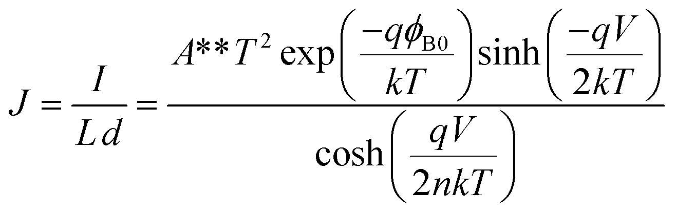 | (6) |
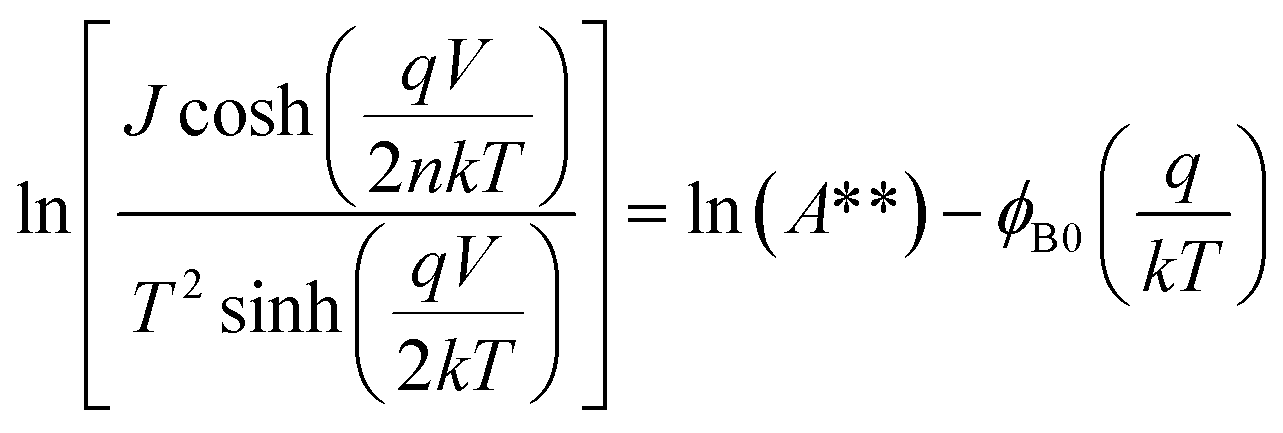 | (7) |
The above equations were fit simultaneously to obtain values for A**, ϕB0, and n. The fitting of J for different temperatures are shown in Fig. S15.† Four-point probe measurements were performed using an automatic four point probe meter (Model 280).
Conclusions
In this paper, we have clearly shown that the addition of Cu doped NiO (Cu:NiO) as a back contact layer between FTO and CuBi2O4 improves the photoelectrochemical performance of FTO/Cu:NiO/CuBi2O4 photocathodes by improving the charge carrier transport across the CuBi2O4–substrate interface. Through a series of systematic investigations of the optical and semiconductor properties of FTO, Cu:NiO, and CuBi2O4 as individual thin films and layers in the FTO/Cu:NiO/CuBi2O4 composite photoelectrode, we have provided evidence that the band positions of Cu:NiO are favourable to reduce the barrier height at the CuBi2O4–substrate interface, while simultaneously driving selective extraction of photogenerated holes (blocking of electrons). This more favourable alignment results in improved charge carrier transport across the CuBi2O4–substrate interface. As a consequence, the photocurrent density has been increased from 2.26 mA cm−2 for FTO/CuBi2O4 photocathodes to 2.83 mA cm−2 for FTO/Cu:NiO/CuBi2O4 photocathodes at 0.6 V versus RHE under backside illumination with H2O2 as an electron scavenger. This is a 25% enhancement in photocurrent density resulting in the highest absolute value reported to date for a CuBi2O4 based photocathode. These results illustrate the importance of suitable band alignment and suggest a potential improvement strategy for other oxide-based photocathode materials deposited on FTO substrates.Conflicts of interest
There are no conflicts to declare.Acknowledgements
Angang Song thanks the China Scholarship Council (File No. 201607040078) for financial support. Part of this work is supported by the German Bundesministerium für Bildung und Forschung (BMBF), project “MeOx4H2” (03SF0478A). We thank Karsten Harbauer for assistance with Cu:NiO deposition, Ulrike Bloeck for preparing TEM samples, and Marco Favaro for fruitful discussions about XPS and UPS. Fuxian Wang thanks China Postdoctoral Science Foundation (No. 2018M640784) for financial support.Notes and references
- D. Cao, N. Nasori, Z. Wang, Y. Mi, L. Wen, Y. Yang, S. Qu, Z. Wang and Y. Lei, J. Mater. Chem. A, 2016, 4, 8995–9001 RSC.
- M. K. Hossain, G. F. Samu, K. Gandha, S. Santhanagopalan, J. P. Liu, C. Janáky and K. Rajeshwar, J. Phys. Chem. C, 2017, 121, 8252–8261 CrossRef CAS.
- A. Elaziouti, N. Laouedj and A. Bekka, Environ. Sci. Pollut. Res. Int., 2016, 23, 15862–15876 CrossRef CAS.
- R. Patil, S. Kelkar, R. Naphade and S. Ogale, J. Mater. Chem. A, 2014, 2, 3661–3668 RSC.
- T. Arai, Y. Konishi, Y. Iwasaki, H. Sugihara and K. Sayama, J. Comb. Chem., 2007, 9, 574–581 CrossRef CAS.
- J. R. Bolton, S. J. Strickler and J. S. Connolly, Nature, 1985, 316, 495 CrossRef CAS.
- L. C. Seitz, Z. Chen, A. J. Forman, B. A. Pinaud, J. D. Benck and T. F. Jaramillo, ChemSusChem, 2014, 7, 1372–1385 CrossRef CAS.
- G. Sharma, Z. Zhao, P. Sarker, B. A. Nail, J. Wang, M. N. Huda and F. E. Osterloh, J. Mater. Chem. A, 2016, 4, 2936–2942 RSC.
- H. S. Park, C. Y. Lee and E. Reisner, Phys. Chem. Chem. Phys., 2014, 16, 22462–22465 RSC.
- S. P. Berglund, F. F. Abdi, P. Bogdanoff, A. Chemseddine, D. Friedrich and R. van de Krol, Chem. Mater., 2016, 28, 4231–4242 CrossRef CAS.
- N. T. Hahn, V. C. Holmberg, B. A. Korgel and C. B. Mullins, J. Phys. Chem. C, 2012, 116, 6459–6466 CrossRef CAS.
- F. Wang, A. Chemseddine, F. F. Abdi, R. van de Krol and S. P. Berglund, J. Mater. Chem. A, 2017, 5, 12838–12847 RSC.
- M. S. Prévot, X. A. Jeanbourquin, W. S. Bourée, F. Abdi, D. Friedrich, R. van de Krol, N. Guijarro, F. Le Formal and K. Sivula, Chem. Mater., 2017, 29, 4952–4962 CrossRef.
- M. S. Prévot and K. Sivula, J. Phys. Chem. C, 2013, 117, 17879–17893 CrossRef.
- A. Paracchino, J. C. Brauer, J.-E. Moser, E. Thimsen and M. Graetzel, J. Phys. Chem. C, 2012, 116, 7341–7350 CrossRef CAS.
- Y. Nakato, S. Tonomura and H. Tsubomura, Ber. Bunsenges. Phys. Chem, 1976, 80, 1289–1293 CrossRef CAS.
- F. F. Abdi and S. P. Berglund, J. Phys. D: Appl. Phys., 2017, 50, 193002 CrossRef.
- D. Kang, J. C. Hill, Y. Park and K.-S. Choi, Chem. Mater., 2016, 28, 4331–4340 CrossRef CAS.
- F. Wang, W. Septina, A. Chemseddine, F. F. Abdi, D. Friedrich, P. Bogdanoff, R. van de Krol, S. D. Tilley and S. P. Berglund, J. Am. Chem. Soc., 2017, 139, 15094–15103 CrossRef CAS.
- M. G. Helander, M. T. Greiner, Z. B. Wang, W. M. Tang and Z. H. Lu, J. Vac. Sci. Technol., A, 2011, 29, 011019 CrossRef.
- D. Cahen, G. Hodes, M. Grätzel, J. F. Guillemoles and I. Riess, J. Phys. Chem. B, 2000, 104, 2053–2059 CrossRef CAS.
- T. Minami, T. Miyata and T. Yamamoto, Surf. Coat. Technol., 1998, 108–109, 583–587 CrossRef CAS.
- E. H. Rhoderick, IEE Rev., 1982, 129, 1–14 CAS.
- S. M. Sze and K. K. Ng, Physics of Semiconductor Devices A, John Wiley & Sons, Inc., Publication, 2007 Search PubMed.
- P. Chatchai, Y. Murakami, S. y. Kishioka, A. Y. Nosaka and Y. Nosaka, Electrochem. Solid-State Lett., 2008, 11, H160 CrossRef CAS.
- M.-K. Son, L. Steier, M. Schreier, M. T. Mayer, J. Luo and M. Grätzel, Energy Environ. Sci., 2017, 10, 912–918 RSC.
- Y. Liang, T. Tsubota, L. P. A. Mooij and R. van de Krol, J. Phys. Chem. C, 2011, 115, 17594–17598 CrossRef CAS.
- I. M. Chan, T.-Y. Hsu and F. C. Hong, Appl. Phys. Lett., 2002, 81, 1899–1901 CrossRef CAS.
- M. T. Greiner, M. G. Helander, Z.-B. Wang, W.-M. Tang and Z.-H. Lu, J. Phys. Chem. C, 2010, 114, 19777–19781 CrossRef CAS.
- K. X. Steirer, J. P. Chesin, N. E. Widjonarko, J. J. Berry, A. Miedaner, D. S. Ginley and D. C. Olson, Org. Electron., 2010, 11, 1414–1418 CrossRef CAS.
- W. Septina, R. R. Prabhakar, R. Wick, T. Moehl and S. D. Tilley, Chem. Mater., 2017, 29, 1735–1743 CrossRef CAS.
- H. Peelaers, E. Kioupakis and C. G. Van de Walle, Appl. Phys. Lett., 2012, 100, 011914 CrossRef.
- T. J. Coutts, D. L. Young and X. Li, MRS Bull., 2011, 25, 58–65 CrossRef.
- S. C. Dixon, D. O. Scanlon, C. J. Carmalt and I. P. Parkin, J. Mater. Chem. C, 2016, 4, 6946–6961 RSC.
- G. A. Sawatzky and J. W. Allen, Phys. Rev. Lett., 1984, 53, 2339–2342 CrossRef CAS.
- S. P. Berglund, S. Hoang, R. L. Minter, R. R. Fullon and C. B. Mullins, J. Phys. Chem. C, 2013, 117, 25248–25258 CrossRef CAS.
- A. E. Rakhshani, Solid-State Electron., 1986, 29, 7–17 CrossRef CAS.
- L. Wei, C. Shifu, Z. Sujuan, Z. Wei, Z. Huaye and Y. Xiaoling, J. Nanopart. Res., 2009, 12, 1355–1366 CrossRef.
- J. Zhang and Y. Jiang, J. Mater. Sci.: Mater. Electron., 2015, 26, 4308–4312 CrossRef CAS.
- X.-L. Tang, H.-W. Zhang, H. Su and Z.-Y. Zhong, Phys. E, 2006, 31, 103–106 CrossRef.
- T. Nagano, M. Tsutsui, R. Nouchi, N. Kawasaki, Y. Ohta, Y. Kubozono, N. Takahashi and A. Fujiwara, J. Phys. Chem. C, 2007, 111, 7211–7217 CrossRef CAS.
- D. S. Ginley, J. Electrochem. Soc., 1978, 125, 228–232 CrossRef.
- R. Memming, Semiconductor Electrochemistry, Wiley-VCH, Boschstr., 12, 69469 Weinheim, Germany, 2000 Search PubMed.
- M. S. Prévot, Y. Li, N. Guijarro and K. Sivula, J. Mater. Chem. A, 2016, 4, 3018–3026 RSC.
- M. D. Irwin, D. B. Buchholz, A. W. Hains, R. P. H. Chang and T. J. Marks, Proc. Natl. Acad. Sci. U. S. A., 2008, 105, 2783–2787 CrossRef CAS.
- S.-H. Han, D.-Y. Lee, S.-J. Lee, C.-Y. Cho, M.-K. Kwon, S. P. Lee, D. Y. Noh, D.-J. Kim, Y. C. Kim and S.-J. Park, Appl. Phys. Lett., 2009, 94, 231123 CrossRef.
- K.-C. Wang, P.-S. Shen, M.-H. Li, S. Chen, M.-W. Lin, P. Chen and T.-F. Guo, ACS Appl. Mater. Interfaces, 2014, 6, 11851–11858 CrossRef CAS.
- Y. Ma, S. R. Pendlebury, A. Reynal, F. Le Formal and J. R. Durrant, Chem. Sci., 2014, 5, 2964–2973 RSC.
Footnote |
| † Electronic supplementary information (ESI) available: Photoelectrochemical measurements, Mott–Schottky analysis, UV-vis spectroscopy, atomic force microscopy, scanning electron microscopy, energy-dispersive X-ray spectroscopy, ultraviolet photoelectron spectroscopy, current density vs. voltage measurements, and derivations. See DOI: 10.1039/c9ta01489f |
| This journal is © The Royal Society of Chemistry 2019 |