
The versatility of copper tin sulfide
A. C.
Lokhande
 ab,
P. T.
Babar
a,
V. C.
Karade
a,
M. G.
Gang
a,
V. C.
Lokhande
c,
C. D.
Lokhande
d and
Jin Hyeok
Kim
*a
ab,
P. T.
Babar
a,
V. C.
Karade
a,
M. G.
Gang
a,
V. C.
Lokhande
c,
C. D.
Lokhande
d and
Jin Hyeok
Kim
*a
aOptoelectronic Convergence Research Center, Department of Materials Science and Engineering, Chonnam National University, Gwangju 500-757, South Korea. E-mail: abhi4502@gmail.com; jinhyeok@chonnam.ac.kr
bDepartment of Physics, Khalifa University of Science and Technology (KUST), Abu Dhabi, United Arab Emirates (UAE)
cDepartment of Electronics and Computer Engineering, Chonnam National University, Gwangju, 500-757, South Korea
dCentre for Interdisciplinary Research, D. Y. Patil Education Society (Deemed to be University), Kolhapur 416004, MS, India
First published on 18th April 2019
Abstract
In recent years, copper tin sulfide (CTS) chalcogenide compounds have witnessed applicability in various fields, rendering them as a formidable candidate for various applications. The intrinsic tunable properties accompanied by low cost, easy processing methods and eco-friendly character of CTS compounds collectively contribute to new avenues in industrial applications. In the past decade, chalcogenide CTS compounds have been extensively studied for thin film solar cell (TFSC) applications. However, with the consistent developments in scientific technology, various other applications related to optical, electrochemical, biological, functional coating and gas sensing technology have emerged. It is of vital importance to understand the driving mechanism of these applications for designing a new course for future research. Hence, in this review, the current status of various applications of CTS compounds is discussed. The key factors influencing the multifunctionality such as material properties, synthesis methods, and the doping strategy have been scrutinized. A comprehensive critical assessment of every application with ongoing developments, functional device fabrication, working mechanisms, associated issues/solutions and its potential future is made. The aim of the article is not only to overview the multiple existing applications of CTS compounds but also to develop a meritorious platform for further development in generating state of the art applications.
 A. C. Lokhande | Abhishek Lokhande is currently working as a Postdoc Fellow at Khalifa University of Science and Technology (KUST), Abu Dhabi, United Arab Emirates (UAE). He obtained his PhD degree in Materials Science and Engineering in 2019 from Chonnam National University, South Korea under the supervision of Prof. Jin Hyeok Kim. Before that, he obtained his Bachelor's (2012) and Master's degree (2014) in Mechanical Engineering from Shivaji University, India. His research interests include synthesis, characterization and development of novel efficient metal chalcogenide nanomaterials/thin films for thin film solar cells, gas sensors and energy storage/energy conversion systems. |
 P.T. Babar | Pravin Babar is currently a PhD candidate in the research group of Prof. Jin Hyeok Kim in the Department of Materials Science and Engineering at Chonnam National University. His major research interests are electrochemical energy storage and energy conversion. |
 V. C. Karade | Vijay Chandrakant Karade is presently working as a PhD scholar in the Department of Materials Science and Engineering at Chonnam National University, South Korea under the supervision of Prof. Jin. Hyeok Kim. His research interests mainly focus on the development of low cost and earth-abundant material (Cu2ZnSn(S,Se)4) based thin film solar cells. |
 V. C. Lokhande | Vaibhav Lokhande is currently a PhD candidate at the Department of Electronics and Computer Engineering at Chonnam National University, Gwangju, Republic of Korea. His research interests focus on development of semiconductors (metal oxides) for energy storage and sensing applications. |
 C. D. Lokhande | Prof. C. D. Lokhande is currently working as a Professor, Dean and Research Director in D. Y. Patil University, Kolhapur, India. Before that, he worked as a Professor in the Department of Physics, Shivaji University, Kolhapur, India (M.S.). Prof. C. D. Lokhande received his PhD in 1984. He was the recipient of the prestigious Alexander Von Humboldt Fellowship (Germany) and Brain Pool Fellowship (South Korea). He is a fellow of the Institute of Physics. He has been continuously engaged in the research field more than 30 years and has published more than 650 research articles. His research interests include the synthesis of thin films metal chalcogenides, metal oxides, conducting polymers and ferrites by chemical, physical and electrochemical methods and their applications in dye sensitized solar cells, gas sensors, energy storage devices, etc. |
 Jin Hyeok Kim | Prof. Jin. Hyeok Kim is currently working as a full professor in the Department of Materials Science and Engineering at Chonnam National University, South Korea. He received his PhD degree from the Korea Advanced Institute of Science and Technology in 1996. He was the recipient of the prestigious JSPS fellowship (Japan). He has been continuously engaged in the research field for more than 20 years and has published more than 300 research articles. He was a visiting professor at the University of California, Santa Barbara. His current research interests include the fabrication and characterization of chalcogenide based thin film solar cells especially Cu2ZnSn(S,Se)4 thin films with a focus on low-cost and earth-abundant materials using vacuum deposition techniques. In addition his research includes exploring novel cost effective materials for energy storage and conversion systems. |
1. Introduction
The search for a novel, non-toxic and cost-effective material for various applications has progressed by leaps and bounds. A ‘multifunctional material’ is a material with versatile functional capabilities and properties that could be suitably applied in a system due to its tailored intrinsic properties.1,2 The electrical, optical, structural, microstructural and compositional intrinsic properties work synergistically for realizing the multifunctionality of the material.3,4 Thus, these properties, responsible for the origin of the multifunctionality, should be considered at the forefront of designing the material for desired applications. The intrinsic material properties can be altered as per the desired need. However, screening the exact material properties for the application is necessary. Hence, a detailed understanding of the material properties and related applications is vital for achieving the desired motive. Multiple strategies such as elemental doping and materials synthesis parameters have been validated and opted to tailor the intrinsic properties.5 The first strategy deals with the doping element in the parent materials to accomplish the intended objective. This strategy is quite complicated as it requires precise control of doping elements or it may have a deteriorating effect on the material properties and its application.6 On the other hand, the latter aspect of varying the materials synthesis parameters is quite simple and easy to adopt as it provides stupendous flexibility in designing the properties for applications.7 Thus, based on the specific requirement, the suitable strategy can be adopted; however, both aspects are equally important regarding their versatility and should be widely considered for in-depth analysis. Multifunctional materials have garnered great attention due to their intriguing properties and diverse applications. The prime advantage of these materials lies in the fact that they can be employed for higher production scalability at a lower cost.8 Moreover, the multifunctional applications of these materials integrate interdisciplinary research fields that open up a wider scope and deepen our understanding of innovation.9,10 Thus, the unparalleled performance and capacity of these multifunctional materials have attracted significant attention in the scientific community.Various materials such as ZnO,11,12 TiO2,12–14 graphene oxide (GO),15,16 carbon nanotubes (CNTs)17,18 and Ag nanoparticles19–21 are being researched for multifunctional applications. Furthermore, these materials have demonstrated successful application in multiple fields including photovoltaics,22,23 gas sensing,24,25 electronics,26,27 biological28,29 and energy storage and conversion systems.30,31 Hence, the potential of these materials is immense, widely recognized and prompted the search for other materials for various applications. In the light of recent years, the ternary Cu2SnS3 (CTS) compound has displayed similar multifunctional properties and thus emerged as a potential material of research interest.32 CTS is a ternary compound from the I–IV–VI chalcogenide category and exhibits a p-type semiconductivity with a high absorption coefficient (105 cm−1) and a tunable optical band gap in the range of 0.9–1.77 eV.33,34 Thus, these unique optical properties render CTS compounds a highly suitable material for photovoltaic applications. The potential of CTS as an absorber compound in thin film solar cells was first demonstrated in 1987 by Kuku and Fakolujo,35 where a solar cell device with 0.11% power conversion efficiency (PCE) was reported. Following this report, extensive work has been conducted, and the highest conversion efficiency of 6.7% by Ge doping is achieved currently.36 As per reports, the theoretical power conversion efficiency of CTS as per the Shockley–Queisser limit is 30%.37 Hence, scope exists for further study to enhance the device performance. Currently, about 80% of the solar industry market is dominated by silicon (Si) solar cells which have a record PCE of 25%.38,39 However, the associated higher production costs of Si solar cells is a limiting factor which needs urgent attention.40 Moreover, solar cells based on CuInGaSe2 (CIGS) and CdTe compounds, irrespective of their PCEs of over 22%, suffer from the drawbacks of higher elemental cost (Ga and In) and toxic nature (Cd).41,42 Hence, CTS can be considered as an alternative material as it is composed of non-toxic, cost-effective and earth-abundant materials. Thus, CTS compounds have great potential to dominate the thin film solar cell technology market in the near future.
The application of CTS is not restricted to thin film solar cell technology despite it being a photoactive material.36,43–55 Notably, the optimum optical properties such as a high absorbance coefficient and tunable bandgap have enabled it to demonstrate effective performance in photocatalysis,56–66 photodetectors67–72 and dye-sensitized solar cells (DSSCs).73–77 These applications are exclusively driven by the optical, electrical and microstructural properties of the CTS material. The synthesis techniques play a vital role in the application part as it directly governs the electrical and microstructural properties of the material. For instance, chemical techniques such as solvothermal, chemical bath deposition (CBD), spin coating and electrodeposition are highly preferred for these optical applications as these techniques can produce porous, multi-dimensional and nanosized films with the high surface area.56,57,59–64,73–77 The films, with high surface area, can effectively generate higher electron–hole pairs and thus, higher device performance can be realized. In some cases, for efficient charge separation and conductivity improvement, reduced graphene oxide (RGO) is used along with CTS as a composite material for efficiency enhancement.61 Hence, the flexibility in fine-tuning the properties as per the desired requirements can render the material suitable for multifunctional applications. Photocatalysis is an interesting application associated with the toxic industrial dye degradation and water splitting for hydrogen energy generation. Recently, many reports have successfully demonstrated photocatalytic dye degradation (methylene blue, rhodamine, and phenol) and clean energy hydrogen generation using CTS compounds. Additionally, CTS compounds have also been applied to visible and infrared photodetection which has diverse applications in medical diagnostics, environmental monitoring, remote sensing, display technologies, etc.71–73 DSSCs have a high potential in the photovoltaic technology due to their low cost, easy fabrication techniques and higher power conversion efficiencies.71–75 Typically, the counter electrode in the DSSC plays an important role in catalyzing the redox electrolyte by the electron-transfer mechanism.78–80 Conventional DSSCs employ costly materials such as Pt and Au as the counter electrodes.81–84 Replacing these materials with inorganic semiconductors can effectively reduce the cost and help to exploit its commercial potential. Compared to primitive dyes, the employed semiconductor materials have the peculiar advantage of high extinction coefficients and large dipole intrinsic movement.85 Moreover, the semiconductors in quantum dots or nanosized form can influence the light absorption ability to contribute to achieving an enhanced power conversion efficiency. In recent years, reports based on employing CTS as a counter electrode in DSSCs have emerged. Through detailed understanding and optimization, the CTS based DSSC efficiency has increased from 4.06% to 10.18%, indicating the potential of the material for further research.73,77 Thus, CTS compounds have attracted attention as a material of potential research interest for multifunctional applications.
Besides the above applications, CTS has been actively used as an electrode material in electrochemical systems (Li-ion batteries, supercapacitors and electrochemical water-splitting). The superior electrochemical stability for larger volume expansion and higher charge storage capacity offered by CTS electrodes has opened up new avenues in battery technology.86–94 Various exciting studies based on the influence of the synthesis technique, morphology and composite materials on the battery performance and its working mechanism were reported. Although battery research using CTS electrodes is in the primordial stage, an initial discharge capacity as high as 1514.6 mA h g−1 was obtained.91 Such an outstanding performance of CTS electrodes has reflected their potential capability for battery applications. Similarly, CTS has also displayed its potential in supercapacitor application. A solvothermally synthesized CTS electrode exhibited a specific capacitance of 406 F g−1 with an energy density of 85.6 W h kg−1 and a power density of 720 W kg−1,95 while an enhanced capacitance of 704 F g−1 with an energy density of 27.77 W h kg−1 and a power density of 7.14 W kg−1 was obtained for a successive ionic layer adsorption and reaction (SILAR) technique deposited Cu rich CTS thin film electrode.96 Currently, the generation of clean energy for domestic and commercial utilization is a paramount need to mitigate existing environmental problems.97 Hydrogen generation through electrochemical water-splitting can be an effective route in the near future to cope up with energy problems.98 The oxygen evolution reaction (OER) and hydrogen evolution reaction (HER) are the two processes associated with electrochemical water-splitting.99–102 Recently, a report on a solvothermally synthesized layered structured CTS electrode demonstrated good HER performance with an overpotential of 330 mV,103 while an improved HER performance of 230 mV (ref. 104) at 10 mA cm−2 was obtained for a uniform flower-like microsphere CTS electrode. The OER activity of the CTS electrode is still unknown. However, additional extensive studies can reveal its OER activity and possibly provide scope for bifunctional water-splitting as well.
The multifunctionality of CTS compounds is not limited to optical and electrochemical applications only. Recent studies have validated the use of CTS compounds in room temperature liquefied petroleum (LPG) and H2S gas sensing.105,106 The LPG gas sensor based on a CTS/CdS heterojunction displayed an impressive performance of 56% gas response with 95% stability retention for 60 days. Additionally, the plausible gas sensing mechanism was discussed in the study to shed light on understanding the underlying material chemistry.95 Studies have also demonstrated the smart window coating (hydrophobic and hydrophilic coating)107 and antibacterial application of CTS compounds against Gram-positive and Gram-negative bacterial strains.108 Thus, the diverse applications of CTS compounds have drawn enormous attention and prompted to conduct extensive research work. Hence, we aim to review the multifunctional applications of CTS compounds and their potential future. The key factors influencing the multifunctionality from the viewpoint of material properties, synthesis techniques, and the doping strategy are discussed in detail. Furthermore, functional device fabrications with the working mechanism and associated issues/solutions are elaborated.
2. Overview of CTS compounds
Being a p-type semiconductor, the majority charge carriers in CTS are holes. The electronic structure is composed of Cu 3d and S 3p components for the valence band maximum (VBM) and Sn 5s and S 3p components for the conduction band minimum (CBM). The origin of the p-type conductivity is from the defect formed from vacancies (acceptors (VCu)) and cation–cation disorder (copper at tin anti-sites (CuSn)). The different possible defect formation mechanisms in CTS compounds are depicted in Fig. 1.109–114 | ||
| Fig. 1 The different possible defect formation mechanisms in Cu2SnSe3 (the notation of the donor/acceptor is assigned based on the defect chemistry of CZTS and CIGSe). Analogous to the above mechanisms, the formation of different defects can be extended to Cu2SnS3 by replacing the selenium with sulfur. [Redrawn from ref. 32.] | ||
The properties of the CTS compound are influenced by factors such as secondary phases, doping elements, grain size, compositional ratio and crystal structures.42 In particular, the prominent secondary phases such as CuS, Cu2S, SnS and SnS2 act as defects and influence the electronic conductivity and the optical band gap of the CTS compound42,115,116 Recently, elemental doping has proved to be a useful strategy for tailoring material properties.42 Doping produces additional energy level states in the compound and reduces recombination by promoting efficient charge generation and separation.117 Moreover, electrical properties such as carrier concentration, mobility, defect passivation and conductivity are also influenced by doping. Dopant elements such as Ge have been used for bandgap engineering in CTS compounds.47 Ge doping in CTS compounds widens the optical band gap by shifting the conduction band to a higher-level state from the Fermi-level.47 Additionally, Ge doping in CTS compounds promotes liquid assisted growth which results in a smooth, compact and large grain sized morphology, highly suitable for solar cell applications.6,118,119 Likewise, Na doping in CTS compounds influenced the electrical (enhanced carrier concentration) and morphological properties.42,45,51 Reports also showed the dependence of the optical bandgap on the grain size of CTS compounds.32,120
The Cu/Sn elemental ratio influences CTS structure formation. The Cu rich composition can form CuS, Cu2S, Cu3SnS4 and Cu4SnS4 phases, while the Cu poor composition can promote SnS, SnS2, and Cu4Sn7S16 phase formation. As seen in Fig. 2, the chemical potential phase space of CTS is quite wide.121 However, the fluctuations in the compositional Cu/Sn ratios can result in the formation of secondary phases. The Cu rich phases impart higher electrical conductivity, while the Cu poor phases affect the optical quality (optical bandgap) of CTS compounds. Hence, precise elemental control is necessary to obtain a phase pure CTS compound. The crystal structures also affect the optical and electronic properties of CTS compounds. The cubic, tetragonal, monoclinic, triclinic, wurtzite and hexagonal crystal structures of CTS compounds are reported.42
 | ||
| Fig. 2 Calculated chemical potential phase space of a Cu–Sn–S system. [Reprinted with copyright permission from ref. 121.] | ||
Out of the above structures, the tetragonal and monoclinic structures are considered to be low-temperature stable phases (<750 °C), while the cubic structure is deemed to be a high-temperature metastable phase (>750 °C). Various band gap values of 0.92, 1 and 1.28 eV for the monoclinic, cubic and tetragonal structures, respectively, were reported.42,50,122–125 These varying bandgap values are due to the different geometrical arrangements of the cations and anions in the respective structures. Out of the reported CTS crystal structures, the hexagonal structure exhibits a metallic behavior due to the absence of tetrahedral sites originating from the inherent energetic instability.126 On the other hand, the different crystal structures exhibit a semiconducting nature due to the close packing of S atoms with Cu–Sn atoms at the tetrahedral sites and absence of direct S–S atom bonding.122 Furthermore, in the study conducted by Zawadzki et al.,121 it is concluded that the Cu oxidation state also plays a vital role in the electronic properties of CTS compounds. The Cu+ state imparts the semiconducting nature, while the Cu2+ imparts metallic behavior to CTS compounds. A previous theoretical study suggests that the CTS cubic phase has several deep level defects and thus it should be avoided for thin film solar cell fabrication. Comparatively, the CTS monoclinic phase has lower defects and hence should be preferred as the highest solar cell PCEs are obtained from this phase.127 Thus, the interrelation between these parameters and the properties of CTS compounds should be understood adequately.
Various physical and chemical techniques have been adopted for the synthesis of CTS compounds (Fig. 3). The prime advantages and the impact of these techniques on the compound properties have been reviewed in our previous articles.42,120 Appropriate technique selection for materials synthesis is vital as it influences the material properties and its applications. The flexibility in achieving the variation in CTS properties for application opens up new scope for further research.
 | ||
| Fig. 3 The physical and chemical techniques adopted for the synthesis of CTS compounds. | ||
3. Multifunctional applications of CTS compounds
As mentioned earlier, CTS has gained significant research interest for multifunctional applications. Various reported applications are depicted in Fig. 4. | ||
| Fig. 4 The schematics of various reported applications of CTS compounds. | ||
3.1 Photovoltaics
Currently, energy sources such as fossil fuels, coal and petroleum products are widely used for domestic and commercial activities. However, these energy sources are limited as they will be exhausted in the coming future. In addition, the consumption of these energy sources causes pollution and global warming. Hence, effective alternatives for these energy sources should be reasonably adopted to overcome the associated problems. So far, solar energy has proved to be an effective alternative as it is a clean, extensive, inexhaustible, free and renewable source of energy. A photovoltaic (PV) system uses solar energy for its operation. It employs a device (solar cell) that converts incident light into electricity. Today, the global electricity production from PV systems is nearly 1% which is expected to increase up to 50% in the next 60 years. Hence, the reliance on PV systems for energy generation has increased significantly. Recently, thin film solar cells (TFSCs) have received widespread attention because of their low cost, efficient operation and simple device structure. These thin film solar cells consist of a light absorber layer that is responsible for charge generation. Ideally, the absorber layer should be non-toxic, cost-effective, easily synthesized and exhibit optimum electrical/optical properties. The CTS compound exhibits all these properties and hence, qualifies as a good photovoltaic material.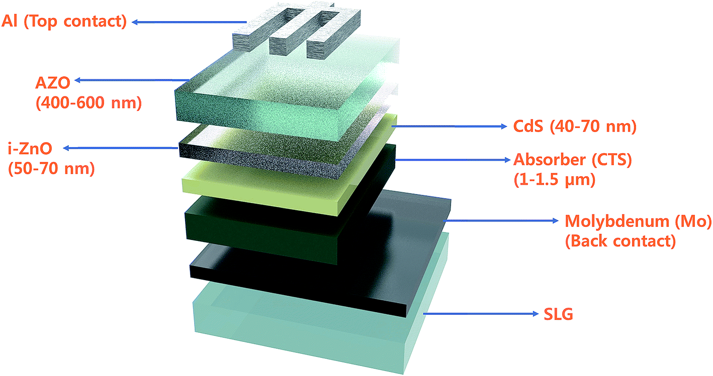 | ||
| Fig. 5 The schematics of the device architecture of the CTS TFSC. | ||
As seen, molybdenum (Mo) coated soda lime glass (SLG) is used as a supporting substrate for charge collection. Other conducting substrates such as fluorine doped tin oxide (FTO) and stainless-steel substrates are also used. In the case of fabricating flexible solar cells, polyamide substrates are employed. The active p-type absorber layer (CTS) is deposited on the Mo-SLG substrate using either physical or chemical techniques. The thickness of the absorber layer lies in the range of 1–1.5 μm for maximum visible light absorption. The deposited absorber layer is then annealed in a sulfur atmosphere (500–600 °C for 10–15 min) to obtain the desired crystallinity with optimal electrical and optical properties. The secondary phase (CuxS) formation during the sulfurization process is prominent, and hence after annealing treatment, KCN etching is performed to get rid of any such secondary phase.42 Then, two n-type semiconductors composed of a chemical bath deposited CdS buffer layer (thickness: 40–70 nm) followed by a sputter deposited intrinsic i-ZnO buffer layer (50–70 nm) are deposited. As a replacement for toxic CdS, ZnO or ZnS can be used as a buffer layer. Finally, a transparent conducting oxide (TCO) of Al-doped ZnO (AZO) is sputter deposited with metallic Al/Ag contact grids for charge collection. Ohmic contacts are made either at the top (Al) or bottom (Mo) of the solar cell. Generally, for charge collection from semiconductors, typically metal electrodes exhibiting high conductivity and high metallic work function are used (Φm > Φs). The Mo work function is approximately 5 eV, whereas commonly used Ni and Al have a work function of 5.12 and 4.28 eV, respectively.127 The exact work function values for the absorber layer is not defined, but some simulation reports consider it to be around ≤5 eV. As per semiconductor theory, the metal contact should have a high work function compared to that of the semiconducting material to form an ohmic contact.128 When the contact between a semiconductor and a metal is made, the Fermi level aligns with band bending at both conduction and valence band edges creating a favorable transport path for charge carriers.128
When light is incident on the p–n heterojunction, electron–hole pairs are generated and collected at the contacts. For efficient carrier generation and charge separation, the absorber–buffer layer interface must be smooth and intimate. Additionally, the absorber and buffer layer quality also play a decisive role in achieving an efficient power conversion efficiency of the device. Ideally, the CTS composition should be Cu poor and Sn-rich (Cu/Sn < 2). Excess Cu content can lead to shunt losses in the device.42,48 As mentioned before, plenty of reports have been published on CTS TFSC fabrication and been reviewed previously. In the present article, we will discuss some of the reports to understand the effect of influencing parameters and current status of the CTS TFSC. Despite extensive research work, the efficiency of the CTS TFSC is still low (<10%) for commercialization.
Table 1 presents the reported results of a CTS TFSC along with its preparation conditions and device fabrication structures. Both physical and chemical techniques have been employed for CTS TFSC fabrication.
| Material | Method | Study content | Annealing conditions | Band gap (eV) | Cu/Sn | Device structure | PCE (%) | Ref. |
|---|---|---|---|---|---|---|---|---|
| Cu2SnS3 | Liquid coating | General | 400 °C–2 h | 1.12 | 1.95 | SLG/ITO/n-Zno/p-CTS/graphite | 2.1 | 43 |
| Cu2SnS3 | Sputtering | Effect of Cu/Sn ratio | 580 °C–10 min (S atmosphere) | 0.89 | 1.46 | SLG/Mo/p-CTS/n-CdS/i-ZnO/AZO/Al | 2.39 | 44 |
| Cu2SnS3 | E-beam | Effect of annealing temperature | 580 °C–2 h (S atmosphere) | 0.96/1 | 1.88 | SLG/Mo/p-CTS/n-CdS/ZnO:Al/Al | 2.7 | 45 |
| Cu2SnS3 | Co-evaporation | Effect of annealing temperature | 520 °C–1 h (S atmosphere) | 0.92 | 1.84 | SLG/Mo/p-CTS/n-CdS/ZnO/ZnO:Al/Al | 3.05 | 46 |
| Cu2SnS3 | Vacuum evaporation | Na doping | 570 °C–30 min (S + Sn atmosphere) | 0.93/1.02 | 1.88 | SLG/Mo/p-CTS/n-CdS/ZnO/Ga:ZnO/Al | 4.63 | 47 |
| Cu2SnS3 | Co-sputtering | Ge doping | 550 °C–15 min (S + GeS2 atmosphere) | 1.02 | 2.33 | SLG/Mo/p-CTS/n-CdS/ZnO/Ga:ZnO/Al | 6.01 | 48 |
| Cu2SnS3 | Co-sputtering | Ge doped | 550 °C–15 min (S + GeS atmosphere) | 1.09 | — | SLG/Mo/p-CTS/n-CdS/ZnO/Ga:ZnO/Al | 6.7 | 36 |
| Cu2SnS3 | Spray-pyrolysis | K doping | 330 °C | 1.35 | — | SLG/FTO/K-CTS/n-CdS/ZnO/ZnO:Al | 0.08 | 50 |
| Cu2SnS3 | Sputtering | Ag doping | 550 °C–30 min (S + SnS atmosphere) | — | — | SLG/Mo/Ag-CTS/n-CdS/ZnO/ZnO:Al | 1 | 49 |
Tiwari et al.43 applied a direct liquid coating method (DLC) and synthesized a CTS thin film with an optical band gap of 1.12 eV having a compositional Cu/Sn ratio of 1.95. The fabricated CTS TFSC exhibited a PCE of 2.10% with a Voc of 816 mV and Jsc of 6.14 mA cm−2. The usual approach is to form a film by successive deposition of two different films followed by an annealing treatment. However, this approach results in the formation of the film with secondary phases, non-uniform morphology, and composition mismatch, eventually resulting in a reduced PCE of the device. On the other hand, the employed DLC method in the study is advantageous as it involves the use of a well-mixed precursor solution, highly suitable for the formation of a uniform and compact morphology. The obtained morphology and the fabricated device structure along with its performance parameters are shown in Fig. 6(a and b).
 | ||
| Fig. 6 (a) FESEM image of the CTS film and (b) J–V characteristics of an n-ZnO/p-CTS solar cell in the dark and under illumination (AM 1.5, 100 mA cm−2). The inset shows a schematic of a solar cell structure. [Reprinted with copyright permission from ref. 43.] | ||
As seen, the morphology of the CTS film was smooth, compact and uniform it is suitable for solar cell applications. Even though the obtained Voc (816 mV) in the study was significantly high and comparable with those of reported chalcopyrite CIGS TFSCs,129 the device performance (2.10% PCE) was low and was mostly limited by a lower Jsc (6.14 mA cm−2) and fill factor (FF = 0.42). The lower Jsc and FF were attributed to the higher series resistance (80 Ω) contributed by CTS and ITO, while the higher Voc was assigned to the diffusion of sulfur into the top layer of ZnO during the annealing treatment. The dissemination resulted in the formation of ZnS which further reacted with CTS at the interface to form a (CTS)x(ZnS)1−x compound. The optical bandgap of the formed (CTS)x(ZnS)1−x compound at the CTS/ZnO interface was higher than that of CTS, and hence it resulted in higher Voc. Furthermore, the presence of such a secondary phase at the CTS/ZnO interface could result in charge trapping leading to reduced Jsc. Even though CTS film exhibited optimum optical (1.12 eV), compositional (Cu/Sn = 1.95) and microstructural properties, the secondary phases significantly affected the performance of the device. A strategy of employing a suitable passivating layer at the interface to avoid such diffusion and secondary phase formation could enhance the efficiency.
The Cu composition also plays a vital role in influencing the PCE of the device. He et al.44 studied the influence of Cu/Sn ratio (1.46–1.61) on the PCE of the CTS TFSC. The variation in the Cu/Sn ratio was achieved by varying the Cu deposition thickness (202–234 nm) while keeping the Sn deposition thickness (313 nm) constant. The sputtered films were annealed in a sulfur atmosphere at 580 °C for 10 min to obtain the desired crystallinity. Fig. 7 presents the FESEM images of CTS films deposited at varying Cu deposition thickness. As seen from the image, CTS films deposited at lower Cu thickness (202–210 nm) exhibited a compact and void-free morphology. As the Cu deposition thickness increased (218–234 nm), the morphology transformed into a non-uniform structure with cracks and pinholes. The film deterioration became prominent with increasing Cu thickness and attributed to the formation of secondary Cu2S and Sn2S3 phases.
 | ||
| Fig. 7 The FESEM images of CTS films deposited with varied Cu thickness ranging from 202 to 234 nm. [Reprinted with copyright permission from ref. 44.] | ||
The solar cell fabricated with a lower Cu/Sn ratio (1.46) exhibited the highest PCE of 2.39% with a Voc of 208 mV and Jsc of 29.926 mA cm−2. The efficiency reduced gradually (2.39–0.82%) with increasing Cu deposition thickness (202–234 nm) (Table 2) and was mostly ascribed to the formation of a non-compact morphology. The formation of such a non-compact and cracked morphology induced substantial charge-carrier recombination which resulted in significant reduction in the Voc and hence the efficiency. Also, the formed non-compact morphology increased the resistivity (2.93 × 101 to 2.01 × 10³ ohm cm) of the films thereby affecting its charge transport system. Additionally, the increasing Cu deposition thickness resulted in increasing Cu content in the films (Cu/Sn = 1.46–1.60) resulting in higher shunt losses. Thus, the Cu/Sn ratio plays a vital role in the microstructural, electrical and compositional properties of CTS films and hence the PCE of the CTS TFSC.
| Cu thickness (nm) | V oc (mV) | J sc (mA cm−2) | FF (%) | R s (Ω cm2) | R sh (Ω cm2) | Efficiency (%) |
|---|---|---|---|---|---|---|
| 202 | 208 | 28.92 | 39.7 | 10.37 | 117.64 | 2.39 |
| 210 | 190 | 27.5 | 34.8 | 13.05 | 45.45 | 1.82 |
| 218 | 152 | 29.89 | 35.8 | 8.61 | 68.96 | 1.62 |
| 226 | 157 | 26.7 | 32.7 | 11.68 | 38.46 | 1.37 |
| 234 | 156 | 18.03 | 29.4 | 22.49 | 39.21 | 0.82 |
Besides the secondary phases and the compositional Cu/Sn ratio, the annealing temperature is also an important parameter that should be considered predominantly for TFSC fabrication. Aihara et al.45 demonstrated the influence of annealing temperature on the PCE performance of the CTS TFSC. The Cu and Sn precursors were deposited using an E-beam evaporation technique and then annealed in a N2 atmosphere with sulfur vapor at temperatures ranging from 500–580 °C. As observed from the SEM images (Fig. 8), the grain size increased with increasing annealing temperature and formation of an evident grain boundary with larger size is visible for the film annealed at/above 560 °C.
 | ||
| Fig. 8 The surface and cross-sectional SEM images of the sulfurized films at various temperatures. [Reprinted with copyright permission from ref. 45.] | ||
The solar cells fabricated with these films showed a consistent trend of increasing PCE with increasing sulfurization temperature (Table 3).
| Temperature °C | V oc (mV) | J sc (mA cm−2) | FF (%) | R s (Ω cm2) | R sh (Ω cm2) | Efficiency (%) |
|---|---|---|---|---|---|---|
| 500 | 68.1 | 8.1 | 25.5 | 7.9 | 9.2 | 0.14 |
| 520 | 69.9 | 5.7 | 25.7 | 11 | 13 | 0.1 |
| 540 | 114 | 14 | 28.6 | 6.6 | 11 | 0.44 |
| 550 | 160 | 21 | 33 | 4.6 | 15 | 1.1 |
| 560 | 244 | 28 | 37.3 | 4.4 | 24 | 2.5 |
| 580 | 244 | 29 | 38.5 | 4 | 24 | 2.7 |
Compared to other films, the film sulfurized at 580 °C showed the highest PCE of 2.7% with a Voc of 244 mV and a Jsc of 29 mA cm−2. The enhanced performance of this film was attributed to the formation of a smooth, compact, void-free, highly crystalline and large grain sized morphology which promoted efficient charge generation and separation. Additionally, the increased sulfurization temperature also facilitated more considerable carrier diffusion lengths which resulted in an improvement in the quantum efficiency at longer wavelengths (Fig. 9). However, the Cu/Sn compositional ratio was slightly increased from 1.77 to 1.89 with increasing temperature (500–580 °C) and was ascribed to the Sn loss during the sulfurization process. The elemental loss can result in the formation of spurious phases which could affect the microstructural, electrical and optical properties of the CTS compound. Several results have reported that the sulfurization time also plays a crucial role in controlling the elemental Sn loss from the absorber compound.130–132 Prolonged sulfurization leads to higher Sn loss. In this study, sulfurization was conducted for a longer time (2 h) which resulted in Sn loss. Hence, optimizing the sulfurization time can control the elemental loss for realizing an enhanced TFSC efficiency.
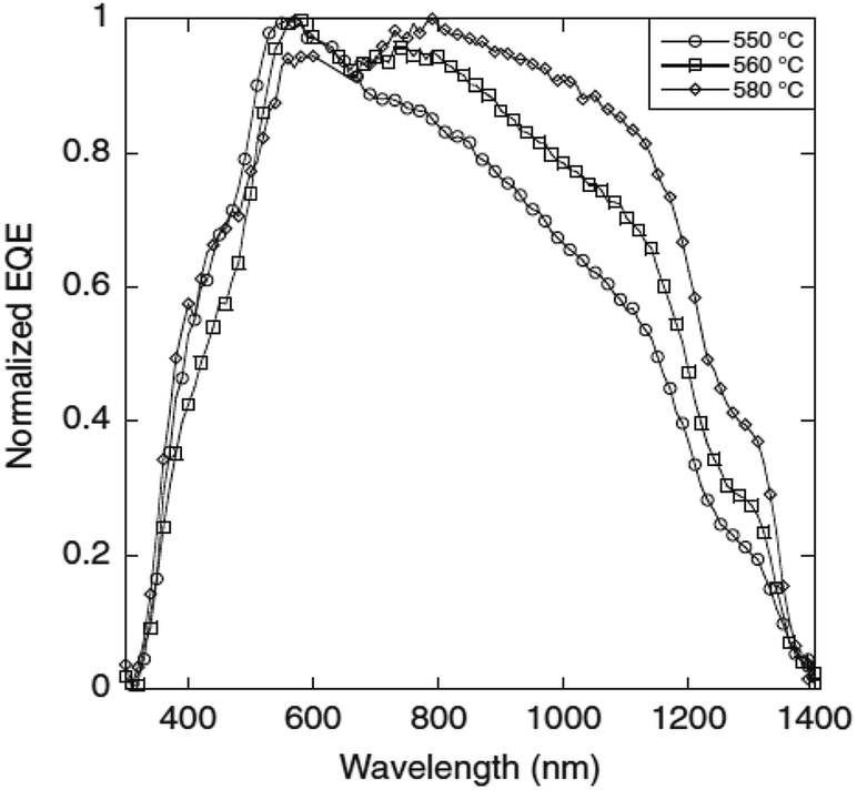 | ||
| Fig. 9 The normalized external quantum efficiency (EQE) curves of CTS solar cells fabricated at different annealing temperatures. [Reprinted with copyright permission from ref. 49.] | ||
Chierchia et al.46 also conducted a similar study of the annealing temperature effect on the PCE of TFSCs. Binary CuS and SnS precursors were sputter-deposited followed by an annealing treatment in a N2 atmosphere for 1 h. The samples were annealed at 520 and 560 °C for comparative analysis. As seen from the cross-sectional FESEM images in Fig. 10, the film annealed at 520 °C exhibits a smooth, compact and void-free morphology. However, for the film annealed at 560 °C, appreciable grain growth indicating enhanced crystallinity is observed. Moreover, the presence of a non-compact morphology with a high-density of voids and pinholes is visible. The formation of such a non-compact morphology is attributed to the elemental Sn loss from the absorber compound due to the higher sulfurization temperature (560 °C). Furthermore, the elemental loss resulted in the formation of secondary Cu3SnS4 and SnS phases in the film affecting its structural and electrical quality. The solar cell fabricated with the CTS film annealed at 520 °C exhibited a higher PCE of 3.05% as compared to the solar cell fabricated with the film annealed at 560 °C (2.37%).
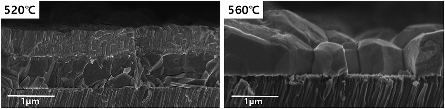 | ||
| Fig. 10 The cross-sectional FESEM images of the CTS thin films at different annealing temperatures. [Reprinted with copyright permission from ref. 46.] | ||
The solar cell fabricated with the film annealed at 560 °C exhibited higher Jsc (29.7 mA cm−2) which could be attributed to its higher grain size, while the lower Voc (219 mV) was attributed to the lower shunt resistance and larger values of Jo and n (originating from the existence of secondary phases and defect density of the film). Hence, it is evident that the annealing treatment parameters (temperature and time) affect the microstructural, optical, electrical and compositional properties and plays an important role in driving the performance of TFSCs.
Doping refers to the addition of a foreign element or impurity (electron acceptor or donors) to the parent compound to enhance its intrinsic properties. The influence of alkali metal (Na) doping on the properties of CTS thin films and their solar cell performance was assessed by Nakashima et al.47 The stacked NaF/Sn/Cu precursor was deposited on Mo/SLG glass by sequential vacuum evaporation followed by an annealing treatment in a tin and sulfur atmosphere at 570 °C for 30 min. The Cu and Sn mole ratios were fixed to 1 and 0.6, respectively, and the NaF/Cu mole ratio was varied from 0 to 1.2. Fig. 11 presents the FESEM images of CTS films prepared with the different NaF/Cu mole ratios.
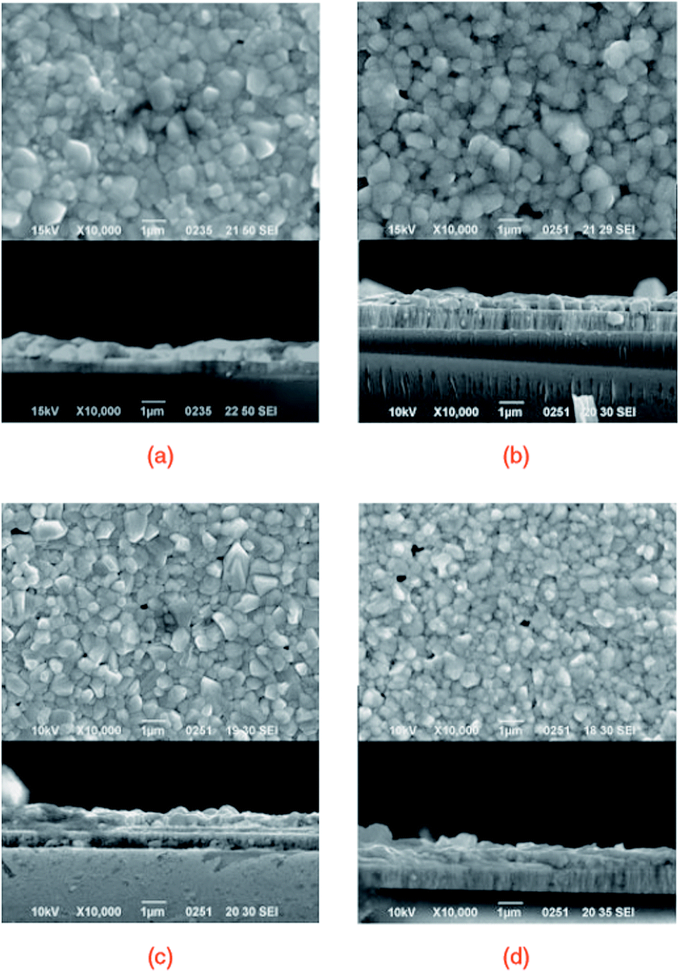 | ||
| Fig. 11 The FESEM images of the surface and cross-section of CTS thin films prepared with various NaF/Cu mole ratios: (a) 0, (b) 0.03, (c) 0.075, and (d) 0.105. [Reprinted with copyright permission from ref. 47.] | ||
As seen, the morphology is compact, and the grain size reduced with increasing NaF/Cu ratio in the precursor. A similar trend of decreased grain size with increasing Na addition was reported by Rudmann et al.133 for CIGS thin films. Moreover, the film morphology was void-free even at high temperature (570 °C) and could be assigned to the use of tin shots during the sulfurization process which compensated the Sn loss. The solar cell performance indicated a linear increase in Voc with increasing NaF/Cu ratio up to 0.075. The solar cell fabricated from a 0.075 NaF/Cu ratio displayed the highest PCE of 4.63% with a Voc of 283 mV, Jsc of 37.3 mA cm−2 and FF of 43.9%. The enhanced Voc was attributed to the increased carrier concentration by Na doping. Additionally, the Na doping lowers the thermal activation energy and pulls the Fermi level towards the valence band resulting in a potential build-up (Voc) in the structure.134 However, in the case of excess Na doping above a 0.075 NaF/Cu ratio, the performance declined (Fig. 12) and could be attributed to the generation of excess carrier concentration which resulted in reduced mobility. Hence, optimum Na doping is necessary to ensure effective performance. Previous reports have indicated that a smaller grain size is not preferable for TFSC fabrication due to the high probability of charge trapping at the grain boundaries.135,136 However, in the present study, the solar cell displayed superior performance despite exhibiting a smaller grain size. Hence, it can be concluded that electrical properties also play a key role in the performance of TFSCs.
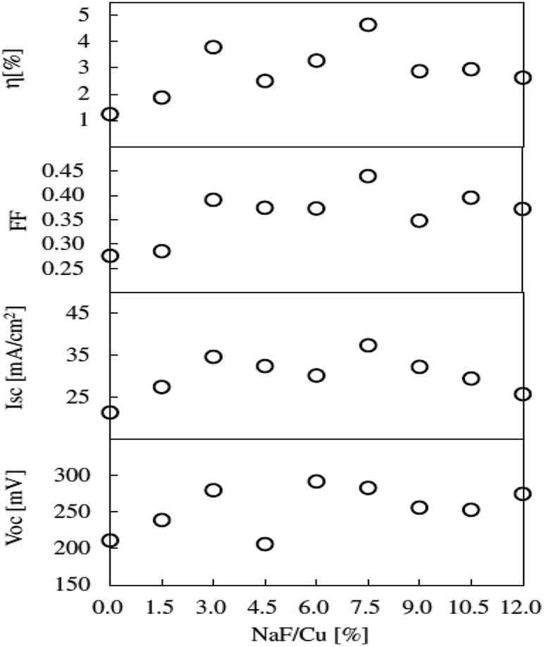 | ||
Fig. 12 The Voc, Isc, FF, and η of CTS thin-film solar cells prepared with various NaF![[double bond, length as m-dash]](https://www.rsc.org/images/entities/char_e001.gif) Cu mole ratios of the evaporating materials. [Reprinted with copyright permission from ref. 47.] Cu mole ratios of the evaporating materials. [Reprinted with copyright permission from ref. 47.] | ||
As per literature reports,137,138 the Na diffusion is influenced by the processing conditions (sulfurization temperature and time) and so stable precursors must be utilized for effective control of Na concentration. In the study conducted by Yang et al.,139 for Na doping in a Cu2ZnSnS4 (CZTS) thin film, a simple strategy was employed. An SLG substrate was placed over the as-deposited CZTS film during the annealing treatment. The Na successfully diffused into the CZTS film from the SLG substrate as well as from the bottom Mo/SLG substrate. A similar easy and cost-effective strategy can be adopted in the case of CTS TFSCs (Fig. 13).
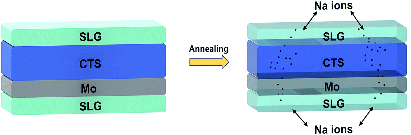 | ||
| Fig. 13 The schematic of the setup of Na doping in a CTS thin film solar cell. | ||
Other alkali metals such as Li, Rb, and K which have shown effective performance in CZTS TFSCs140 are also considered in CTS TFSCs. Li doping reduces deep defects and improves Voc,141 Rb increases the grain size and increases Voc, while K doping suppresses Sn loss and increases carrier concentration.142,143 Recently, Ruan et al.50 studied the influence of K doping in ultrasonically sprayed CTS thin films for solar cell applications.
The study results indicated the increased grain size of the CTS film with increased K concentration (Fig. 14). The improved crystallinity of the film resulted in a reduced bandgap (1.42–1.26 eV) of the film with the increased K concentration (0–3%). This bandgap narrowing effect of the CTS film was ascribed to K substitution at Cu vacancy sites which diminished the impact of the band tail state responsible for bandgap widening. The K doped CTS solar cells showed an improved efficiency from 0.03 to 0.08% with an increased K concentration from 0–2%, which was mostly attributed to the increased Jsc and Voc originating from the increased carrier concentration and increased grain size of the CTS film. At higher K doping concentration (3%), the reduced efficiency (0.03%) was ascribed to the introduced deep minority trap resulting in increased carrier recombination. A similar detrimental effect of excess K doping was observed by Tong et al.142 Thus, like Na doping, the optimized K doping concentration improved the performance of the CTS solar cell while excess doping exerted deleterious effects on the solar cell performance.
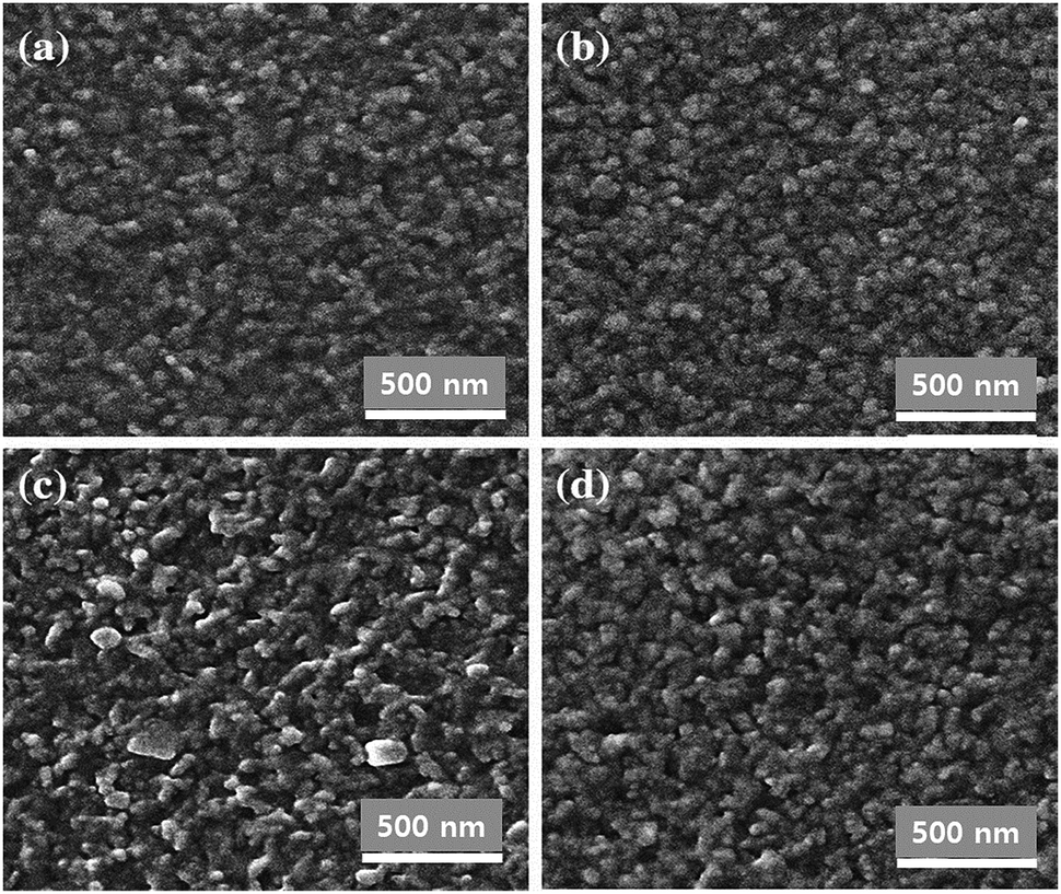 | ||
| Fig. 14 The SEM images of an (a) undoped CTS thin film, (b) 1 at% potassium doped CTS thin film, (c) 2 at% potassium doped CTS thin film, and (d) 3 at% potassium doped CTS thin film. [Reprinted with copyright permission from ref. 50.] | ||
Umehara et al.48 studied the effect of Ge doping on CTS thin films. The Cu–Sn precursors were co-sputtered and annealed in a S and GeS2 atmosphere for 550 °C for 15 min. Fig. 15(a and b) show the cross-sectional FESEM images of the undoped CTS and the Ge doped CTS film, respectively. As seen from the image, the grain size of the Ge doped CTS film was significantly larger than that of the undoped CTS film and it exhibits a dense and compact morphology. Additionally, the lateral grain size was close to the film thickness which is highly desirable for TFSCs. The formation of such a compact and large grain sized morphology was attributed to the Ge induced liquid-phase assisted growth which favors high-density atomic transport and crystallization. Similar effects of grain growth have also been observed in Ge doped CZTSSe thin films.41,144 As the size of the Ge atoms is smaller than Sn atoms, Ge displaces Sn atoms and gets easily incorporated into the CTS structure. The optical bandgap increased from 0.93 to 1.02 eV by Ge doping which is optimum for high-performance TFSCs. The increment in the optical bandgap energy by Ge doping is due to the increased repulsion of Ge–S bonding than the Sn–S bonding which shifts the conduction band to a higher-level state from the Fermi level.41
 | ||
| Fig. 15 The cross-sectional FESEM images of a (a) Cu2SnS3 film, (b) Ge doped Cu2SnS3 film on a Mo/SLG substrate and (c) the corresponding J–V characteristics of the solar cells fabricated from the undoped and Ge doped CTS films. [Reprinted with copyright permission from ref. 48.] | ||
Fig. 15(c) shows the J–V curves of the undoped and the Ge doped CTS TFSC. Compared to the undoped CTS TFSC (2.13% PCE, Voc 243 mV and Jsc 24.9 mA cm−2) the Ge doped CTS TFSC exhibited an improved performance of 6.01% PCE with a Voc of 355 mV and Jsc of 30.5 mA cm−2. The Voc is improved due to bandgap widening effect, while the Jsc and FF improved due to larger carrier diffusion length resulting from the increased grain size. Moreover, the smooth and compact morphology further reduced grain boundary density (recombination losses) contributing to overall improved performance. The bandgap depends upon the quantity of Ge doped, and thus, close control of Ge content doped is necessary as it affects the TFSC performance. Previous reports have indicated that as the Ge/(Sn + Ge) compositional ratio increases from 0 to 1, the bandgap also increases from 0.9 to 1.65 eV.36,41,144 In the present study, the Ge/(Sn + Ge) ratio was 0.17 with an optical bandgap of 1.02 eV. Thus, the flexibility in tuning the bandgap of the CTS thin film by Ge doping opens a new door in ‘Bandgap Engineering’.
One of the breakthrough technologies through which the CIGS TFSC achieved a higher PCE (22.3%) is the ‘bandgap grading’ technology.145–147 The bandgap graded structure improved the charge carrier collection efficiency and improved the performance of the TFSC. This bandgap gradation was realized by systematically varying the In/Ga compositional ratio of the absorber compound. Considering this approach, Umehara et al.36 opted for the bandgap gradation strategy in the Ge doped CTS TFSC and achieved a record PCE of 6.7%. The Ge doped CTS (CTGS) absorber layer was prepared by a similar method to that described in ref. 52. The Cu and Sn precursors were co-sputtered on Mo/SLG followed by annealing in a S and GeS2 atmosphere for 550 °C for 15 min. After that, the second layer of CTGS film was fabricated on the first layer under similar conditions with variation in the Ge/Sn ratio to achieve bandgap grading (Fig. 16).
 | ||
| Fig. 16 Schematic of the two-step fabrication process for graded-bandgap structured CTGS solar cells. (a) The first layer is deposited on a Mo-coated glass substrate. (b) The first layer is sulfurized. (c) The second layer is deposited. (d) The second layer is sulfurized and (e) a buffer layer, a window layer, and grid electrodes are formed. | ||
Three distinct types such as forward, flat and reverse bandgap grading were obtained. In the forward grading, the second absorber layer was made Ge poor and Sn-rich (lower Ge/Sn ratio) by adjusting the input sputtering power while keeping all other deposition parameters constant. The Ge composition gradually increased in the depth direction of the absorber compound (Fig. 17(a)). In the case of flat grading, it had the similar fabrication conditions to those of the first layer (Fig. 17(b)).
 | ||
| Fig. 17 The schematics of the composition profile in (a) forward gradient, (b) flat gradient and (c) reverse gradient CTGS absorber layers. | ||
The reverse grading was achieved by fabricating the absorber layer under exactly the opposite conditions to those of the forward grading (higher Ge/Sn ratio) (Fig. 17(c)). The solar cells were fabricated with these bandgap graded structures. Fig. 18(a) presents the J–V curves of the fabricated TFSCs.
 | ||
Fig. 18 (a) J–V characteristics of the samples under AM 1.5 illumination. The dashed line denotes the dark characteristics. (b) External Quantum Efficiency (EQE) spectra of the samples with white light bias. (c) The plot of [hν![[thin space (1/6-em)]](https://www.rsc.org/images/entities/char_2009.gif) ln(1 − EQE)]2vs. photon energy of the samples. [Reprinted with copyright permission from ref. 36.] ln(1 − EQE)]2vs. photon energy of the samples. [Reprinted with copyright permission from ref. 36.] | ||
As seen, the forward graded TFSC exhibited a record high PCE of 6.7% with Jsc of 26.6 mA cm−2, Voc of 442 mV and FF of 57.1% while the flat graded TFSC exhibited 6.14% PCE with a Jsc of 26.7 mA cm−2, Voc of 399 mV and FF of 57.8% and the reverse graded TFSC showed a lower PCE of 1.46% with a Jsc of 11 mA cm−2, Voc of 404 mV, and FF of 32.8%. The enhanced PCE of the forward graded TFSC was attributed to the obtained higher open circuit voltage (Voc). As seen from the EQE curves (Fig. 18(b)), the forward graded TFSC (sample A) exhibits a slightly higher EQE than the flat graded TFSC (sample B) indicating the higher charge collection efficiency of the absorber compound. Moreover, the lower performance of the reverse graded TFSC (sample C) was reflected in its lower charge carrier collection efficiency arising due to the presence of a Ge rich composition in the absorber compound. The Ge rich composition is suggested to form secondary phases (GeS and GeS2) leading to the shunt losses (low Jsc) in the TFSC. Additionally, as seen from the bandgap plot in Fig. 18(c), the band gap of the reverse graded sample is higher (1.29 eV) than the flat (1.06 eV) and forward graded samples (1.09 eV) which may form a ‘cliff-type’ conduction band offset (CBO) with the buffer layer. The ‘cliff-type’ CBO reduces the performance as it is believed to reduce the interface bandgap and cause interface recombination resulting in reduced activation energy than the bandgap. On the other hand, a ‘spike-type’ CBO is favored as the interface recombination is low and the activation energy is equal to the band gap. It has been reported that sulfides form a cliff-type and selenides form a spike-type structure with the CdS buffer layer.148 Hence, it is necessary to select an appropriate buffer-layer based on the applied absorber compound. Other combinations such as intrinsic zinc oxide (IZO)/CTS, zinc tin oxide (ZTO)/CTS, SnO2/CTS, and ZnO/CTS have been reported to have an ideal ‘spike-like’ structures and could be adopted widely (Fig. 19).149
 | ||
| Fig. 19 Photoelectron yield spectroscopy (PYS) spectra and energy band offsets of (a) CdS/CTS, (b) IZO/CTS, (c) ZnO/CTS, (d) SnO2/CTS, and (e) ZTO/CTS heterostructures. (f) The schematics of the band diagrams of the n-type semiconductor/p-type CTS structures. [Reprinted with copyright permission from ref. 149.] | ||
Thus, Ge doping and its associated bandgap-grading effects have provided a new outlook in realizing record high-efficiency CTS TFSCs. Another doping strategy, such as elemental Ag doping, which has proved beneficial for CZTS TFSCs150 is considered in CTS TFSCs. Recently, Wild et al.49 studied the effect of Ag doping in CTS TFSC applications. Ag doping promoted larger grain formation suitable for higher diffusion lengths and exhibited higher photoluminescence (PL) yield. However, TFSCs with a Ag-doped CTS film showed lower PCE (1%) than those with the pristine CTS film (3%) and this was attributed to the non-optimized device structure. As minimal literature is available on Ag-doping in CTS TFSCs, further detailed studies are necessary to understand its effects fully.
As discussed above, various parameters affect the performance of CTS TFSCs. Primarily, the absorber compound properties are interrelated and any small change in a single property can translate into a significant shift in the overall compound properties. Based on the above discussed reports, the following challenging factors should be considered simultaneously in achieving an efficient performance of CTS TFSCs.
1 Compositional control. The Cu/Sn compositional ratio is essential as it affects the efficiency of CTS TFSCs. The fluctuations in this compositional ratio can form secondary phases which affect the optical and electrical properties of the absorber compound. Based on the literature reports,42,48 CTS compounds must have a Cu poor Sn-rich composition (Cu/Sn < 2). Additional care must be taken that the CTS compound does not become excessively Cu poor as it may form Sn-rich secondary phases. The composition is also subjected to change due to annealing treatments. With optimum temperature, the formation of a smooth, compact and highly crystallized morphology suitable for fabrication of an efficient TFSC is promoted. As the temperature exceeds the optimum value, Sn, due to its lower melting point (231.9 °C), is evaporated in the form of SnS from the CTS compound leaving back an undesirable porous and non-compact morphology. Additionally, the Sn loss results in the formation of Cu rich secondary phases which affect the optical and electrical properties of the CTS compound. Thus, the control of elemental loss resulting from annealing treatments is necessary. One of the possible strategies to lower the elemental loss is to employ Sn powder during annealing treatments. The employed Sn powder, due to its generated partial-pressure, can suppress Sn loss from the CTS compound and restore morphological, compositional, electrical and optical properties.
2 Microstructural and optical quality. The morphology of the CTS compound should be smooth and compact. A smooth morphology helps to form intimate contact with the n-type buffer layer, while the compact morphology facilitates an efficient charge carrier transport. The grain size should be as large as possible to avoid charge recombination losses. The optical bandgap and the grain size have a direct relationship due to the quantum confinement effect. The optical bandgap should be in the range of 1–1.2 eV for efficient photon absorption. It is a well-known fact that the grain size increases with increasing annealing temperature. However, at the same time, the probability of the elemental loss and its associated problems become prominent. Hence, a thorough understanding and optimization of the annealing conditions are essential to achieve enhanced microstructural and optical quality of the CTS compound.
3 Absorber–buffer layer interface quality. The absorber–buffer layer interface quality also plays an important role in the PCE of TFSCs. The interface must have a smooth and intimate contact for efficient electron–hole pair migration. If the interface is rough and non-compact, the possibility of charge trapping is high which deteriorates the PCE of the solar cells. Additionally, based on band alignment, proper selection of n-type buffer layers should be considered.
4 Absorber–Mo/SLG substrate interface quality. During sulfurization treatment, Mo over the SLG substrate reacts with sulfur and forms an MoS2 secondary phase at the absorber–Mo/SLG substrate interface. Generally, the MoS2 layer in the thickness range of 100–150 nm is acceptable as its makes ohmic contact and introduces negligible contact resistance. However, at a higher thickness (<150 nm), the MoS2 layer introduces higher series resistance and lowers the minority carrier lifetime which reduces the efficiency of the TFSCs. As per previous reports,41,42 the MoS2 phase is influenced by annealing conditions (sulfurization temperature and time). Hence, effective control of this layer could be achieved through optimized annealing conditions.
5 Elemental doping control. Various doping elements such as Li, Na, K and Rb can be used in suitable combinations due to their diverse effects on CTS properties. Furthermore, as discussed before, the dopant concentration in the CTS compound is crucial and thus must be considered critically to avoid its detrimental effects.
In conventional DSSCs, nanoparticles of noble metals such as Ag, Au or Pt have been used as counter electrodes. Despite their excellent electrocatalytic activity, they suffer from the drawbacks of higher cost and stability concerns. Pt has a lower crustal abundance (0.0037 ppm) and a higher cost (50 US $ per gram) which hinders its commercial applicability. Moreover, Pt dissolves and decomposes into toxic PtI4 and PtI6 in an iodide electrolyte leading to stability issues.154 Hence, the search for alternate Pt-free materials for the counter electrode has intensified immensely in recent years. Various carbon-based materials such as carbon nanotubes,154,155 graphene156,157 and graphite158 have been explored as suitable materials for the counter electrode in DSSCs. Other materials like conducting polymers, sulfides, nitrides, and carbides have also been used.159–161 Amongst these inorganic materials, sulfides are considered as suitable materials for an efficient electrocatalytic activity due to their low cost, simple synthesis methods, and flexibility in structural and morphological properties.162–168 Recent reports have successfully demonstrated the use of CTS compounds as a useful counter electrode in DSSCs.73–77Fig. 20 presents the schematics of CTS based DSSCs. The FTO/TiO2/molecular dye constitutes the photoanode, while FTO/CTS constitutes the counter electrode. Generally, for high light absorption, a large surface area photoanode (TiO2) in the form of nanoparticles or nanorods is fabricated. Similarly, for efficient catalytic reduction of the redox electrolyte, the counter electrode is made effectively to provide maximum surface area. Both the anode and counter electrodes are immersed in the redox electrolyte and are separated using a thin polypropylene or surlyn spacer (60 μm). Generally, polysulfide and polyiodide redox couple electrolytes are used.
 | ||
| Fig. 20 The schematics of CTS based DSSCs with a photoanode consisting of a dye-sensitized TiO2 film, a CTS counter electrode and a redox electrolyte filled between the photoanode and counter electrode. | ||
The working mechanism of CTS based DSSCs is given as below.
(a) The incident light (hν) is absorbed by the photo-sensitizer (molecular dye), and an electron is excited from the ground state (S) to the conduction state (S*). This excited electron is transferred to the TiO2 conduction band, and hence the sensitizer is oxidized (S+). The generated electron diffuses into the back-contact electrode (FTO) and moves to the CTS counter electrode through an external circuit.
| S + hν = S* | (1) |
| S* = S+ + e− (TiO2) | (2) |
(b) The oxidized sensitizer (S+) is reduced to the ground state (S) by accepting the electrons from the I− ion redox mediator. Two I− ions are oxidized to form elementary iodine which further reacts with the I− ion to form the I3− redox mediator. The oxidized I3− redox mediator then diffuses to the counter electrode (CTS) and gets reduced to I− ions by accepting the electrons.
| S+ + e− = S | (3) |
| I3− + 2e− (CTS) = 3I− | (4) |
Various factors such as the redox potential of the mediator (I−/I3−), TiO2 Fermi level, excited and ground state of the sensitizer and the electrocatalytic activity of the counter electrode (CTS) affect the performance of the DSSCs.
Table 4 lists the experimental parameters for CTS synthesis and the type of study performed for DSSC applications. Generally, it is well known that the electrocatalytic properties are influenced by the microstructural and electrical properties of the counter electrode. One of the important strategies to maintain these properties is the proper selection of materials synthesis techniques. Generally, chemical techniques such as solvothermal or hydrothermal are preferred as these techniques have the unique capability to produce high surface area with a porous and large grain sized morphology.
| Material | Method | Phase | Band gap (eV) | Morphology | Type of study | Device | Efficiency (%) | Ref. |
|---|---|---|---|---|---|---|---|---|
| Cu2SnS3 | Solvothermal | Tetragonal | 1.15 | Microsphere (2 μm) | Comparison of CTS and Cu1.8S PCE performance | Anode: ZnO/ZnSe/CdSe | FTO/CTS: 4.06% | 73 |
| Cu1.8S | Solvothermal (250 °C–48 h) | Rhombohedral | 1.33 | Microsphere (500 nm) | Counter: FTO/CTS, FTO/Cu1.8S | FTO/Cu1.8S: 3.65% | ||
| Electrolyte: polysulfide | ||||||||
| Spacer: 60 μm polypropylene | ||||||||
| Cu2SnS3 | Solvothermal (200 °C–24 h) | Cubic | — | Porous net-like structure (600 nm thick) obtained using glycol (FA) | Effect of morphology (solvent variation) on the PCE performance (as-deposited and annealed samples (500 °C–1 h)) | Anode: TiO2 with N719 dye | As-deposited | 74 |
| Vermiculate nanorods (260 nm thick) obtained using ethanol (FB) | Counter: Mo/CTS | (FA): 2.30% | ||||||
| Microcluster (950 nm) obtained using DMF (FC) | Electrolyte: I3−/I− | (FB): 0.66% | ||||||
| Spacer: 42 μm | (FC): 1.75% annealed (500 °C–1 h) | |||||||
| (FA): 3.35% | ||||||||
| (FB): 2.56% | ||||||||
| (FC): 2.88% | ||||||||
| Cu3SnS4 | Solvothermal (200 °C–25 h) | Cubic | — | Dendritic structure (200–300 nm) | Effect of film thickness on PCE (dropcast: 0.1–0.4 ml for PCE) | Anode: FTO/CTS N719 dye | RF Pt: 7.24% | 75 |
| Counter: FTO/CTS | 0.1 ml: 6.47% | |||||||
| Electrolyte: I3−/I− | 0.2 ml: 7.13% | |||||||
| Spacer: 60 μm thermal-plastic surlyn | 0.3 ml: 5.89% | |||||||
| 0.4 ml: 5.35% | ||||||||
| Cu3SnS4 | Electrodeposition + solvothermal (200 °C–24 h) | Kuramite | — | Homogeneous and compact layer | Varied solvothermal reaction times | Anode: FTO/TiO2 | 3 h: 5.68% | 76 |
| (640 nm) composed of nanoflakes | 3, 6, 12, and 24 h and checked its effect on PCE of as deposited samples | Counter: FTO/CTS | 6 h: 6.60% | |||||
| (50–90 nm length) | Electrolyte: I3−/I− | 12 h: 7.43% | ||||||
| 24 h: 7.80% | ||||||||
| Rf Pt: 6.52% | ||||||||
| Cu2SnS3 | Spin coating (320 °C–15 min) | Tetragonal | — | Dense and continuous S/f (70 nm thick and 20–3 nm size) | Performed 3 studies | Anode: FTO/TiO2 | RF Pt: 9.24% | 77 |
| (1) Compared FTO/CTS vs. FTO/Pt by CV and EIS and found that FTO/CTS is better | Counter: FTO/CTS | CTS: 10.18% | ||||||
| Ligand free | (2) Effect of annealing temp. (320–440 °C) | Electrolyte: (I3−/I−) for PCE and (Co2+/Co3+) for study | ||||||
| (3) Varied spin coating solution concentration (0.05–0.2 M) | Spacer: surlyn (60 μm) |
The successful application of CTS compounds as a counter electrode in DSSCs was first demonstrated by Xu et al.73 In the study, a systematic comparison between the binary (Cu1.8S) and ternary (CTS) sulfide compounds was performed. The compounds were synthesized by a simple and cost-effective solvothermal method using triethylene glycol (TEG) solvent. The TEG is important as it plays multiple roles as the solvent, chelating agent and capping agent. Being a chelating and capping agent, it effectively regulates the release rate of precursor ions (Cu2+ and Sn4+ ions), prevents particle aggregation and promotes the formation of uniform and dispersed particles.
As seen from the FESEM images in Fig. 21(a and b), nearly mono-dispersed microspheres of CTS (2 μm size) and Cu1.8S (500 nm size) are obtained. The advantage of these well-dispersed particles lies in the fact that they provide a larger surface area for effective catalytic reduction of the redox electrolyte. The optical band gap was found to be 1.15 and 1.33 eV for CTS and Cu1.8S particles, respectively. The variation in the bandgap of these compounds can be attributed to the discrepancy in the particle size and structure. A DSSC was fabricated using CTS and Cu1.8S as the counter electrode. ZnO/ZnSe/CdSe was used as the photoanode, and a polysulfide redox couple was used as the electrolyte.
 | ||
| Fig. 21 The FESEM image of the synthesized (a) Cu2SnS3 (CTS) and (b) Cu1.8S particles. [Reprinted with copyright permission from ref. 73.] | ||
Fig. 22(a) shows the J–V curves of the DSSC fabricated with these electrodes. The DSSC fabricated with a CTS counter electrode exhibited a higher PCE of 4.06%, while the DSSC fabricated with Cu1.8S and FTO as the counter electrode exhibited a lower PCE of 3.65% and 0.25%, respectively. The enhanced performance of the CTS counter electrode is clear evidence of smaller interfacial recombination of the counter electrode with the electrolyte. The origin of the enhanced performance was attributed to two factors. The first is the bandgap. The smaller bandgap of CTS (1.15 eV) than Cu1.8S (1.33 eV) indicates the higher photon absorption and carrier generation in CTS than in the Cu1.8S compound. Second, as seen from Fig. 22(b), the charge transfer resistance (Rct) of CTS (6.2 Ω cm2) is lower than that of Cu1.8S (11.4 Ω cm2) indicating an efficient electron charge transport from the electrode to the electrolyte. Hence, it is quite clear that the microstructural, optical and electrical properties of CTS play an important role in influencing the performance of DSSCs.
 | ||
| Fig. 22 (a) The current density–voltage (J–V) characteristics of a solar cell using FTO, Cu1.8S/FTO and CTS/FTO counter electrodes and (b) the Nyquist plots of FTO/FTO, Cu1.8S/FTO–Cu1.8S/FTO and CTS/FTO–CTS/FTO symmetric cells in polysulfide redox electrolyte. [Reprinted with copyright permission from ref. 73.] | ||
Various experimental parameters, such as the solvents, chelating agents, reaction time and temperature, of chemical techniques are known to affect the structural and morphological properties of the synthesized compound. In a study performed by Xu et al.,74 the effect of different solvents such as ethylene glycol (EG), ethanol and N,N-dimethylformamide (DMF) on the morphology of the solvothermally synthesized CTS films was evaluated. The obtained morphologies are depicted in Fig. 23.
 | ||
| Fig. 23 The FESEM images of CTS films obtained from (a) ethylene glycol, (b) ethanol and (c) DMF solvents. [Reprinted with copyright permission from ref. 74.] | ||
As seen from the figure, significant changes in the morphology are obtained. The CTS film synthesized using EG solvent exhibits a porous net-like morphology with the pore size in the range of several hundreds of nanometers, while the films synthesized using ethanol and DMF solvents have compact vermiculate nanorods and a microcluster-like morphology, respectively. The DSSC measurement revealed that the porous net-like structure using EG solvent exhibited the highest PCE of 2.30% with a Jsc of 6.16 mA cm−2 and Voc of 690 mV. Compared to the other morphologies, the porous net-like structure provided a larger surface area of electroactive sites and hence promoted efficient catalytic reduction of the redox electrolyte. Furthermore, the same film was annealed at 500 °C for 1 h in Ar gas to understand the influence of the annealing treatment. The morphology did not change very significantly, but an increase in the PCE is noted. The PCE was improved to 3.35% with a Jsc of 6.54 mA cm−2 and a Voc of 730 mV. This improved performance was mostly ascribed to an improvement in Jsc (6.16 to 6.54 mA cm−2) originating from the enhanced photo-induced carriers of the film due to an annealing treatment as seen from the IPCE spectra Fig. 24. Thus, it is clear that the control of simple experimental parameters can easily influence the performance of the DSSC.
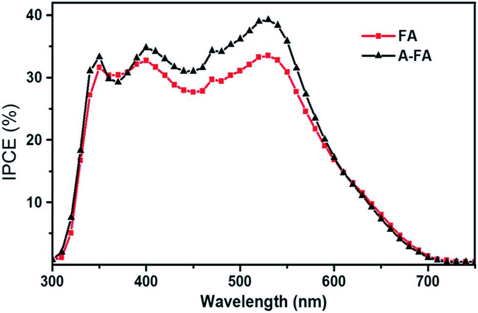 | ||
| Fig. 24 The IPCE spectra of the DSSC based on the as-deposited CTS film (FA) and annealed CTS film (A-FA). [Reprinted with copyright permission from ref. 74.] | ||
Zhao et al.75 in their study demonstrated the effect of CTS film deposition thickness on the PCE of the DSSC. The Cu rich CTS nanoparticles were synthesized using a solvothermal method and then drop cast on the FTO substrate to form the counter electrode. The thickness of the CTS film was varied using the drop casting solution concentration (0.1–0.4 ml). After coating, the CTS films were sulfurized at 550 °C for 35 min in a sulfur atmosphere to achieve crystallinity. The as-synthesized CTS nanoparticles (Fig. 25(a)) exhibit a rough and a porous dendritic morphology (200–300 nm size) which is highly suitable for providing a larger surface area for an efficient electrocatalytic activity. Fig. 25(b–e) show the cross-sectional FESEM images of CTS films deposited at various solution concentrations. The CTS film thickness increased linearly (2.1–4.8 μm) with the increased solution concentration (0.1–0.4 ml). Moreover, the film porosity due to the existence of interconnected nanocrystals and interspaces became prominent with increasing film thickness. The CTS film deposited at 2.9 μm thickness exhibited the highest PCE of 7.13% with a Jsc of 13.51 mA cm−2 and a Voc of 710 mV. Further increase in film thickness resulted in decreased PCE. The reduction in the PCE was attributed to the current density (Jsc) drop (11.21 to 10.30 mA cm−2) due to the increasing film thickness. The thicker films introduced larger series resistance in the film which adversely affects the electron charge transport mechanism between the counter electrode and the electrolyte, and hence reduced the performance of the DSSCs. However, the PCE of the CTS based DSSC (7.13%) in the study is lower than that of the reference Pt-based DSSC (7.24%).
 | ||
| Fig. 25 (a) The FESEM image of the as-synthesized CTS nanoparticles and the cross-sectional FESEM images of the CTS thin film with drop volumes of (b) 0.1, (c) 0.2, (d) 0.3, and (e) 0.4 ml. [Reprinted with copyright permission from ref. 75.] | ||
Chen et al.76 studied the effect of the solvothermal reaction time of the CTS counter electrode on the performance of the DSSCs. In the study, a novel approach of adopting the cost-effective electrodeposition and solvothermal techniques was employed. Initially, the Cu–Sn alloy precursors were electrodeposited on the FTO substrate and then subjected to a solvothermal treatment in ethanol solvent using sulfur powder. The reaction temperature was fixed at 200 °C and the reaction time was varied as 3, 6, 12 and 24 h. Fig. 26(a) shows the Raman spectra of CTS films deposited at different reaction times. As seen from the spectra, at a lower reaction time (3 h), along with the CTS peak (320 cm−1), the peaks at 283 and 315 cm−1 reflect the presence of Cu2S and SnS2 secondary phases, respectively. With further increase in reaction time to 12 h, the SnS2 peak diminished in intensity and only a peak assigned to Cu2S was observed which was attributed to the diffusion reaction of the Sn4+ ions into the Cu2S structure. Finally, at 24 h reaction time, the diffusion reaction was accomplished, and only a single peak (320 cm−1) corresponding to the formation of CTS was observed. Thus, the mechanism of phase formation of the CTS compound is influenced by the reaction time. The FESEM image (Fig. 26(b)) of the CTS film synthesized at 24 h reaction time exhibits an interconnected nanoflake-like morphology providing a larger surface area for efficient catalytic activity. Additionally, the calculated density of states (DOS) indicated the existence of metallic character in the synthesized Cu rich CTS compound suitable for an efficient charge transfer from the electrode surface to the electrolyte.
 | ||
| Fig. 26 (a) The Raman spectra of CTS films synthesized at various reaction times (3, 12 and 24 h) and (b) the FESEM image of the CTS film synthesized at 24 h reaction time. [Reprinted with copyright permission from ref. 76.] | ||
The J–V curves and the corresponding photovoltaic parameters of the fabricated DSSCs with CTS films deposited at varied reaction times are summarized in Fig. 27(a and b), respectively. As observed, the PCE increases linearly from 5.68 to 7.80% with the increased reaction time from 3 h to 24 h. The enhancement in performance was attributed to the reduction in the secondary phases in the film due to the increase in reaction time. The photovoltaic parameter (FF) also showed a similar consistent trend as the fill factor (FF) increased significantly from 55% to 66% with increasing reaction time. The FF represents the internal resistance of the solar cell which comprises contact resistance, substrate resistance, bulk electrode resistance, photoanode resistance and the charge transfer resistance between the electrode and the electrolyte. Hence, the increased FF reflects the reduced internal resistance of the solar cell due to the formation of a phase pure CTS compound.
 | ||
| Fig. 27 (a and b) The J–V curves and the corresponding photovoltaic parameters of the fabricated DSSCs with the CTS films deposited at varied reaction times. [Reprinted with copyright permission from ref. 76.] | ||
Compared to the Pt reference electrode (6.52% PCE), the CTS electrode exhibited higher efficiency (7.80% PCE) implying, a higher rate of hole recovery at the electrode–electrolyte interface. Additionally, the microstructure with the larger surface area and the metallic character of the compound collectively contributed to an improved electrocatalytic activity. Thus, it is clear that the secondary phases in the compound have a negative impact on the performance of the DSSCs and should be controlled by optimizing the experimental conditions.
One of the critical aspects that should be considered in colloidal nanoparticle synthesis is the nanoparticle surface stabilization with organic ligands. The organic ligands cap the nanoparticle surface and avoid aggregation with the surrounding particles. This results in higher particle dispersibility, which ultimately provides a larger surface area for the catalytic reduction of the redox electrolyte.169 However, on the other hand, these organic ligands exhibit insulating nature and hence restrict the electron charge transport between neighboring particles resulting in reduced electrical conductivity and, consequently, the electrocatalytic activity.166,170–172 Therefore, the synthesis of ligand-free materials is of utmost importance for realizing an efficient catalytic activity of counter electrodes in DSSCs. The primary source of origin of organic ligands is from the same solvents used in the synthesis of the compound. Thus, careful solvent selection is vital to produce ligand-free materials.
In recent years, ligand-free CZTS and CTS thin films have been utilized for an efficient photovoltaic application using the hydrazine chemical approach. However, hydrazine is highly toxic and flammable and thus considered unsuitable for mass scale utilization. As an alternative, Liu et al.77 employed a mixture of a thiol–amine solvent for the synthesis of ligand-free CTS compounds. The two-component thiol–amine solvent has a strong reducing capability and can easily dissolve binary chalcogenides to form a homogeneous complex which can be further transformed into a ternary semiconducting phase upon heating. Binary Cu2S and SnS2 powders were dissolved in a mixture (10:1) of ethylenediamine and ethanedithiol to form a homogeneous solution. The solution was spin coated on an FTO substrate and annealed at 320 °C for 15 min to form a CTS film. Fig. 28(a and b) show the surface and cross-sectional FESEM images of the CTS film on the FTO substrate.
 | ||
| Fig. 28 (a) The surface FESEM image of the CTS thin film on FTO glass and (b) the corresponding cross-section FESEM of the CTS thin film. [Reprinted with copyright permission from ref. 77.] | ||
As seen, the film is uniform, compact and non-porous having a thickness of about 70 nm. Being a compact film, the electrolyte diffusion in the film can be neglected. Hence, the derived catalytic performance would be expected from the film surface only. Fig. 29(a) depicts the J–V curve of the DSSC fabricated using the CTS film and the reference Pt counter electrode. Compared to the reference Pt counter electrode (9.24% PCE), the DSSC fabricated with the CTS counter electrode exhibited the highest PCE of 10.18%. The performance of the CTS electrode mostly improved due to the lower series resistance (Rs) and increase in Voc and Jsc values.
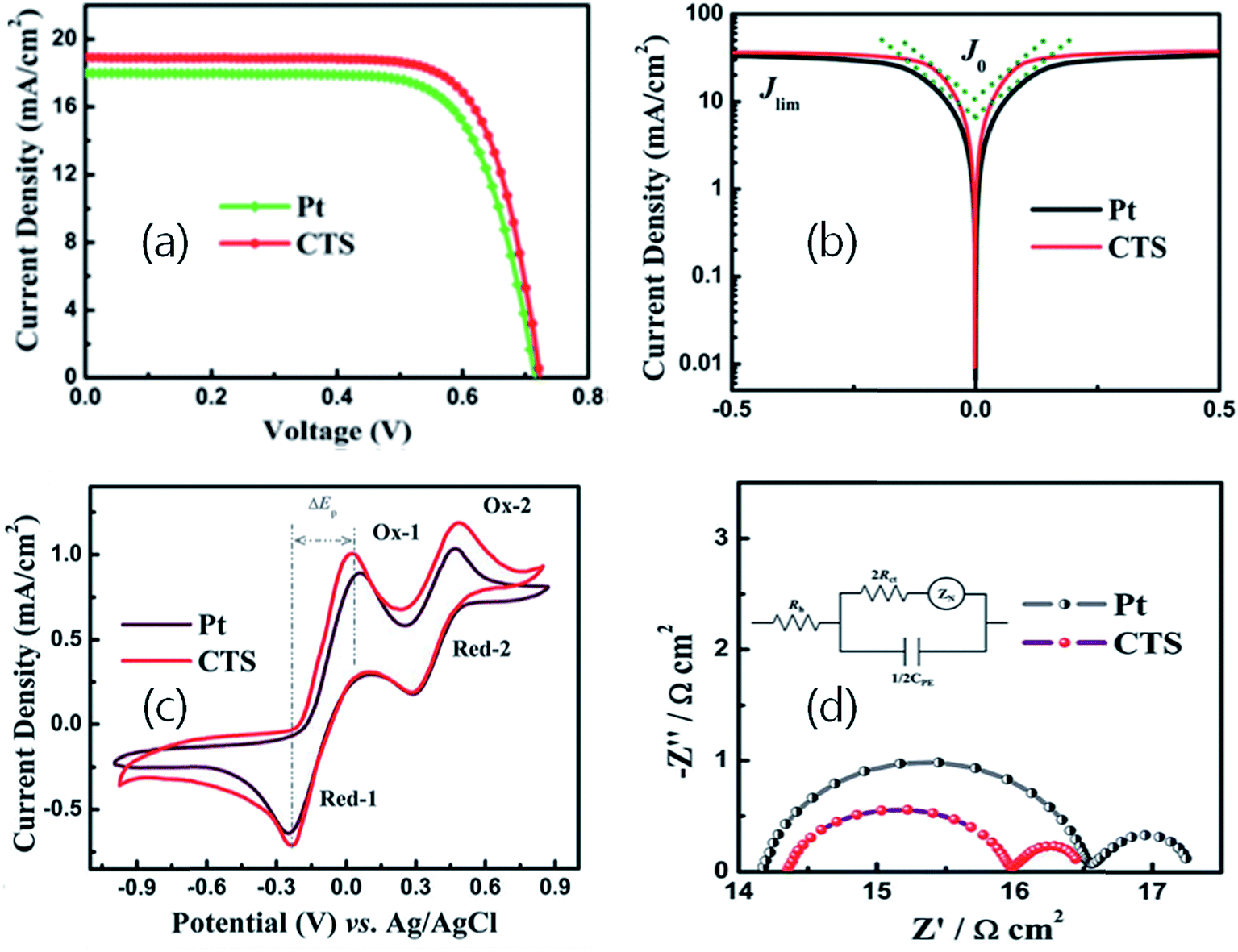 | ||
| Fig. 29 (a) Representative photocurrent–voltage curves of C101 dye-sensitized solar cells based on Pt and CTS electrodes (light intensity: 100 mW cm2, AM 1.5), (b) Tafel polarization curves of the Pt and CTS symmetrical cells, (c) cyclic voltammograms of I3−/I− redox species for the Pt and CTS electrodes. The scan rate was set to 20 mV s−1 and room temperature was 25 °C. (d) Nyquist plots from the EIS measurements of the Pt and CTS symmetrical cells. The inset shows the equivalent circuit for fitting the EIS spectra. [Reprinted with copyright permission from ref. 77.] | ||
The Tafel polarization curves depicted in Fig. 29(b) indicate the higher values of exchange current density (Jo) and higher limiting diffusion current density (Jlim) of the CTS electrode due to reduction in charge recombination. Moreover, as seen from the CV curves in Fig. 29(c), compared to the Pt electrode, the CTS electrode exhibits higher peak to peak separation (oxidation–reduction peak) and higher attainable current densities indicating an enhanced electrical conductivity and higher availability of organic ligand-free electroactive sites. Also, the Nyquist plot in Fig. 29(d) shows the lower charge transfer resistance (Rct) of the CTS electrode reflecting an improved charge carrier transport for the catalytic reduction of the redox electrolyte. Thus, the improved electrical properties in terms of enhanced conductivity and reduced charge recombination due to the formation of a ligand-free CTS compound resulted in an improved performance. As per previous reports,73–75 the morphology of the counter electrode needs to be rough and porous for providing larger electroactive sites. However, in the current study, the morphology despite being compact and non-porous demonstrated the highest PCE due to its improved electrical properties. Hence, it can be concluded that along with morphology the intrinsic electrical properties of the counter electrode are decisive contributors as well. In the study, if the ligand-free CTS film was synthesized with a porous microstructure, a further tenfold improvement can be possibly expected. The achieved efficiency of 10.18% in the study is the highest amongst those of other reported CTS based DSSCs and close to the world record efficiency of 14.7% achieved with a FTO/Au/GNP (graphene nanoplates) counter electrode.173 The following factors should be considered for overcoming the shortcomings in the performance of DSSCs.
1 Morphology. The morphology plays a vital role in the catalytic performance of the DSSCs. The rough and porous morphology of CTS is preferred as it provides the maximum surface area for the catalytic reduction of the redox electrolyte. A smooth and compact morphology tends to have reduced surface area and thus, the catalytic performance is reduced. Proper selection of materials synthesis technique can help to achieve high surface area. The chemical techniques such as CBD, electrodeposition, solvothermal and hydrothermal provide the desired porous morphology.
2 Electronic conductivity. The counter electrode in the DSSC must have high electrical conductivity for efficient electron charge transport between the electrode and electrolyte. Cu rich CTS allotropes such as Cu3SnS4 or Cu4SnS4 with high electrical conductivity should be preferred. Various carbon-based materials such as carbon nanotubes (CNTs), graphite and graphene composites can be used along with the CTS film for improvement in electrical conductivity.
3 Secondary phases. The secondary phases (CuS, Cu2S, SnS, and SnS2) in CTS compounds affect the electrical properties of the film. The secondary phases result in larger charge carrier recombination and thus, reduce the performance. Hence, the phase pure synthesis of CTS should be achieved by optimizing various experimental parameters.
4 Thickness. The counter electrode film thickness is an important factor. Generally, a higher film thickness results in lower performance due to increasing series resistance. On the other hand, a lower film thickness also results in a reduced performance due to the limited availability of active electrode catalytic sites. Hence, the trade-off between the film thickness and the catalytic performance needs to be studied for optimal performance.
5 Thermal treatment. Thermal treatment of the counter electrode can also affect the catalytic performance of the DSSCs. Thermal treatment can enhance the charge carrier transport mechanism and thus, improve the conductivity of the film for efficient catalytic activity. However, at the same time, it should also be considered that the thermal treatment increases the grain size of the CTS film which reduces the active surface area sites and thus, deteriorates the catalytic performance of the CTS film. Hence, a thorough optimization of the thermal treatment (annealing temperature and time) is necessary.
6 Organic ligand-free compound synthesis. The strategy for obtaining organic ligand-free CTS compounds should be opted. Ligand-free compound synthesis enhances the electrical conductivity. Additionally, it can accelerate the surface activity of the compound for realizing augmented electro-catalytic reduction of the redox electrolyte.
Thus, it can be concluded that CTS has great potential in photovoltaic (PV) applications. The CTS based TFSC exhibits the advantages of low cost, non-toxicity and easy processability as compared to CIGS and CdTe based TFSCs. However, the performance of the CTS based TFSCs (PCE) is quite lower than that of CIGS/CdTe based solar cells. Similarly, CTS based DSSCs are cost effective, can be easily processed and exhibit an efficient performance. CTS based DSSCs are quite reliable; however, they suffer from the serious drawback of instability due to dye decomposition. Hence, additional studies are required to understand the current drawbacks and generate solutions for the same to enhance the performance.
3.2 Photocatalysis
Photocatalysis is a process of expediting the chemical reaction in the presence of a photocatalyst. A photocatalyst consumes the incident photon energy for accelerating the reaction kinetics without itself undergoing any chemical reaction. The generated electron–hole pairs separate and migrate to the surface of the photocatalyst where they act as an active reducing and oxidizing species.174 These generated redox species form the driving force for the photocatalysis application. Organic dye degradation into simple compounds and water splitting for H2 and O2 production are the major applications of photocatalysis.The CTS compound exhibits all the essential properties demanded in the photocatalytic application. In the last couple of years, several reports56–64 have successfully demonstrated the photocatalytic activity of CTS compounds for toxic dye degradation including methylene blue (MB), rhodamine B, eosin, phenol, etc. The key factors affecting the photocatalytic efficiency of CTS compounds are their optical, microstructural and electrical properties. Fig. 30 depicts the schematic of the working mechanism of the photocatalytic activity of the CTS compound. When the light is incident on the CTS compound, electron–hole pairs are generated. The incident light excites the electron to the conduction band leaving behind holes in the valence band. The generated holes in the valence band are accepted by the hydroxyl group (OH) in the dye solution to form free hydroxyl radicals (OH˙). Simultaneously, the electrons in the conduction band reduce the surface absorbed molecular oxygen (O2) to superoxide radicals (O2−˙) and other active species (HO2˙ or OH˙). Thus, the collective contribution of these formed radical species results in the degradation of the organic dye molecule. The rate of dye degradation depends on the number of reactive radicals generated. A compound with a high optical absorption can maximize the electron–hole pair generation, while a porous microstructure (high surface area) can provide larger catalytic sites for the radical species formation. Hence, the synergistic effect of high optical absorption coupled with a porous microstructure can enhance the photocatalytic activity of the compound.
 | ||
| Fig. 30 The schematic of the working mechanism of the photocatalytic activity of the CTS compound. | ||
The reaction mechanism of dye degradation is given below
| CTS + hν = CTS (ecb− + hvb+) | (5) |
| hvb+ + OH = OH˙ (valence band) | (6) |
| ecb− + O2 = O2−˙ (conduction band) | (7) |
| OH˙ + O2−˙ + dye = degraded products | (8) |
The photocatalytic activity of the CTS compound for industrial dye degradation was first demonstrated by Tan et al.56 In the study, CTS particles with an optical bandgap of 2.42 eV were synthesized using a single step solvothermal method. Fig. 31(a) depicts the FESEM image of CTS particles. As seen, the 2D interconnected nanosheets are coupled to form a flower-like morphology. Additionally, the flower-like nanosheets aggregated to form numerous hierarchical porous structures which provide the maximum surface area for the catalytic sites. Fig. 31(b) depicts the absorption spectrum of the MB dye in the presence of CTS flowerlike particles (20 mg) under visible light irradiation. As seen from the spectrum, the characteristic absorbance peak of MB dye (663 nm) reduced linearly with increasing irradiation time. The peak completely disappeared after 4 h irradiation indicating the complete degradation of the MB dye. The entire dye degradation process (4 h) could have been accelerated further if the bandgap of the synthesized compound lay in the optimal range (1–1.5 eV) of efficient visible light absorption.
 | ||
| Fig. 31 (a) The FESEM image of an individual CTS flowerlike architecture and (b) the temporal evolution of the absorption spectra of MB in the presence of CTS flowerlike architectures under visible light irradiation. [Reprinted with copyright permission from ref. 56.] | ||
In the study conducted by Maheskumar et al.,57,58 a systematic comparison of the ball milled, and the solvothermally synthesized Cu rich CTS particles for catalytic dye degradation was performed. As seen from the FESEM images in Fig. 32(a and b), the ball milled CTS particles (1.53 eV) exhibit an irregular aggregated morphology, while the solvothermally synthesized CTS particles (1.62 eV) exhibit a uniform flower-like morphology. Thus, a significant change in the morphology was obtained which can be attributed to the different reaction kinetics. The XRD spectra (Fig. 32(c)) reveal sharp XRD peaks of the solvothermally synthesized CTS particles indicating an enhanced crystalline structure as compared to that of the ball milled CTS particles. The corresponding PL spectra in Fig. 32(d) also show consistent results. The solvothermally synthesized CTS particles, due to enhanced crystallinity, exhibited that lower PL intensity (lower electron–hole pair recombination) is suitable for efficient catalytic activity.
 | ||
| Fig. 32 (a and b) The FESEM image of CTS particles synthesized using ball milling and a solvothermal method, respectively, and (c and d) the XRD patterns and PL spectra of CTS particles, respectively. (CTS (B): ball milled and CTS (S): solvothermally synthesized sample). [Reprinted with copyright permission from ref. 58.] | ||
Both CTS particles were tested for MB dye degradation for 90 min. As seen in Fig. 33(a), an MB dye decolorization of 95% was obtained for CTS particles synthesized using the solvothermal method, while the ball milled CTS particles showed only 42% dye decolorization. Correspondingly, the absorption spectrum of the MB dye treated with the solvothermally synthesized CTS particles reflected the reduced MB peak intensity with increase in irradiation time. At 90 min irradiation, the absorbance peak vanished entirely indicating active degradation of the MB dye (Fig. 33(b)).
 | ||
| Fig. 33 (a) The photographs of the MB solution during photocatalysis of CTS (B) and CTS (S) and (b) the variation of MB concentration as a function of visible light irradiation time using the CTS (S) photocatalyst. [Reprinted with copyright permission from ref. 58.] | ||
Compared to the ball milled CTS particles, the enhanced performance of the solvothermally synthesized CTS particles was attributed to the obtained flower-like morphology which provided higher surface area and an improved crystalline structure which reduced the photogenerated charge carrier recombination. Compared to the above previous report of CTS particles (2.42 eV) which required 4 h for complete MB dye degradation,56 the CTS particles (1.62 eV) of the present work rapidly degraded the MB dye in a short span of 90 min. Thus, it is quite clear that the photocatalytic reaction kinetics is collectively influenced by the morphological, structural and optical properties of the CTS compound.
Fig. 34(a and b) show the TEM images of CTS and the RGO/CTS composite material. As seen from the image, an irregular flower-like morphology is obtained for CTS particles, while a uniform nanosheet-like morphology is obtained for the RGO/CTS composite. The morphology of the RGO/CTS composite was attributed to the interaction between the surface groups of GO and the self-assembled CTS particles. The surface groups of GO serve as nucleation sites for effective dispersion and anchoring of CTS particles, which result in an increased surface area of the composite. The BET surface area of the RGO/CTS (60.5 m2 g−1) is higher than that of the pristine CTS (19.4 m2 g−1). Additionally, the PL spectra of the RGO/CTS composite exhibits a lower PL peak intensity than the pristine CTS indicating lower charge carrier recombination under visible light illumination.
 | ||
| Fig. 34 The TEM image of (a) pristine CTS and the (b) RGO/CTS composite. [Reprinted with copyright permission from ref. 59.] | ||
The optical bandgaps of the pristine CTS and RGO/CTS composite are found to be 1.34 and 1.21 eV, respectively. The reduced bandgap of the RGO/CTS composite can be assigned to the hybridization and electronic interaction between the RGO and CTS structures. Fig. 35(a and b) depict the photocatalytic performance of the samples under visible light irradiation for 125 min. As observed, the pristine CTS exhibited 88.7% and 66.8% degradation while 100% and 87.7% degradation are obtained for the RGO/CTS composite in the case of rhodamine B and phenol dyes, respectively. The achieved enhanced performance of the RGO/CTS composite was attributed to the synergistic effects of RGO which enhanced the light absorption ability (narrow bandgap) and provided the larger surface area with lower charge recombination in the CTS compound. Additionally, the higher electrical conductivity of RGO enables a suitable electron transfer from the CTS conduction band to the RGO conduction band resulting in improved charge transportation and separation properties. Thus, RGO improves the optical, microstructural and electrical properties of the catalyst compound resulting in enhanced photocatalytic activity.
 | ||
| Fig. 35 (a and b) The photocatalytic activities of the as-prepared samples in the degradation of rhodamine B and phenol under visible-light irradiation, respectively. [Reprinted with copyright permission from ref. 60.] | ||
The efficient catalytic performance of the CTS/RGO composite depends on the amount of RGO doped in the CTS compound. Yao et al.60 varied the RGO content (5, 10 and 15 wt%) in CTS/RGO composites and studied its influence on the catalytic performance for rhodamine B dye degradation. The photocatalytic performance of CTS/RGO composites increased up to an RGO content of 5–10% and then declined for a higher RGO content of 15%. The reduced performance was attributed to the higher RGO content (15 wt%) which imparted a ‘shielding effect’ on CTS particles thereby restricting its surface interaction with the incident light and the targeted dye. A similar ‘shielding effect’ of RGO was observed by Vadivel et al.61 for eosin dye degradation.
Compared to the pristine CTS compound, the CTS/RGO (3 wt%) composite exhibited a superior performance of 92% eosin dye degradation under visible light irradiation for 140 min.61 The improved performance of the composite was attributed to the higher photocurrent density originating from efficient charge carrier separation and lower charge transfer resistance due to the higher electronic conductivity of the RGO (Fig. 36(a and b)). Thus, RGO doping in the CTS compound has a positive impact regarding every aspect.
 | ||
| Fig. 36 (a) The photocurrent generation and (b) the EIS Nyquist plots of CTS and CTS/RGO (3%) nanocomposites. [Reprinted with copyright permission from ref. 61.] | ||
Guo et al.62 fabricated a ZnO/CTS nanorod array thin film for photoelectrochemical (PEC) and photocatalytic activity. In the study, ZnO nanorods were deposited on an FTO substrate by a solvothermal method, and the CTS thin film was electrodeposited on the ZnO nanorods followed by an annealing treatment at 500 °C for 30 min in a N2 atmosphere. The CTS electrodeposition time was varied (0, 60, 90 and 120 s) and its influence on the microstructure, PEC, and photocatalytic performance was investigated. Fig. 37(a–d) show the FESEM images of ZnO/CTS nanorod array films obtained at varying electrodeposition time periods.
 | ||
| Fig. 37 Top-view SEM images of ZnO/CTS nanorod array films with different deposition times: (a) 0 s, (b) 60 s, (c) 90 s, and (d) 120 s. [Reprinted with copyright permission from ref. 62.] | ||
As seen from the image, CTS nanoparticles are uniformly coated on the surface of ZnO nanorods. As the CTS electro-deposition time increased from 0–90 s, the formation of a homogeneous coating of CTS nanoparticles on the ZnO nanorods becomes prominent. Above 90 s deposition time, CTS nanoparticles aggregated to form a compact film-like morphology resulting in a reduced specific surface area of the film. Additionally, the bandgap of the ZnO nanorods was found to be 3.2 eV which reduced to 2.3–2.5 eV for ZnO/CTS composites.
Fig. 38(a) shows the PEC I–t curves of ZnO/CTS nanorod array films with different deposition times. As seen, the ZnO nanorod film exhibited a lower photocurrent density of 0.02 mA cm−2, while the ZnO/CTS composite film with an optimized deposition time of 90 s exhibited the highest photocurrent density of 0.46 mA cm−2. This enhanced photocurrent density was attributed to the improved light absorption capability resulting in higher electron–hole pair generation. However, at a higher deposition time (120 s), the photocurrent density was reduced to 0.37 mA cm−2 and was attributed to the reduced surface area of the film resulting in a reduced surface-active species.
 | ||
| Fig. 38 (a) I–t curves of ZnO/CTS nanorod array films with different electrodeposition times and (b) the corresponding photocatalytic degradation curves of RhB. [Reprinted with copyright permission from ref. 62.] | ||
Similarly, as seen in Fig. 38(b), the photocatalytic degradation of rhodamine B dye also showed similar results. Compared to ZnO nanorods (70% degradation), the optimized ZnO/CTS composite (90 s) exhibited an enhanced photocatalytic performance of 90%. Thus, from the study, it is clear that the ZnO/CTS composite, due to its enhanced light absorption capacity and larger film surface area resulted in improved performance. The mass loading of the active catalyst also plays a vital role. Higher mass loading may reduce the active surface area of the catalyst and degrade the performance.192 Hence, optimum mass loading is essential.
The structural configuration also plays an important role in accelerating the photocatalytic activity of the active catalyst. Recently, a new approach of structuring the active catalyst in the form of photonic crystals (PhCs) has emerged.192–197 The PhC promotes a photonic stop band at certain frequencies which enhances the probability of maximum photon absorption. Also, the PhC facilitates stop band scattering which allows the light to get scattered and absorbed in the material instead of propagating away from the film.194,195 Both the photonic stop band and photonic band scattering collectively enhance the interaction of the photo-responsive material with the incident light and promote efficient charge generation/separation for photocatalytic activity. Inspired by this, Li et al.63 fabricated CTS/TiO2 nanotube arrays in the form of photonic crystal-like p–n coaxial heterojunctions for methyl orange (MO) dye degradation. In the study, Ti rods were formed by anodizing Ti foil at constant voltage (40 V) followed by annealing in air at 500 °C for 4 h. For fabricating PhC Ti rods, periodic pulses were used. After Ti and PhC Ti rod formation, the CTS thin film was chemical bath deposited on it and further annealed at 500 °C for 2 h in a N2 atmosphere for the crystallinity improvement and intimate contact formation across the heterojunction between the CTS and TiO2 for efficient charge generation and separation properties. Fig. 39 shows the schematic illustration of the fabrication and structure of samples.
 | ||
| Fig. 39 The schematic illustration of the growth and structure of the samples. [Reprinted with copyright permission from ref. 63.] | ||
The FESEM images of Ti nanorods (TNAs), PhC TNAs and composite CTS/PhC TNAs are depicted in Fig. 40(a–c).
 | ||
| Fig. 40 (a–c) The FESEM images of the obtained Ti nanorods (TNAs), PhC TNAs and composite CTS/PhC TNAs, respectively, and (d) the TEM image of CTS/PhC TNAs. [Reprinted with copyright permission from ref. 63.] | ||
As seen, the TNAs exhibit uniform rod structure morphology with an average tube diameter size of 60 nm. For the PhC TNAs, the tube diameter size was increased to 82 nm. Furthermore, the tubes are uniformly aligned in a parallel configuration with periodically changed innertube spacing which can change the refractive index in the longitudinal direction of tubes and induce a photonic crystal effect suitable for efficient light absorption. For the composite CTS/PhC TNAs, thicker tubes are formed due to the heterogeneous seeding process. Furthermore, as seen from the TEM image of CTS/PhC TNAs (Fig. 40(d)), a hollow tube in a tube-like structure is clearly evident. This hollow structure increases the incident photon flux density and intensifies the mass transport of the reactant molecule for an efficient redox reaction. Additionally, the observed uniform and conformal contact across the heterojunction between CTS and PhC TNAs resulted in efficient charge transport and reduced recombination losses which could enhance the photocatalytic efficiency. The bandgaps of TNAs, PhC TNAs, and CTS/PhC TNAs were found to be 3.28, 3.27 and 2.96 eV, respectively. The reduced bandgap of the composite CTS/PhC TNAs signified its enhanced light absorbing capability.
Fig. 41(a) shows the photocatalytic dye degradation activity of the TNAs, PhC-TNAs, and CTS/PhC-TNAs. As seen, the composite CTS/PhC-TNAs exhibited the highest photocatalytic degradation (82%) of methyl orange (MO) dye for 120 min. The enhanced performance was attributed to the lower charge transfer resistance (Fig. 41(b)) indicating an active electron transport across the heterojunction between CTS and PhC-TNAs. The enhanced charge conductivity facilitates superior redox reaction at the catalyst–pollutant interface. Moreover, as seen from the photocurrent response spectra (Fig. 41(c)), the PhC-TNA composite exhibited the highest photocurrent density due to its enhanced light absorption capability by the photonic crystal effect. The hollow tube-in-tube structure traps the incident photons through multiple scattering until all the light is absorbed. Hence, this results in maximum electron–hole pair generation for an enhanced catalytic activity. The photoluminescence spectra (Fig. 41(d)) also indicated the lower charge recombination in the PhC-TNA composite due to the formation of intimate p–n heterojunctions with the adequately matched energy band levels. The p–n heterojunction supported rapid electron–hole pair migration (enhanced charge separation efficiency) across the junction thereby reducing the probability of charge recombination. Thus, the photonic crystal strategy enhanced the photocatalytic ability by extending the spectral response, and improved charge carrier generation/separation efficiency and multiple light scattering and absorption through novel design.
 | ||
| Fig. 41 (a) The time course of the photocatalytic degradation kinetics of MO for the as-prepared CTS, TNAs, PhC-TNAs and CTS/PhC-TNAs under simulated sunlight irradiation, (b) the EIS, (c) the photocurrent response and (d) the photoluminescence spectra (excitation wavelength: 320 nm) of TNA, PhC-TNA and CTS/PhC-TNA films. [Reprinted with copyright permission from ref. 63.] | ||
 | ||
| Fig. 42 The FESEM images of the (a) as-deposited and (b) annealed CTS films, and (c) current density–voltage (I–V) plots of the as-deposited and annealed CTS thin films. [Reprinted with copyright permission from ref. 65.] | ||
Fig. 42(c) shows the I–V plots of the as-deposited and the annealed CTS film in 0.25 M LiClO4 electrolyte. The as-deposited CTS film exhibits a photo-conversion efficiency of 0.11%, while the annealed CTS film exhibits an enhanced photo-conversion efficiency of 0.21%. The improved performance of the annealed CTS sample was attributed to its enhanced crystallinity which favored larger optical absorption resulting in higher electron–hole pair generation. Moreover, the improved film crystallinity combined with a uniform morphology reduced the charge recombination losses and provided an efficient charge transport mechanism between the CTS film and the electrolyte (lower charge transfer resistance).
Chen et al.66 synthesized monodisperse CTS microspheres by a solvothermal method for photocatalytic hydrogen generation from water. As seen from the FESEM image in Fig. 43(a), CTS microspheres exhibit 3D-hierarchical flowerlike structures composed of nanoplates assembled from smaller particles. The 3D flowerlike structure is beneficial as it provides a higher surface area and higher exposure of catalytic sites. The optical absorption spectrum of CTS microspheres indicates broader absorption in the UV and visible region with the absorption tail extending to longer wavelengths (Fig. 43(b)). The optical bandgap was found to be 1.38 eV. The photocatalytic hydrogen generation was conducted in an enclosed gas sealed system. Na2S and Na2SO3 dissolved in water were used as sacrificial agents. A small quantity of the CTS particles (0.02 g) without using any supporting co-catalyst was dispersed in water and irradiated with a 300 W Xe lamp. As seen in Fig. 43(c), the CTS particles exhibit high activity regarding stability and quantity for H2 generation. The particles produced 1.1 mmol h−1 g−1 H2 concentration in 24 h. Notably, the employed concentration of the particles (0.02 g) was ten times lower than that of other metal sulfides (0.2 g) which produced nearly the same H2 concentration.
 | ||
| Fig. 43 (a) The FESEM image of the as-synthesized CTS microspheres, (b) the UV-vis absorption spectrum of the as-obtained CTS, (inset: the photo of the obtained powder and the band gap estimation of the CTS sample) and (c) the catalytic activity of the unloaded CTS photocatalyst with repeated use from 1–24 h. [Reprinted with copyright permission from ref. 66.] | ||
The summarized results of photocatalysis, H2 generation and photoelectrochemical studies of CTS compounds are tabulated in Table 5.
| Material | Method | Phase | Band gap (eV) | Type of study | Ref. |
|---|---|---|---|---|---|
| Cu3SnS4 | Solvothermal | Mohite | 2.42 | MB dye degradation | 56 |
| Cu3SnS4 | Ball milling | Tetragonal | 1.53 | MB dye degradation | 57 |
| Cu3SnS4 | Ball milling | Tetragonal | 1.53 | MB dye-42% | 58 |
| Cu3SnS4 | Solvothermal | Tetragonal | 1.63 | MB dye-85% | 58 |
| RGO/Cu3SnS4 | Solvothermal | Tetragonal | 1.21 | RhB: 88.7% | 59 |
| Phe: 66.8% | |||||
| RGO/Cu3SnS3 | Hydrothermal | Monoclinic | 0.91 | RhB dye degradation | 60 |
| CTS: 50% | |||||
| RGO/CTS: 87% | |||||
| RGO/Cu2SnS3 | Solvothermal | Triclinic | — | Eosin dye degradation | 61 |
| CTS/RGO: 92% | |||||
| ZnO/Cu2SnS3 | Hydrothermal | Hexagonal | — | RhB dye degradation | 62 |
| ZnO: 70% | |||||
| ZnO/CTS: 90% | |||||
| TiO2/Cu2SnS3 | Solvothermal | — | — | MO dye degradation | 63 |
| TiO2/Cu2SnS3: 82% | |||||
| Cu2SnS3 | CBD (as-deposited) | Triclinic | 1.35 | PCE study (0.12% PCE) | 64 |
| Cu2SnS3 | CBD (annealed treatment) | Triclinic | 1.31 | PCE study (0.12% PCE) | 65 |
| Cu3SnS4 | Solvothermal | Tetragonal | 1.38 | H2 evolution | 66 |
Thus, based on the above-assessed reports, it can be concluded that the following factors influence the photocatalytic performance of the CTS compound and should be addressed further.
1 Morphology. The microstructure of the active photocatalyst must be porous. A porous morphology provides a high surface area for higher catalytic activity. In particular, the morphology in the form of assembled nanoparticles, and interconnected flower-like and rod-like structures can serve the purpose. Also, appropriate materials synthesis technique is essential. The hydrothermal or solvothermal method can be preferred for obtaining porous-high surface area morphology.
2 Optical and electrical property. The active photocatalyst should have high optical absorption for efficient electron–hole pair generation. Accompanied by higher optical absorption, it should also have high electrical conductivity for efficient charge transport and charge separation. Generally, the optical and electrical properties can be improved simultaneously by employing RGO composites with the photocatalyst. RGO has been found to improve the optical absorption and electrical conductivity of the catalyst. Furthermore, it provides a large surface area in its structural matrix for efficient catalytic activity. However, special care about doping optimum amount of RGO composite with the catalyst is vital as excess RGO doping may impart a detrimental shielding effect on the photocatalyst and thus hamper its performance.
3 Secondary phases and mass loading effect. The fabricated photocatalyst should be free of secondary phases as they cause recombination losses thereby reducing the catalytic performance. Thus, efforts through experimental optimization to produce a phase pure catalyst compound should be paramount. Additionally, the mass loading of the active photocatalyst should be considered. Excess mass loading reduces the active surface area and hence, reduces the performance. Thus, an optimum mass loading is vital for realizing an efficient catalytic performance.
In short, CTS can be actively employed in photocatalysis application due to its tunable microstructural, electrical and optical properties. However, the detrimental effects of secondary phases, structural defects and mass loading are significant. Hence, further studies are required to overcome these problems.
3.3 Sensor
In recent years, significant developments have been achieved in sensing technology due to urgent necessity in various fields. Sensing technology employs a sophisticated device (sensor) that can easily detect, amplify and respond to any electrical, mechanical and optical signals. The sensing performance of a sensor totally depends upon the properties of the sensing element. Hence, proper selection of sensing element is vital. CTS has been actively used as a sensing element in photodetectors and gas sensors. The various factors affecting the sensing performance, sensing mechanism and recent developments in sensing technology using CTS are discussed below.Photodetectors consists of p–n junctions where the absorbed photons are converted into electron–hole pairs in the depletion region. Fig. 44 shows the schematics of the device architecture of the CTS photodetector.
 | ||
| Fig. 44 The schematics of the device architecture of a CTS photodetector. | ||
The P-type CTS film is deposited on a conducting substrate (Mo-SLG or ITO-SLG) by using either a physical or chemical technique. Then, a layer of Ag, Au or n-ZnO is deposited over it to form the p–n heterojunction. Under zero-bias conditions, the respective charge carriers (electron–hole pairs) in the Ag and CTS are free. On the application of bias, the holes from the CTS move to Ag, while the electrons from Ag move to the CTS electrode resulting in a flow of dark current across the junction. The transfer of these charge carriers renderers CTS and Ag electrodes with a negative and positive charge, respectively. The flow of the dark current depletes the junction of charge carriers and forms a potential barrier. Upon light illumination, electron–hole pairs are generated in the depletion region of the heterojunction. The generated holes are attracted to the negatively charged CTS electrode, while the electrons are attracted to the positively charged Ag electrode. As the holes are drawn to CTS, its Fermi level is lowered, while the electrons attracted to the Ag electrode raise its Fermi level. The difference in the Fermi-level of these two materials leads to the formation of photovoltage (V) and thus, results in the generation of photocurrent. The generated photocurrent depends upon the intensity of the incident photon energy. Additionally, the optical and microstructural properties of the CTS compound also influence the photocurrent density of the photodetector. The reported results of CTS based photodetectors are summarized in Table 6.
| Material | Method | Phase | Band gap (eV) | Morphology | Device | Type of study | Ref. |
|---|---|---|---|---|---|---|---|
| Cu2SnS3 | Spin coating (250 °C–1 h) | Tetragonal | 1.23 | Closely packed spherical grains | SLG/CTS/Ag | Varied (visible) + IR light intensity | 67 |
| (Vis) 0.88–1.05 sun: 1.34–1.78 μA | |||||||
| (IR) 286.6–477.7 mW cm−2: 1.83–8.65 μA | |||||||
| Cu2SnS3 | Solvothermal (180 °C–8 h) | Tetragonal | 1.4 | Microsphere | SLG/Au/CTS/Au | Varied (visible) + IR light intensity | 68 |
| (Vis) 0.88–1.05 sun: 0.25 μA (dark)–0.42 μA | |||||||
| (IR) 127.4–477.7 mW cm−2: 0.13 μA (dark)–0.66 μA | |||||||
| Cu2SnS3 quantum dots | Solvothermal (180 °1–12 h) using PVP as a capping agent | Tetragonal | 1.66 | Spherical shape (3 nm) | PET/ITO/CTS/Ag | IR intensity + laser excitation variation | 69 |
| 0.38–0.48 W cm−2 1064 and 1550 nm | |||||||
| 1.96–3.52 μA | |||||||
| Cu2SnS3 quantum dots | Hot injection (230 °C) | Tetragonal | 5 m–1.26 | Spherical | SLG/ITO/CTS-QD/Ag | IR laser excitation variation at different intensities | 70 |
| 10 m–1.15 | 1064 nm (0.05–0.55 W cm−2) | ||||||
| 20 m–0.92 | 1550 nm (0.24–1.98 W cm−2) | ||||||
| Varied reaction times (5–50 min) | 30 m–0.89 | All parameters increased in both cases. | |||||
| 40 m–0.76 | 1064 nm laser exhibited higher performance because of the excitation power | ||||||
| 50 m–0.69 | 1064 nm (1.17 eV) > 1550 nm (0.89 eV) | ||||||
| Cu2SnS3/hybrid inorganic (P3HT:PCBM) | Solvothermal (180 °C–8 h) | 1.35 | Flower-like made from flakes | PET/ITO/PEDOT:PSS/P3HT:PCBM:CTS | IR detection with varied CTS contents | 71 | |
| (P3HT:PCBM): 1:1 = 2.6 mA |
|||||||
| (CTS:P3HT:PCBM) 8:1:1 = 4.2 mA |
|||||||
| (CTS:P3HT:PCBM) 12:1:1 = 6.7 mA |
|||||||
| In–Ga–Cu2SnS3 | CTS-sputtering (350 °C–1 h) | Tetragonal | GIZO: 3.12 eV | CTS-large grains and spherical structure | Mo/CTS/CdS/NZnO/GIZO | Both device checked at 1 sun visible light intensity | 72 |
| GIZO-pld with 10 nm ZnO (150 °C) | ZnO/GIZO: 3.16 eV | Mo/CTS/CdS/NZnO/IZnO/GIZO | Mo/CTS/CdS/NZnO/IZnO/GIZO device exhibited a higher response (photocurrent 30–40 times enhanced) |
Dias et al.67 successfully demonstrated the Vis and IR photodetector application of CTS compounds. In the study, a CTS thin film was spin coated on an SLG substrate followed by an annealing treatment at 250 °C for 1 h. The CTS film exhibited a highly crystalline closed packed spherical grain morphology (Fig. 45(a)) with an optimal bandgap of 1.23 eV. The CTS thin film was interdigitated with an Ag electrode to form a device structure. The influence of Vis and IR light intensity variation on the photo-response of the CTS photodetector was studied at an applied bias of 3 V. The current–voltage plots of the different incident Vis and IR intensities are shown in Fig. 45(b and c).
 | ||
| Fig. 45 (a) The FESEM image of the synthesized CTS film and the current–voltage plots for (b) different suns and (c) different intensities of the IR lamp. [Reprinted with copyright permission from ref. 67.] | ||
The incident Vis light intensity was varied from 0.88 suns to 1.05 suns, and the IR light intensity was changed from 286.6 mW cm−2 to 477.7 mW cm−2. In both the cases, the observed photocurrent increased linearly from 1.34 μA to 1.78 μA for varied Vis light intensities and from 1.83 μA to 8.65 μA for varied IR light intensities. The rapid change in device photocurrent in response to the incident light intensities is termed the sensitivity. The device sensitivity increased from 4.32 to 5.74 and 5.72 to 27.16 for varied Vis and IR intensities, respectively. The enhanced photocurrent/sensitivity with the increased light intensities was attributed to the increase in generation and separation of electron–hole pairs. The compact morphology provided efficient charge transport with reduced recombination losses. Additionally, the optimum bandgap (1.23 eV) of the CTS compound also promoted maximum light absorption on the broader light spectrum which enabled Vis and IR photodetection.
In a similar study conducted by Dias et al.68 for the effect of varied Vis and IR light intensities, the solvothermally as-synthesized CTS microspheres (bandgap: 1.4 eV) coupled with the Au electrode also exhibited an enhanced photocurrent response with the increased light intensities. However, the increase in photocurrent was gradual. Compared to the above previous report of spin-coated compact CTS thin films, the obtained photocurrent densities, responsivity and device sensitivity (Fig. 46(a and b)) were quite low and could be attributed to the porous microsphere-like morphology. The porous morphology resulted in larger charge recombination losses which eventually led to reduced charge transport and hampered charge separation properties. Additionally, it was suggested that the intrinsic defects acted as trap states resulting in a reduced carrier lifetime. Hence, the non-compact morphology accompanied by inherent defects in the CTS compound resulted in the reduced performance of the photodetector.
 | ||
| Fig. 46 (a) The responsivity at different suns and (b) different IR illumination intensities. | ||
The IR photodetection of CTS quantum dots (QDs) was also demonstrated by Dias et al.69 The CTS QDs were synthesized by a solvothermal method using polyvinylpyrrolidone (PVP) as a capping agent to form well-dispersed particles. The synthesized CTS QDs (3 nm size) were spin coated on a flexible ITO coated poly(ethylene terephthalate) (PET) substrate followed by deposition of thermally evaporated Ag contacts. The bandgap of CTS QDs was found to be quite wide (1.66 eV) and was attributed to the quantum confinement effect of the QDs. The influence of the varied IR illumination intensities (0.38 and 0.48 W cm−2) and incident laser excitation intensities (1064 and 1550 nm) on the photocurrent response was studied. As seen in Fig. 47(a and b), the photocurrent increased for higher IR illumination intensity (0.48 W cm−2) and was attributed to the increased charge carrier generation due to the increased photon impingement. As for the incident laser excitation intensities (1064 and 1550 nm), the lower (1064 nm) illumination laser intensity generated a higher photocurrent response than the higher (1550 nm) illumination laser intensity Fig. 47(c and d). The enhanced photocurrent response for the 1064 nm laser intensity (1.17 eV) was due to its higher energy than the 1550 nm laser intensity (0.8 eV) which excited more electron–hole pairs from the CTS material resulting in rapid charge generation and separation. Similarly, the same authors,70 for CTS nanoparticles synthesized by a hot injection method also exhibited similar results of improved photocurrent response at higher IR illumination (0.48 W cm−2) and lower (1064 nm) laser excitation intensity.
 | ||
| Fig. 47 The photocurrent response at (a and b) varied IR illumination and (c and d) varied laser excitation intensities. [Reprinted with copyright permission from ref. 69.] | ||
Recently, bulk hybrid heterojunctions have gained eye-catching interest in the photodetection application due to their principal advantage of exhibiting higher interfacial area resulting in efficient charge separation and high optical absorption coefficients.205 Additionally, these hybrid heterojunctions employ nanostructured materials and flexible light plastic substrates (PET) which enhance the light absorption efficiency for larger charge carrier generation with preferential incorporation on any structures.71 Various inorganic materials such as Si,206 PbS,207 Cu2CoSnS4 (ref. 208) and Cu3BiS3 (ref. 209) have been employed in inorganic–organic hybrid bulk heterojunctions for IR photodetectors.
The IR photodetectors based on CTS inorganic–organic hybrid bulk heterojunctions was studied by Dias et al.71 In the study, CTS nanoparticles were embedded into the matrix of organic polymers of p-type poly(3-hexylthiophene-2,5-diyl) (P3HT) and n-type ([6,6]-phenyl C61 butyric acid methyl ester) (PCBM). The CTS nanostructures were synthesized using a solvothermal method at 180 °C for 8 h. The flowerlike sphere morphology of CTS particles assembled from the small granular structures with an optimum bandgap of 1.35 eV is obtained (Fig. 48(a)). The solutions of the P3HT, PCBM and CTS nanostructures were prepared in chlorobenzene. Three photodetector devices by varying the active CTS concentration (P3HT:PCBM = 1:1, CTS:P3HT:PCBM = 8:1:1 and CTS:P3HT:PCBM = 12:1:1) were prepared to study its effect on the IR photodetection performance. Flexible ITO coated PET substrates with a hole conducting layer (168 nm) of poly(3,4-ethylenedioxythiophene):poly(styrenesulfonate) PEDOT:PSS (Fig. 48(b)) were employed. Fig. 48(c) depicts the current–voltage characteristic of the three devices in the dark and under IR illumination with an intensity of 477.7 mW cm−2 at an applied bias of 1 V. The obtained photocurrent value was 1.8 mA in the dark which increased to 2.6 mA for the IR illuminated P3HT:PCBM = 1:1 device to 4.2 mA for the CTS:P3HT:PCBM = 8:1:1 device and 6.7 mA for the CTS:P3HT:PCBM = 12:1:1 device. The photocurrent response increased with the increased CTS concentration and was attributed to the increased charge carrier density. The optimal bandgap (1.35 eV) accompanied by a flowerlike high surface area morphology resulted in higher light absorption (higher carrier generation) with efficient charge separation capabilities. Hence, the CTS incorporated polymer compound (CTS:P3HT:PCBM) exhibited an enhanced photocurrent response. Thus, the bulk heterojunction device architecture favors faster charge transport of the charge carriers to the respective electrodes thereby promoting an enhanced photocurrent response.
 | ||
| Fig. 48 (a) The FESEM image of CTS particles, (b) the schematics of the CTS inorganic–organic hybrid device and (c) the current–voltage curves for P3HT:PCBM and CTS:P3HT:PCBM in the dark and under IR illumination with an intensity of 477.7 mW cm−2. [Reprinted with copyright permission from ref. 71.] | ||
Transparent conducting oxides (TCOs) are of great importance in optoelectronic devices as they improve the photoresponse by overcoming the shadowing effect exerted by metallic electrodes.210 The high transmittance in the visible region and lower electrical resistivity are the required properties for an effective TCO material.211 In photodetectors, the device efficiency is usually restricted by the lower photoresponse and thus, employing TCO materials can help in improving the photoresponse efficiency of the device. Generally, indium tin oxide (ITO) is used as a TCO material in optoelectronic applications due to its excellent optical (90–95% transmittance) and electrical properties (resistivity: 10−4 ohm cm).212,213 However, the scarcity and high cost of In restricts its practical use for commercial applications.214 Hence, alternative cost-effective TCO materials are in urgent demand for realizing cost-effective and efficient optoelectronic devices. Recent studies215,216 have proved ZnO to be a suitable TCO material due to its optimal optical and electrical properties. Additionally, the intriguing properties of ZnO such as nontoxic nature, low cost, easy synthesis, and higher thermal and chemical stability render it a suitable material for TCO applications. The intrinsic ZnO properties can be further enhanced by an elemental doping strategy.217 These enhanced properties can improve the sensitivity of the photodetectors. Various studies217–219 have reported the improvement in ZnO properties by doping periodic table group 3 elements such as Ga and In. The ionic radii of Ga (0.62 Å) and In (0.81 Å) are close to the Zn radius (0.74 Å), and the covalent bond-lengths of Ga–O (1.92 Å) and In–O (2.18 Å) are also close to the covalent bond-length of Zn–O (1.97 Å). Thus, the proximity in atomic sizes and covalent bond-lengths enable easy substitution of Ga and In elements at Zn sites.
Considering the feasibility of the doping strategy in ZnO, Dias et al.72 fabricated and studied the effect of In and Ga co-doped ZnO (GIZO) TCO in a CTS photodetector. In the study, a CTS thin film was sputter-deposited on a conducting Mo substrate followed by CdS buffer layer deposition using a chemical bath deposition (CBD) technique. An n-type ZnO layer (100 nm) was deposited over CdS at a substrate temperature of 350 °C in an O2 atmosphere. Then, GIZO thin films (with and without 10 nm i-ZnO: deposited at 150 °C in the O2 atmosphere) were deposited using a pulsed laser deposition (PLD) technique at a substrate temperature of 250 °C in an Ar atmosphere. The doping ratio of Ga and In was 1:1. Two sets of devices, i.e., without and with i-ZnO (GIZO and ZnO/GIZO), were fabricated (Fig. 49(a and b)).
 | ||
| Fig. 49 The schematic of the CTS photodetector with (a) GIZO and (b) GIZO with a ZnO buffer layer as TCOs and (c and d) the current–voltage measurements in the dark and under 1 sun, AM 1.5 G light for the devices without and with the ZnO buffer layer, respectively. [Reprinted with copyright permission from ref. 72.] | ||
As seen from the current–voltage measurements (Fig. 49(c and d)), the ZnO/GIZO buffer layer device exhibited an enhanced photocurrent response (30–40 times) as compared to the GIZO buffer layer. The GIZO buffer layer device showed a responsivity of 24.1 A W−1 and an EQE of 54.4% while an enhanced responsivity of 552.3 A W−1 and EQE of 1247.3% are obtained for the ZnO/GIZO buffer layer device. The enhanced performance of the ZnO/GIZO buffer layer device was attributed to the improvement in its optical, structural and electrical properties. The transmittance of the TCO film was found to be 97% in the visible and IR regions enabling maximum light impingement on the CTS material for higher charge carrier generation. The crystallinity of the ZnO/GIZO buffer layer film was higher than that of the GIZO buffer layer film which resulted in significant reduction in the grain boundary scattering. The reduced grain boundary scattering resulted in reduced electrical resistivity of the film. Compared to the GIZO buffer layer film resistivity (21 × 10−3 ohm cm), the ZnO/GIZO buffer layer film resistivity was significantly lower (1.41 × 10⁻³ ohm cm) which enabled maximum charge carrier transport across the device. Additionally, the carrier concentration in the ZnO/GIZO buffer layer film was effectively higher (2.72 × 10²⁰) which showed metal-like conductive nature, resulting in a higher attainable photocurrent response. The fact about the control of carrier concentration is so vital that if the concentration increased beyond a certain limit, it may reduce the carrier mobility and hamper the performance.211 Hence, close control of carrier concentration is vital. However, in the present study, the performance of the device improved indicating the presence of optimal carrier concentration. In addition to TCO, the fabricated sputter-deposited CTS film also played a contributory role in device performance. The CTS film exhibited a larger grain-like compact morphology (1–4 μm) which provided better charge transport and reduced charge recombination losses. Thus, the In and Ga doped ZnO films showed an improvement in optical (97% transmission), structural (improved crystallinity) and electrical (improved conductivity and carrier concentration) properties cumulatively resulting in an enhanced overall device performance. Even though the doping strategy obtained an improvement in the device performance, the nature of the dopant elements cannot be neglected. The employed In element, as mentioned before, is scarce and costly, while Ga related compounds are toxic.220 Hence, investigation of applying cost-effective and environmentally friendly dopant elements should be focused. Additionally, efforts on improving pristine ZnO TCO properties should also be considered.
Thus, based on the above-studied reports, the following conclusions can be drawn and could be considered for an efficient photodetector performance. The working mechanism of the photodetectors and thin film solar cells (TFSCs) is quite similar except for a small difference under applied bias conditions. Photodetectors operate in biased states, while TFSCs do not need any applied bias for operation. Thus, the similar factors discussed before for efficiency improvement in TFSCs can be considered for performance improvement in photodetectors. Based on the above discussion, the following factors should be considered.
1 Incident illumination intensity and wide range photodetection. The photocurrent response of the photodetector depends on the incident light illumination intensity. The higher the incident illumination intensity, the higher will be the photogenerated charge carriers, and thus, the higher will be the photocurrent response. Moreover, for wide range photodetection (visible + IR), the optical properties of the active material can be tailored (extended bandgap) by varying its intrinsic properties under varied experimental synthesis conditions.
2 Active material properties. The active material properties play an essential role in the performance of photodetectors. The bandgap of the active material should be in the optimal range (1–1.6 eV) for maximum incident light absorption. Based on the required application, the bandgap of the active material can be tuned by annealing treatments and a doping strategy. The photocurrent response is also affected by the active material electrical properties. Usually, for higher photoresponse efficiency, the conductivity and the carrier concentration should be high. In a recent report of Na doped CZTS films for photodetectors, the performance was improved due to increased carrier concentration by Na doping.221 Thus, a similar strategy of Na doping in CTS films for photodetector applications can be employed for achieving improved performance. The crystallinity of the active material is essential. Highly crystalline films result in improved optical absorption and reduced grain boundary scattering which helps in minimizing the photocurrent losses. The smooth and larger grain sized compact morphology should be preferred as it enables efficient charge transport kinetics with reduced recombination losses.
3 TCO material selection criteria. The selection criteria of a TCO material are vital. The TCO material should serve the desired purpose without compromising economic and environmental issues. An ideal TCO should have higher optical transmissivity (<80%) with lower electrical resistivity (10−3 to 10−4 ohm cm) and a wider optical bandgap (3–3.5 eV). The expected charge carrier concentration should be high (1020) which causes adequate absorption of electromagnetic radiation in both visible and infrared spectrum and enhances the electronic conductivity as well.211 As the electrical conductivity and optical transmittance influence TCO performance, a careful balance between these properties should be restored. Increased carrier concentration results in increased mobility and thus, contributes to increased conductivity. However, excess carrier concentration beyond a certain limit can lead to reduced mobility thereby reducing the conductivity and hence the performance. Increased carrier mobility has no deleterious effect on the performance and thus optimizing the effective carrier concentration density could probably be the best modest way to follow.
Additionally, easy preparation, low-cost and non-toxic TCO materials should be explored and employed. As applied in thin film solar cells (TFSCs), Al-doped ZnO could also be used as an alternative TCO material for the presently employed In and Ga doped ZnO TCO in CTS photodetectors. Efforts should be focused on improving the pristine ZnO TCO properties. Alternative materials such as WO3 can be considered. Stoichiometric WO3 is transparent and stable with high conduction electron concentration and could serve the purpose of an active TCO material.211 As the name suggests, the TCO must exhibit simultaneous transparent and conducting nature. To date, a minimal class of metal oxides have realized the combination and thus, focus on exploring new TCO materials is essential.
Metal-oxide gas sensors dominate the present commercial market. However, another class of gas sensors based on the heterojunction device structures have been researched for future industrial applications. The heterojunction LPG sensors provide the unique advantage of room temperature gas sensing without the need for any noble metal or heating elements.238 This reduces the complexity and overall operating cost, rendering the sensing device more economical. Heterojunction gas sensors work on the principle of the barrier potential mechanism.239 When the heterojunction (p–n) is formed, a potential barrier is generated at the junction interface. Under a biased condition, the current flows across the junction depending upon the conductivity of the employed materials. Under such biased condition, when the junction is exposed to LPG, the potential barrier changes (increases or decreases) due to the varied carrier concentration (conductivity) in the employed materials. This variation in conductivity changes the current flowing through the junction and is interpreted as the gas response of the heterojunction device. Higher the change in the current across the junction, the higher will be the gas response.239 Being a heterojunction device, the junction interface qualities are vital. Smooth and intimate interface contact is essential for an efficient current transport for gas sensing. In the case of metal oxide sensors, a similar concept of variation in electrical conductivity (resistivity) is employed for gas sensing, except a slight difference in the device structure and operation (high-temperature operation) exists.240 In the case of metal oxide gas sensors, the oxygen molecules are adsorbed on the surface of the sensing material under ambient conditions. When LPG is exposed, the LPG molecules react with the pre-adsorbed oxygen molecules at high temperature (350 °C) and reduce them by transferring electrons. This reduction results in the desorption of oxygen molecules from the active material surface thereby changing the carrier concentration and thus, the current flowing through it. The change in current (resistivity) is termed ‘gas response’ of the sensor. The gas response depends on the density of oxygen vacancies, and thus, the higher sensing response can be expected at higher oxygen vacancy densities. Preference for producing high surface area morphology of the active sensing material should be focused on as it provides enormous oxygen vacancy sites. Additionally, the adsorption/desorption mechanism of the oxygen molecules also influences the sensing performance of the metal oxide device sensors. Hence, heterojunction gas sensors have an added advantage of higher safety, low cost and reliable operation through their room temperature operation mechanism.
In recent years, metal chalcogenides have emerged as competent materials for gas sensing application due to their low cost and efficient performance at low operating temperatures. Additionally, the lower bandgap (electrical conductivity) of the metal chalcogenides as compared to other wide bandgap semiconductors have even prompted researchers to explore materials for sensing applications. Various Cd-based chalcogenide materials such as CdS/PbS,241 CdO/PbS242 and CdS/PEDOT:PSS243 have been employed for heterojunction room temperature LPG sensors. These gas sensors exhibited a reliable gas response of 60% at 1200 ppm (CdS/PbS), 51.1% at 1176 ppm (CdO/PbS) and 58.9% at 900 ppm (CdS/PEDOT:PSS) LPG concentration. Though these heterojunction sensors exhibited satisfactory performance, their commercial application is restricted due to the use of carcinogenic and toxic compounds (CdS, CdO and PbS). As an alternative, the Lokhande et al. group244–246 explored and studied the gas sensing properties of the cost-effective and non-toxic kesterite Cu2ZnSnS4 (CZTS) semiconductor compound. Various studies based on CZTS based room temperature heterojunction sensors such as p-CZTS/p-polyaniline (PANI) (44% at 1300 ppm),244 spray deposited p-CZTS/p-PANI (79% at 780 ppm)245 and p-CZTS/n-ZnO (19.5% at 1200 ppm)246 have been reported. From the commercial view, a number of elements in the compound increase the complexity and cost. Reducing the number of elements while maintaining the performance can significantly reduce the cost and prove a viable option for mass scale production. Thus, inspired by this, Lokhande et al.105 fabricated and studied CTS compounds for LPG sensing application.
In the study, room temperature LPG sensing was accomplished using a CTS based heterojunction (p-CTS/n-CdS). The heterojunction was fabricated using the sputter-deposited CTS thin film and chemical bath deposited CdS thin film. The impact of the annealing treatment of the CTS thin film on the gas sensing performance was evaluated. Cu and Sn precursors were sputtered on the Mo-SLG substrate followed by sulfurization treatment in the temperature range of 600–650 °C. The surface and cross-sectional FESEM images of the CTS films annealed at different sulfurization temperatures are shown in Fig. 50(a–f).
 | ||
| Fig. 50 The surface and cross-section FESEM images of CTS thin films sulfurized at a different temperature of (a and b) 600 °C, (c and d) 625 °C and (e and f) 650 °C. [Reprinted with copyright permission from ref. 105.] | ||
As seen from the images, significant changes in the morphology are observed. The CTS film sulfurized at 600 °C exhibits a highly crystallized, smooth and compact morphology Fig. 50(a and b). The corresponding cross-sectional FESEM image also revealed the formation of dense and void-free morphology. As for the films sulfurized at higher sulfurization temperature (625 °C (Fig. 50(c and d)) and 650 °C (Fig. 50(e and f))), the morphological quality deteriorated due formation of a non-compact structure with voids. The changes in the morphology are attributed to the elemental Sn loss (evaporation) from the CTS compound at a higher temperature. As the melting point of Sn (231.9 °C) is low, high-temperature treatments can accelerate the evaporation rate and disrupt the morphology. The CdS thin films was deposited on CTS films sulfurized at different sulfurization temperatures (600–650 °C), and the heterojunction (p-CTS/n-CdS) devices are fabricated for LPG sensing (Fig. 51(a–c)).
 | ||
| Fig. 51 (a) The cross-sectional FESEM image of CTS thin films sulfurized at 600 °C and (b) schematic diagram of the heterojunction, respectively, and (c) a photograph of the fabricated p-CTS (600 °C)/n-CdS heterojunction LPG sensor. [Reprinted with copyright permission from ref. 105.] | ||
The devices were tested at room temperature (300 K) at various LPG concentrations from 260–1040 ppm (fixed applied bias of 1.1 V). As seen from the forward biased I–V curves in Fig. 52(a), the current density reduced under the LPG exposure from 260–780 ppm concentration and a maximum change in the current density was achieved at 780 ppm LPG concentration. Above 780 ppm LPG concentration, the current density increased, indicating the reduced performance of the device due to saturation of LPG molecules at the heterojunction interface. As for the I–V curves of the heterojunction devices fabricated from CTS films sulfurized at higher temperatures (625 °C (Fig. 52(b)) and 650 °C (Fig. 52(c))), a very small change in current density was observed indicating the smaller gas response of the heterojunction devices.
 | ||
| Fig. 52 The I–V curves of the p-CTS/n-CdS heterojunction at varied LPG concentrations from 0 to 1040 ppm with the CTS thin films sulfurized at (a) 600 °C, (b) 625 °C and (c) 650 °C, (d) the gas response (S%) plot at varied LPG concentrations from 0 to 1040 ppm with the CTS thin films sulfurized in the range of 600–650 °C and (e) the gas response (S%) against time (s) plot of the p-CTS (600 °C)/n-CdS heterojunction at 780 ppm LPG concentration. [Reprinted with copyright permission from ref. 105.] | ||
The gas response vs. the LPG concentration plot in Fig. 52(d) clearly indicates the superior gas response (56%) of the p-CTS (600 °C)/n-CdS heterojunction device over that of other heterojunction devices at 780 ppm LPG concentration. The higher performance of the CTS film sulfurized at 600 °C was attributed to its compact, void-free and smooth morphology which resulted in a uniform and intimate contact with the CdS layer for an efficient charge transport across the junction. For the CTS films sulfurized at higher temperatures (625 and 650 °C), the formed non-compact structure accompanied by voids resulted in intermittent contact with the CdS layer. This intermittent contact at the heterojunction interface hampered the electrical charge transport across the junction resulting in reduced performance. Thus, the LPG sensing performance of the heterojunction sensor is strongly influenced by the interface junction quality. The dynamic response plot of the p-CTS (600 °C)/n-CdS heterojunction device at 780 ppm LPG concentration is shown in Fig. 52(e) As seen, the heterojunction device exhibits a response time of 31 s and recovery time of 56 s. The higher recovery time is due to the gradual escape of LPG molecules from the heterojunction surface due to their heavier nature and resistance exerted from the surrounding molecules. Additionally, the heterojunction device exhibited an excellent gas sensing stability of 95% after a 60 day period.
A plausible LPG gas sensing mechanism of the p-CTS (600 °C)/n-CdS heterojunction device is proposed in the study (Fig. 53). The linear enhancement in gas response with the increased LPG concentration from 260–780 ppm was attributed to the increased coverage of LPG molecules at the heterojunction interface. At lower LPG concentrations, the heterojunction interface area coverage/interaction by the LPG molecules is low, and thus, a smaller change in current density (low gas response) was observed. As the LPG concentration increased to 780 ppm, the junction interface coverage/interaction by the LPG molecules increased, and the maximum change in current density (higher gas response) across the junction was observed. The current density, as found from the I–V curve (Fig. 52(a)), reduced under the exposure to increasing LPG concentration (260–780 ppm) and the maximum reduction in current density was observed at 780 ppm concentration indicating complete coverage of the LPG molecules at the junction interface. As LPG is composed of propane (C3H8) and butane (C4H10) where hydrogen species are attached to carbon atoms, it exhibits reducing nature.244 When the LPG is exposed at the junction, the LPG interacts with the heterojunction interface and donates electrons forming a neutral layer. These donated electrons recombine with the holes in the p-CTS film resulting in a reduced carrier concentration. The reduced carrier concentration eventually reduces the current flow across the junction. The reduced carrier concentration (conductivity) is associated with the increased barrier height due to the change in work function of the heterojunction. Beyond 780 ppm LPG concentration, the previously formed neutral LPG monolayer is saturated at the junction, and hence, the interaction between the newly exposed LPG molecules and the heterojunction is restricted. This resulted in an increased carrier concentration (reduced barrier height) in the p-CTS film thereby increasing the current flow across the junction. Thus, it was concluded that the gas sensing performance of the heterojunction device was influenced by the microstructure and conductivity (carrier concentration) of the p-CTS film.
 | ||
| Fig. 53 The schematic representation of a gas sensing mechanism. | ||
Toxic gases have a hazardous impact on the environment and human safety. These gases are responsible for various lung diseases that can affect the respiratory tract and nervous system imparting severe damage to the human body.247 Hence, the detection and control of toxic gases within safety limits is necessary. Various binary sulfides including SnS2, CuxS, and PbS that are employed for toxic gas sensing suffer for the drawbacks of low gas response and high-temperature operation.236,237,241 Hence the need to develop functional materials for toxic gas detection is essential. Recently, Thripuranthaka et al.106 fabricated a room temperature Cu rich Cu3SnS4 (CTS) nanoparticle-based flexible sensor for toxic H2S gas sensing. Various other toxic gases such as NH3, NO2, and CO were also studied. Titanium (Ti) and platinum (Pt) thin films were deposited by a pulsed laser deposition technique on a flexible Kapton substrate and were used as contact electrodes. The spacing between the contact electrodes was 100 μm, and the obtained CTS nanoparticles (dispersed in IPA) were drop cast onto the spacer (Fig. 54(a)). The formed sensor device was then dried at 75 °C for 4 h to evaporate the solvent content and used for room temperature gas sensing in chemiresistive mode (applied bias of 2 V). Fig. 54(b) shows the gas sensing parameters of the fabricated sensor device. As seen from the sensitivity plot, the device sensor exhibited higher selectivity towards H2S gas (15.49% for 300 ppm and 6.54% for 100 ppm concentration) which is significantly higher than the other tested gases. The fabricated device sensor demonstrated a linear gas response with increasing H2S gas concentration from 0–400 ppm (Fig. 54(c)). The highest gas response in the range of 16–17% was obtained at 400 ppm H2S concentration.
 | ||
| Fig. 54 (a) The FESEM image of Cu3SnS4 nanoparticles, (b) the selectivity plot of the sensor for 100 and 300 ppm concentrations of NH3, NO2, CO, and H2S, (c) the plot of the response as a function of H2S concentration (ppm), (d) the sensing performance of the sensor for varying concentrations of H2S from 10 to 400 ppm at room temperature, and (e and f) the response of the sensor device in the bent condition and in the recovered normal state. [Reprinted with copyright permission from ref. 106.] | ||
Additionally, the dynamic response plot (Fig. 54(d)) showed the complete recovery of the device (>90%) for a wider range of H2S concentrations (10–400 ppm) without the need for thermal activation. The recovery time of 30 min was recorded for the device at 400 ppm H2S concentration, which is considered very high for an efficient gas sensing. Furthermore, to demonstrate the working performance of the sensor device in a bent position, the sensor device was bent at 45°, and its gas sensing performance was tested. As seen in Fig. 54(d and e), the sensor device exhibited similar performance (15.49% for 300 ppm concentration) with a slightly reduced response time compared to the original unbent position. When the sensor device was brought back to its original normal state, it still demonstrated similar results to the original unbent mode indicating its robustness to perform effectively under bending conditions without sacrificing the gas sensing performance.
Based on the obtained results, the selective sensitivity of the flexible CTS device for H2S than NH3, NO2 and CO gases was explained by a plausible charge transfer mechanism between the adsorbate and adsorbent. Out of the four gases under consideration, NO2 gas is highly oxidizing while the other gases (H2S, NH3, and CO) exhibit reducing nature. The gas molecules are adsorbed at various atomic sites on the [001] CTS surface. In the case of H2S sensing, the lone pairs of electrons in sulfur atoms play a crucial role. These multiple electron pairs are transferred to the cationic Cu2+ and Sn2+ sites through single bonding or an edge sharing mechanism leading to the formation of weak metal sulfide bonds which could be separated easily at room temperature (Fig. 55(a–d)). The same mechanism applies for NH3 gas, except with a small difference, that is, it involves the transfer of a single lone electron pair to cationic sites (Fig. 55(e and f)) and the adsorption of NH3 molecules at Cu sites is minimum as compared to that of H2S molecules. In the case of oxidizing NO2 gas, the preferred site for an electron pair transfer is Sn2+ as both Sn2+ and NO2− lie in the proximity of the acid and base scale as per the principle of the Pearson acid–base concept. Hence, the preferred NO2 attraction to the Sn2+ sites than Cu2+ sites results in a lower sensing performance of the device as the [001] surface of CTS is dominated by Cu sites (Fig. 55(g–i)). Many literature studies have indicated that Cu exhibits higher affinity towards H2S gas.248,249 Hence, the presence of more Cu atoms in the Cu3SnS4 compound (Cu:Sn = 3:1) on the [001] surface promoted higher H2S molecule adsorption at the Cu sites resulting in an improved selective performance of the device sensor. Hence, CTS has demonstrated its potential in gas sensing application and could be a material of future interest.
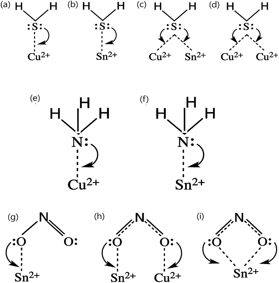 | ||
| Fig. 55 The electron transfer mechanism of (a–d) H2S, (e and f) NH3 and (g–i) NO2 molecules on the [001] surface of CTS. [Reprinted with copyright permission from ref. 106.] | ||
The low cost, simple device structure and efficient operation at room temperature makes CTS an ideal material for gas sensing applications. However, the gas sensing efficiency and dynamic response of CTS based gas sensors are still low as compared to those of available commercial gas sensors. Possible strategies such as using suitable sensitizing elements (Pt, Ag, Au and Pd) and novel ‘n-type’ layers must be explored. In addition, various factors (both physical and chemical factors of the sensing element) influencing the sensing performance and the underlying gas sensing mechanism must be studied to enhance the performance of CTS based gas sensors.
3.4 Energy storage
The rising global energy demand and the need for cleaner sources of energy have kick-started a revolution in the research area.250–252 Renewable sources of energy like solar, wind, tidal, etc. are being focused upon extensively to reduce or eliminate the dependence on the limited and polluting fossil fuels.253–256 However, whatever may be the energy source, storage is a vital area of interest in today's scenario. Portable devices, energy on-demand applications and the erratic nature of renewable energy sources make batteries and supercapacitors a suitable choice for energy storage.257–261Li-ions, as the name suggests, forms the heart of the battery.263 The basic working principle of the battery is dependent on the repeated back and forth movement of Li-ions between the cathode and anode.264 The anode is the negative electrode and releases Li ions during the discharging process to be absorbed by the cathode, which is the positive electrode. The ions are transported between the electrodes by the electrolyte. The major components of the battery are the (1) anode (2) cathode (3) separator and (4) electrolyte. Commercial batteries use graphite as an anode.264 The structure, surface area, ability to accommodate Li ions into its structure, cost and natural abundance make graphite as an ideal anode material. There are some other materials such as transition metal oxides (TMOs), which are suitable anode materials.265–268 To determine the performance of materials as an electrode material, parameters such as reversible/irreversible capacity, stability, coulombic efficiency and rate capacity are considered. Ideally, the reversibility of the electrode, i.e. charge insertion/de-insertion should be 100%, but that is not the case due to numerous losses.269–271 The major loss is due to the formation of a solid electrolyte interface (SEI) layer.272 This is a boon and bane because the layer formed on the surface of the electrode during the first cycle of the battery consumes Li-ions but protects the electrode from solvent damage. The stability of the electrode is an important factor. The electrochemical stability of the electrode is highly influenced by the chemical and physical stability of the material.273–276 The electrode is subjected to repeated charging and discharging cycles. The capacity of the electrode fades over time/cycles due to various factors such as structural degradation, incomplete insertion/de-insertion of Li ions and other losses.277,278 Coulombic efficiency refers to the discharge and charge capacity of the anode material. This also translates to the lithium removal to lithium insertion ratio. Thus, the porosity, surface area, and external factors affecting the mobility of the Li ions affect the coulombic efficiency. Rate capacity refers to the capacity retention of the material when subjected to charge–discharge cycles at different current densities. This ability of the material helps in achieving higher power density devices while maintaining higher energy density.
The anode plays a vital role in battery performance, and hence the properties of the anode material need to be considered during the fabrication of batteries. The morphology, size, shape, crystallinity, etc. of the material have a severe effect on the performance of the electrode. Currently, carbon, silicon, and TMOs are available as anode materials.279–286 Carbon-based anode materials are classified into two types: graphitic and non-graphitic carbon. Graphite is the most popularly used anode material.287 The theoretical capacity is 372 mA h g−1 which is lower than other types of anode materials.288 Metal sulfides are being investigated as an active material in Li-ion batteries due to their high energy density and natural abundance.289–291 Theoretical capacities of metal sulfides such as FeS2, MoS2, Bi2S3, etc. are much higher than those of currently used metal oxides and carbon electrodes.292–294 Tin based materials have been reported in the past due to their higher capacity.295,296 However, the major problem is the volume expansion and contraction during the lithiation and de-lithiation process, which significantly hampers the structural stability, and in turn the capacity.297 Volume expansion–contraction up to 400% has been observed, which contributes towards fast capacity fading and large initial capacity loss.298 To overcome this problem, many solutions have been proposed. Preparation of porous electrode materials, higher electronic conductivity, the inclusion of a matrix material (CNTs, RGO, graphene, etc.) and incorporation of metals such as copper to inherently modify the structure are some of the viable solutions.299–301 The basic idea of introducing Cu is to increase the crystal structure volume, which helps in the accommodation of Li ions without inducing a significant stress on the structure. Introduction of Cu also improves the electronic conductivity and interlayer spaces and the tunnels in CTS system which facilitates unhindered diffusion of Li ions.302
CTS belongs to the important category of I–V–VI ternary chalcogenide materials having applications in various fields. In this section, we discuss the energy storage application of CTS compounds. CTS can be employed as an anode material in Li-ion batteries. The schematic structure of the typical CTS based Li-ion battery is shown in Fig. 56(a). The CV scan of CTS suggests at least two electrochemical reactions taking place (Fig. 56(b)). For the first cathodic scan of the material, two peaks in the 0.6–0.8 V and 1.0–1.2 V regions correspond to lithiation and formation of Cu, Sn, and Li2S, respectively. Similarly, within the potential range of 0.5 V–0.0005 V there is alloying of Sn and Li. The corresponding dealloying peak is centered at 0.6 V in the anodic cycle. During the anodic cycle, the oxidation of Sn and Cu occurs at ∼1.9 V and 2.3 V.
 | ||
| Fig. 56 (a) The schematic structure of the typical CTS based Li-ion battery and (b) the cyclic voltammograms (CVs) of the CTS based Li-ion battery. [Reprinted with copyright permission from ref. 91.] | ||
The following electrochemical reactions help in understanding the underlying process during the charge and discharge cycle.
| Cu2SnS3 + 6Li+ + 6e− ↔ 2Cu + Sn + 3Li2S | (9) |
| Sn + xLi+ + xe− ↔ LixSni, (0 ≤ x ≤ 4.4) | (10) |
| 6C + xLi+ + xe− ↔ LixC6 | (11) |
Nie et al.86 reported successful synthesis of single crystal ternary thiostannate (H3O)2(enH2)Cu8Sn3S12 (CTS) by a surfactant thermal method and its application in Li batteries. The FESEM image of the synthesized single crystal ternary thiostannate is shown in Fig. 57(a). An icosahedral cluster (Cu8S12)16− structure of 3D anionic open frameworks consisting of disordered charge balanced species of H2en2+ and H3O+ were obtained (Fig. 57(b and c)). These disordered charge balanced species serve an important purpose of structural stability for larger electrochemical cycles. The structure of CTS plays an important role in the fast diffusion of Li+ ions. The icosahedral cluster forms the building block for 3D CTS with large interspaces and channels for efficient Li ion penetration. A first cycle discharge capacity of 1385 mA h g−1 was observed with a subsequent charge capacity of 870.3 mA h g−1 (Fig. 57(d)). The high value of capacity can be attributed to the overall electrolyte – active material contacts, short diffusion distance and large Li ion storage arising from the 3D nano-channels in the CTS structure. The electrode exhibited 563 mA h g−1 capacity at 100 mA g−1 current density and good cycling stability (7.2% loss from 5–100 cycles). The enhanced cycling performance could quite possibly be due to the 3D open structure, which allowed volume expansion during lithium insertion and prevented the structural collapse. Almost 100% coulombic efficiency (Fig. 57(e)) was obtained suggesting that the nano-channels and tunnels present within the structure allow unobstructed movement of Li ions.
 | ||
| Fig. 57 (a) The FESEM image of single crystal ternary thiostannate, (b and c) the icosahedral [Cu8S12]16− cluster and its connectivity with six Sn4+ ions with ball and stick mode and polyhedral mode, respectively, (d) the charge and discharge curves of CTS at a current density of 0.1 A g−1 and (e) the capacity as a function of cycle numbers at a current density of 0.1 A g−1. [Reprinted with copyright permission from ref. 86.] | ||
Qu et al.87,88 synthesized CTS mesoporous spheres Fig. 58(a) and 3D cabbage-like nanostructures Fig. 58(b)via a solvothermal method. The electrochemical performance confirms high initial charge–discharge capacities in both the cases with a slight increase in capacity for the cabbage-like nanostructure electrode.
 | ||
| Fig. 58 (a and b) The FESEM image of CTS mesoporous spheres and 3D cabbage-like nanostructures, respectively, and (c and d) the charge–discharge curves of CTS mesoporous spheres and 3D cabbage-like nanostructures at a current density of 100 mA g−1, respectively. [Reprinted with copyright permission from ref. 87 and 88.] | ||
Mesoporous CTS exhibits a first discharge capacity of 913 mA h g−1 and a subsequent charge capacity of 891 mA h g−1Fig. 58(c). Due to the porous nature of the CTS electrode and the spherical shape, the initial capacity is high, but eventually, the capacity fades to 411 mA h g−1 after 50 cycles. The absence of a rigid nanostructure and probable coalescence of CTS particles during cycling may have resulted in the capacity loss. A cabbage-like nanostructure is formed of several nanosheets bunched together. The center portion is denser than the edge portion. The 2D nanosheets oriented in different directions provide larger surface area. This results in an efficient electrolyte contact. The initial lithiation capacity was 1021 mA h g−1, and de-lithiation capacity was 842 mA h g−1Fig. 58(d). However, there was a significant increase in the cycling performance. The cabbage-like nanostructure electrode has a significantly higher capacity retention of 621 mA h g−1 after 50 cycles. The distance between the nanosheets is significant enough to negate the coalescence effect that may have occurred in the mesoporous spheres. This helps to maintain the structural integrity of the material and cycling stability. Additionally, the cabbage-like nanostructure electrode exhibited a higher surface area (22.4 m2 g−1) and pore size (13.8 nm) than the mesoporous sphere electrode (19.9 m2 g−1 and 10 nm) which accounted for higher Li+ ion interaction and accommodation. Thus, the electrochemical performance is influenced by the electrode microstructure. The above results indicate that CTS has improved performance and stability compared to the parent tin sulfide electrode. Various strategies have been adopted to enhance the performance of the electrode.299–301 One of the strategies, such as fabrication of composite electrodes, i.e. the combination of an active electrode with RGO, graphene and other carbon materials, has been found to improve the performance and can be suitably applied for CTS electrodes.
Tao et al.,89 with the facile hydrothermal synthesis of CTS and a CTS/RGO composite, have demonstrated that stability can be improved from 20% for CTS to 80% for the RGO/CTS composite after 100 cycles. The initial lithiation and de-lithiation charge capacities were 1066 mA h g−1 and 621 mA h g−1 for CTS (Fig. 59(a)), while for RGO/CTS they were 1200 mA h g−1 and 704 mA h g−1 (Fig. 59(b)), respectively. The capacity fades to 124 mA h g−1 after 100 cycles for CTS and 561 mA h g−1 for RGO/CTS. Higher cycling capacity retention results from inclusion of a robust composite structure and the synergistic effect of CTS and RGO. The addition of RGO does not only increase the conductivity of the composite as a whole but also improves electronic interconnectivity between CTS nanoparticles which is evident from the EIS data as shown in Fig. 59(c). Additionally, as seen from the FESEM images, the synthesized CTS nanoparticles are aggregated, Fig. 59(d), while CTS/RGO composite exhibits homogeneous nanoparticle distribution without any particle aggregation (Fig. 59(e)) resulting in maximum exposure of surface area for an enhanced electrochemical activity.
 | ||
| Fig. 59 (a and b) The charge–discharge curves of CTS and the CTS/RGO composite at a current density of 100 mA g−1, respectively, (c) the Nyquist plots of CTS and the CTS/RGO composite after 3 cycles and (d and e) the FESEM images of CTS and the CTS/RGO composite. [Reprinted with copyright permission from ref. 89.] | ||
Zhang et al.90 attempted a hydrothermal synthesis of CTS hollow microspheres with Na2EDTA as a chelating agent. Na2EDTA was used to steadily release Cu and Sn ions in the system to react with S and simultaneously act as a template to form hollow microspheres. During the first discharge cycle, the electrode exhibits a capacity of 1316 mA h g−1 and 455.2 mA h g−1 in the next charging cycle (Fig. 60(a)). The loss in capacity is credited to the formation of an insulating Li2S layer on the surface of the material. The spherically shaped particles are also more susceptible to coalescence, and that is exhibited in the cycling capacity of 190 mA h g−1 after 50 cycles (Fig. 60(b)). The drastic loss in capacity was mitigated in their next attempt wherein they combined RGO with CTS to provide structural stability and enhancement in electronic property.91 The CTS hollow microspheres were anchored to RGO sheets forming a composite electrode. The initial lithiation and delithiation capacities increased to 1514 mA h g−1 and 1077 mA h g−1, respectively, (Fig. 60(c)). Addition of RGO also boosted the rate capacity performance. Even at 1000 mA g−1 current density, the charge capacity is 228 mA h g−1, about 50% of the value at 200 mA g−1 (Fig. 60(d)).
 | ||
| Fig. 60 (a and b) The charge–discharge curves and cyclic behaviour of the CTS electrode at a current density of 100 mA g−1, respectively, and (c and d) the cyclic behaviour (at a current density of 100 mA g−1) and the rate capability (at different current densities) of CTS and the CTS/RGO electrode, respectively. [Reprinted with copyright permission from ref. 90 and 91.] | ||
Incorporation of RGO has such a profound effect on the performance of the CTS composite electrode that it is only logical that other combinations need to be tried out. Graphene has better electrochemical performance than RGO.303 Fu et al.92 encapsulated CTS nanoparticles in graphene sheets and tested it as an anode electrode. The rate capability of the electrode was exceptionally high, and even at 1000 mA g−1 current density, it delivered 805 mA h g−1 (approximately 1000 mA h g−1 at 100 mA g−1). The electrode could retain 69% of its initial capacity at 1000 mA h g−1 after 100 cycles and 89% at 500 mA g−1 after 300 cycles. As is well documented, graphene has high electronic conductivity and surface area, which contribute immensely towards the high capacity and rate capability of the electrode.304 Graphene sheets provide structural strength to counter the degradation due to volume expansion and contraction during the charge–discharge cycle.305 The electrolyte ion size and the electrode interlayer distance and tunnel size are the decisive factors that regulate the electrochemical performance. In particular, the interlayer distance of Cu2SnS3 (CTS) is 2.280 Å,93 which is quite higher than the radius of Li-ions and thus can accommodate more Li-ions reflecting itself as an ideal material for Li-ion battery applications. However, the higher cost of Li is a limiting factor for mass scale production.306
As an effective substitute, Na ion batteries have gained significant interest because of their low cost and similarities to Li-ion batteries.307 Additionally, the radius of Na ions is quite low (1.12 Å) which promotes easy diffusion through the CTS crystal structure.308 Very few reports93,94 are available on CTS based Na ion batteries as the research based on it is in the primitive stage. Solvothermally synthesized CTS nanosheets93 exhibited an initial discharge (586 mA h g−1) and charge capacity (351 mA h g−1) at a current density of 30 mA g−1 while an improved initial discharge (696.8 mA h g−1) and charge capacities (477.7 mA h g−1) at a current density of 100 mA g−1 were obtained for the post-annealed (500 °C–4 h in an argon atmosphere) flower-like CTS nanostructures obtained using a solvothermal technique.94 The enhanced performance was attributed to the post-annealing treatment which improved the nanostructure crystallinity and thus the electrical conductivity. As the obtained CTS results are close to its theoretical specific capacity (763.8 mA h g−1), a scope for development still exists. The reported results of CTS based Li and Na ion batteries are summarized in Table 7.
| Material | Method | Morphology | Study content | Results | Ref. | |||
|---|---|---|---|---|---|---|---|---|
| Current density mA g−1 | DC mA h g−1 | CC mA h g−1 | CR mA h g−1 | |||||
| (H3O)2(enH2) Cu8Sn3S12 | Surfactant method strategy | Porous structure with 3D open frameworks | Investigation of ternary thiostannate for Li ion batteries | 100 | 1385 | 870 | 563–100 cycles | 86 |
| Cu2SnS3 | Solvothermal (180°C–20 h) | Mesospheres (200 nm), surface area: 19.9 m2 g−1 pore size: 10 nm | Electrode synthesis and its performance evaluation in Li ion batteries | 100 | 913 | 891 | 411–50 cycles | 87 |
| Cu2SnS3 | Solvothermal (180 °C–15 h) | A 3D cabbage-like porous network, surface area: 22.4 m2 g−1 pore size: 13.8 nm | Electrode synthesis and its performance evaluation in Li ion batteries | 100 | 1021 | 842 | 621–50 cycles | 88 |
| Cu2SnS3/RGO | Hydrothermal (180 °C–24 h) | CTS: aggerated nanoparticles (100 nm) CTS/RGO: homogeneous nanoparticles without aggregation (5–10 nm) | Electrode synthesis and its performance evaluation in Li ion batteries | 100 (CTS) | 1066 | 621 | 124–100 cycles | 89 |
| 100 (CTS/RGO) | 1200 | 704 | 561–100 cycles | |||||
| Cu2SnS3 | Hydrothermal (180 °C–24 h) using Na2EDTA as a complexing agent | Hollow microspheres (1–1.2 μm) | Electrode synthesis and its performance evaluation in Li ion batteries | 100 | 1316 | 455.2 | 190–50 cycles | 90 |
| Cu2SnS3/RGO | Hydrothermal (180 °C–24 h) using Na2EDTA as a complexing agent | CTS micropheres (450 nm) anchored on RGO | Electrode synthesis and its performance evaluation in Li ion batteries | 100 (CTS) | 1066 | 621 | 124–100 cycles | 91 |
| 100 (CTS/RGO) | 1200 | 704 | 561–100 cycles | |||||
| Cu2SnS3/RGO | Liquid phase method | Spheres | Electrode synthesis and its performance evaluation in Li ion batteries | 500 | 1043.1 | 692 | 178–50 cycles | 92 |
| Cu2SnS3 | Solvothermal (220 °C–24 h) | Nanosheets (1–2 μm) | Electrode synthesis and its performance evaluation in Li ion batteries | 30 | 586 | 351 | 178–50 cycles | 93 |
| Cu2SnS3 | Solvothermal (180°C–16 h) then annealed 500 °C–4 h in an argon atmosphere | Flower-like spheres (1 μm), highly crystalline spheres, are obtained | Electrode synthesis and study of the effect of crystallinity on the performance of Na ion batteries | 100 | 696.8 | 477.7 | 200–50 cycles | 94 |
Thus, the initial reports show that CTS is a suitable anode material for Li batteries. The morphology, 3D nanostructures, etc. affect the capacity of the CTS electrode. Different nanostructures, which promote shorter ion diffusion lengths and interconnectivity, need to be investigated. Recent investigation309 reveals that a small particle size and small grain size have a significant effect on the performance of the electrode. As the size shrinks, small size effect comes into play, which improves the electrical conductivity as well as certain physical characteristics. It is no secret that nano-sized particles also increase the surface area as well. The electrolyte and nano-sized particle interface have, therefore, stronger Li-ion adsorption on the surface. The small particle size also shortens the ion diffusion distance. The porosity and surface area of the anode electrode are also critical parameters, which influences the capacity. Porous materials expose a large surface area of the material to the electrolyte thus maximizing the electrochemically active sites. However, making a material highly porous may have an adverse effect on the volumetric capacity of the material. The CTS charge storage mechanism shows that the process involves the formation of a Li–Sn alloy. The main problems involved are poor electronic conductivity and dramatic volume change during lithium intercalation and de-intercalation. Composite electrodes have a robust structure, and careful combinations can improve the performance of the electrode due to the synergistic effect of materials. The matrix material can be used to contain CTS and support it. The irreversible capacity loss is usually attributed to the formation of an insulating Li2S layer, and hence studies focusing on overcoming this problem should be conducted.310 None of the reports have focused on this issue. However, this can be one of the leading causes of the irreversible capacity loss. Similarly, particle aggregation should be focused upon during cycling studies. The matrix material may shield the electrode from this problem, but not much evidence has been provided in the reports to refute the contribution of this loss.
Various electrode properties such as electronic conductivity, surface area, and porous structure form the backbone of supercapacitors.315 The higher electrical conductivity provides faster charge transport for efficient redox reactions while the high surface area porous structure decides the amount of charge stored and propagated through the electrode. Various materials such as conducting polymers,316,317 metal oxides318,319 and carbon-based compounds320,321 have been extensively researched for supercapacitor applications. Recently, transition metal sulfides have been studied and applied in supercapacitor applications.322–324 Metal sulfides exhibit lower electronegativity which is highly suitable for electrochemical applications. Additionally, compared to single metal sulfides, ternary metal sulfides exhibit multiple oxidations states which could contribute an active redox activity.325 Considering the viability of metal sulfides for supercapacitor applications, Wang et al.95 first studied the electrochemical behavior of the Cu2SnS3 (CTS) electrode for supercapacitor applications. The effect of different CTS microstructures on the supercapacitive performance was evaluated. CTS nanoparticles and microspheres were synthesized using a solvothermal technique and mixed with acetylene black and polyvinylidene fluoride (PVDF) in 1-methyl-2-pyrrolidinone to form a slurry paste. The slurry paste was then coated on a nickel foam (NF) substrate and dried at 60 °C for 12 h to form an active electrode. Fig. 61(a and b) show the FESEM images of CTS nanoparticles (N-CTS) and microspheres (M-CTS). As seen, the agglomerated nanoparticles with the size of 30 nm and the microspheres composed of overlapping nanosheets in the size range of 600–650 nm are formed in N-CTS and M-CTS, respectively.
 | ||
| Fig. 61 The FE-SEM image of (a) N-CTS nanoparticles and (b) M-CTS microspheres. [Reprinted with copyright permission from ref. 95.] | ||
The cyclic voltammetry (CV) studies conducted in 3 M KOH solution in the potential range of 0.15–0.65 V are depicted in Fig. 62(a and b) and reveal the pseudocapacitive nature of the synthesized CTS electrodes due to the presence of prominent redox peaks.
 | ||
| Fig. 62 (a) CV curves of the N-CTS; (b) CV curves of the M-CTS; (c) GCD curves of the N-CTS at different current densities; (d) GCD curves of the M-CTS at different current densities. [Reprinted with copyright permission from ref. 95.] | ||
For the N-CTS electrode, the CV curves at/above 40 mV scan rate became less obvious (the corresponding area under the curves reduced) due to the sluggish kinetics of the electrode at higher scan rates. As for the M-CTS electrode, the CV curves increased proportionally (higher attainable current densities) with the increased scan rate indicating efficient reversibility for the rapid redox reactions. As the capacitance is directly proportional to the area under the CV curve, the M-CTS electrode exhibited a higher capacitance than the N-CTS electrode. Also, the switching to cathodic and anodic currents and vice versa is rapid indicating no development of the concentration gradient within the solid electrode structure. The corresponding galvanostatic charge–discharge (GCD) study also reflected a similar result. As seen from the corresponding GCD curves in Fig. 62(c and d), the M-CTS exhibits a higher discharge time than the N-CTS electrode indicating its higher specific capacitance. The specific capacitance of the N-CTS electrode at GCD densities of 1, 2, 4, 8, 10, 15 and 20 A g−1 are 313, 288, 255, 218, 201, 157, and 126 C g−1, respectively, while an enhanced specific capacitances of 406, 349, 330, 276, 253, 115, and 101 C g−1 are obtained for the M-CTS electrode. Compared to the N-CTS electrode, the M-CTS electrode exhibited an enhanced performance and was attributed to its obtained morphology. The M-CTS electrode had a nanosheet-assembled microsphere-like morphology with large surface area (44.9 m2 g−1) than the N-CTS electrode nanoparticle-like morphology (28.2 m2 g−1). The high surface area morphology, as mentioned before, provides stupendous electroactive sites for rapid redox reactions and thus contributes to an improved capacitive performance.
Thus, the morphology regulated CTS electrode exhibited a maximum specific capacitance of 406 F g−1 with an energy density of 85.6 W h kg−1 and a power density of 720 W kg−1 in 1 M KOH electrolyte. Additionally, the electrode cycling stability is also an essential parameter for the practical application of the supercapacitor. The CTS electrode exhibited 60% stability retention for 2000 cycles which could be considered low as compared to those of other reported materials.315 The mediocre performance of the CTS electrode regarding its lower capacitance and lower cycling stability could be attributed to the use of a binder which may introduce electrical resistance in the ionic transport system of the electrode. Binders are well known for hampering the electrochemical performance of the electrodes.192 Hence, a strategy for obtaining binder-free electrode materials can help in improving the supercapacitive performance of the electrode. Additionally, the electrical properties of the electrode material are also important. Thus, binder-free electrodes combined with high surface area morphology and high electrical conductivity will surely help in achieving a high supercapacitive performance.
Considering this approach, Lokhande et al.96 obtained the direct deposition of Cu rich Cu4SnS4 (CTS) thin film electrode by the SILAR technique on nickel foam (NF) and successfully achieved an enhanced supercapacitive performance. The synthesized Cu rich CTS electrode exhibited an orthorhombic crystal structure with a hydrophilic surface and a porous morphology (Fig. 63(a)). The hydrophilic surface coupled with porous morphology promoted an effective electrode–electrolyte interaction and utilization of the electroactive sites while the orthorhombic crystal structure provided a larger unit cell volume (669.94 Å3) favorable for larger ionic migration. Additionally, the random distribution of atoms and inconsistent bonding between Sn–S in the crystal structure promoted an easy charge transfer and redox mechanism. Thus, the synergistic effect of efficient charge transfer, binder-free compounds with a hydrophilic surface and higher electrical conductivity with larger cell volume resulted in a higher capacitance of 704 F g−1 with an energy density of 27.77 W h kg−1 and a power density of 7.14 kW kg−1 in 1 M NaOH electrolyte (Fig. 63(b and c)). In work, 1 M NaOH electrolyte was used while in a previous study,95 1 M KOH electrolyte was used. The lower ionic radius of Na+ ions (0.102 nm) than K+ ions (0.138 nm) promoted higher electrolyte–electrode interaction resulting in superior capacitance. Thus, appropriate electrolyte selection is vital for achieving higher capacitance. Furthermore, the authors extended the work by fabricating a solid state symmetric device using CTS electrodes and polymer gel electrolyte (PVA/NaOH). The device exhibited a specific capacitance of 34.9 F g−1 with an energy density of 2.4 W h kg−1 and a power density of 0.291 kW kg−1 with nearly 90% capacity retention for 1000 cycles (Fig. 63(d and e)). The actual device demonstration was accomplished by charging the device using a constant power source and discharging using a light emitting diode (LED) (Fig. 63(f)). However, the fabricated device exhibited an average performance as compared to the other well-established electrode materials. Additionally, if the CTS electrodes are integrated with carbon-based composites (carbon nanotubes, graphene, and reduced graphene oxide), further improvement in supercapacitive performance due to their higher electrical conductivity and larger surface area can be expected. As the literature based on the supercapacitive study of the CTS electrode is very limited, additional studies focusing on influential factors that affect the electrochemical performance are desired.
 | ||
| Fig. 63 (a) The FESEM image of the CTS nanoparticle thin film on the NF substrate, (b and c) the CV and the corresponding GCD curves of the CTS electrode in 1 M NaOH electrolyte at varied scan rates and current densities, respectively, (d and e) the CV curves of the fabricated device at varied scan rates in a fixed potential window (1.2 V/SCE) and the corresponding stability plot for 1000 CV cycles (the inset shows the CV curves), respectively, and (f) the actual photograph of the symmetric device demonstration. [Reprinted with copyright permission from ref. 96.] | ||
Thus, CTS has demonstrated its successful application as an electrode material in supercapacitor applications. The fabricated device exhibited an average performance as compared to other well-established electrode materials. The lower device capacitance and mediocre cycling stability are the major performance limiting factors. As a possible solution, the CTS electrode can be integrated with carbon-based composites (CNTs, GO, and RGO) for performance improvement due to their high electrical conductivity, large surface area and stable structure. In addition, various influential factors such as the electrode structure, microstructure, conductivity and electrolyte (type and concentration) should be studied.
3.5 Other applications
Apart from the above discussed applications, CTS has been applied in various other applications which are discussed below.Motivated by this, Lokhande et al.108 successfully demonstrated the antibacterial activity of CTS nanoparticles against Gram-positive (S. aureus) and Gram-negative (E. coli) bacterial strains. The CTS nanoparticles (10–12 nm) were synthesized using a cost-effective hot injection technique and tested for antibacterial activity against pathogenic stains by determining the zone of inhibition (ZOI). The antibacterial activity was tested by the agar-well diffusion method. Fig. 64(a and b) show the ZOI of CTS nanoparticles for E. coli and S. aureus after 24 h incubation. As seen, a clear ZOI is observed for E. coli (22 mm) and S. aureus (15 mm) strains. The difference in the ZOI is attributed to the different cell membrane structures and cell wall thicknesses of the bacteria. The cell wall thickness of E. coli is approximately 10 nm, and S. aureus is 80 nm.332 The thicker cell wall resists the nanoparticle diffusion and its related attack on the cell membrane thereby protecting the cytoplasmic fluid and the bacteria. Hence, the obtained ZOI for S. aureus was smaller than that for E. coli.
 | ||
| Fig. 64 The photographs of the zone of inhibition (ZOI) of CTS nanoparticles for (a) Gram-negative (E. coli) and (b) Gram-positive (S. aureus) bacteria. [Reprinted with copyright permission from ref. 108.] | ||
To get a clear view of the antibacterial activity, the FESEM images of the reference and CTS nanoparticle treated bacteria are shown in Fig. 65(a–l). As seen, the reference (untreated) E. coli bacteria exhibited a smooth and uniform cell texture with an average cell length and a cell width of 3.2 μm and 1.24 μm, respectively. As for CTS nanoparticle treated bacteria, a significant disruption in the cell dimensions are observed. The cell texture was non-uniform and rough, and the average width is reduced to 0.9 μm while the cell length was increased to 6 μm. Additionally, as seen from the images, bacterial death is associated with extrusion of intracellular fluids thereby rendering the cell membrane structure with intricate shapes (shriveled and deflated structures). Likewise, a similar effect of varied cell dimensions and structures is observed for S. aureus bacteria. The reference bacteria exhibit a smooth and uniform spherical texture with an average cell diameter of 0.7 μm while the CTS nanoparticle treated bacteria exhibits an enlarged cell diameter (1.2 μm) due to the restricted cell division mechanism. Moreover, the CTS nanoparticle treated bacteria exhibited ruptured cell membrane structures due to the extruded cytoplasmic fluids. Thus, as seen from the results, the bacterial cell death is associated with the direct damage to the cellular membrane induced through the cytoplasmic fluid extrusion by CTS nanoparticles.
 | ||
| Fig. 65 The FE-SEM images of E. coli bacteria (a and b) without CTS nanoparticle treatment and (c–f) with CTS nanoparticle treatment and the FESEM images of S. aureus bacteria (g and h) without CTS nanoparticle treatment and (i–l) with CTS nanoparticle treatment. [Reprinted with copyright permission from ref. 108.] | ||
Several mechanisms for the antibacterial activity of the nanoparticles such as the formation of reactive oxygen species (ROS) that impose oxidative stress on the cellular structure, release of metal ions leading to complex formation with the phosphate/thiol groups in the nucleic acid and direct nanoparticle-cell membrane interaction have been proposed.329,333,334 Based on the obtained results, the authors concluded a plausible mechanism of electrostatic interaction between CTS nanoparticles and the bacteria. It is well known that the bacterial cell wall has a net negative charge while the synthesized CTS nanoparticles in the study has a net positive charge as evaluated for the isoelectric point zeta potential study. Thus, the electrostatic attraction between the opposite charges resulted in a nanoparticle-bacterial cell membrane interaction. The CTS nanoparticles form strong bonds with carboxyl, amino and thiol groups of the bacterial membrane and impart damage leading to the extrusion of cytoplasmic fluids, DNA and other genetic compounds resulting in restricted cell replication and death. Additionally, the smaller size of CTS nanoparticles (10–12 nm) promoted larger surface area interaction with the bacterial membrane for efficient antibacterial activity. Thus, the direct interaction between CTS nanoparticles and bacterial cell membrane is the driving mechanism of the antibacterial activity (Fig. 66). Furthermore, of note, Cu is a well-known antibacterial agent, and the release of Cu ions from CTS nanoparticles could also be a possible reason for the antibacterial activity.335 However, the actual antibacterial mechanism is still unclear and hence extensive studies for detailed understanding of the interaction between CTS particles and bacteria are needed to realize its future role as a biocidal agent.
 | ||
| Fig. 66 The schematic representation of the mechanism of the antibacterial activity of CTS nanoparticles. | ||
Thus, it can be concluded that CTS exhibits strong antibacterial activity against both Gram positive and negative bacteria. The non-toxic nature, low cost and easy processability makes CTS nanoparticles an ideal candidate material for biocidal applications. However, the exact mechanism of the antibacterial activity of CTS nanoparticles is still unclear. Also, the actual use of CTS nanoparticles in the human biosystem is unknown as cytotoxicity studies of CTS nanoparticles are not conducted to verify its compatibility with the human biosystem. Hence, further detailed studies are required to understand the exact role and nature of CTS nanoparticles for antibacterial activities.
The electrochemical water-splitting processes namely the HER and OER must be carefully understood. Compared to the OER, the HER is a rapid process as it involves only two electron transfer reactions, while the OER process is associated with four electron–proton reactions and thus it is referred to as a ‘kinetically sluggish’ process.338 To accelerate the reaction process, a higher overpotential (higher energy) is needed to overcome the kinetic barrier for activating the electrocatalyst. However, employing higher overpotential results in reduced overall electrocatalyst efficiency. Thus, an efficient electrocatalyst is needed that will lower the overpotential and achieve the desired catalytic activity. Usually, the performance of an electrocatalyst is measured in terms of the amount of gas liberated or the overpotential achieved for the catalytic activity. The aspect of measuring the gas liberated is complex and costly as it requires sophisticated instruments and techniques (gas chromatography). On the other hand, the following aspect of calculating the overpotential is simple and easy. Generally, the electrocatalytic efficiency is measured as the overpotential required to attain a current density of 10 mA cm−2, which is equivalent to 10% solar to hydrogen conversion efficiency for water-splitting.339 The ideal voltage of water splitting is 1.23 V. Any voltage exceeding this value is termed ‘overpotential’. Hence, the overpotential value should be as low as possible for an efficient electrocatalyst. Additionally, the Tafel slope, which determines the reaction kinetics of the catalyst, should be low. The Tafel slope reflects the inherent properties of the catalyst.101,102 A Tafel slope value close to 40 mV dec−1 indicates that a two-electron transfer is the rate determining step. A value close to 60 mV dec−1 corroborates a rate-limiting step that follows the first electron transfer while a value close to 120 mV dec−1 suggests a single-electron transfer step without a pre-equilibrium step.102 As the electrocatalysis process is based on the applied bias induced water-splitting, the electrical resistance of the active electrode (charge transfer resistance) should also be as low as possible. The schematics of electrochemical water-splitting setup are shown in Fig. 67.
 | ||
| Fig. 67 The schematics of the electrochemical water-splitting setup. | ||
Various precious materials such as Pt, RuO2, and IrO2 have been employed as an electrocatalyst due to their superior performance regarding lower overpotential and faster reaction kinetics.339 However, the higher cost and scarcity of the employed elements restrict their commercial applications. Hence, research in pursuit of non-precious, earth-abundant, low-cost and efficient electrocatalysts is important. Various materials such as metals,340,341 nitrides,342,343 oxides,344,345 oxyhydroxides,346,347 phosphides348,349 and carbides350,351 have been studied due to their electrocatalytic activities. Recently a new class of materials namely transition metal chalcogenides (MoS2, CoS2, CoSe2, FeS2, and WS2) have been developed for HER electrocatalytic activity.352–361 The outcome of the reports concluded that HER activity could be improved by (1) synthesizing layered metal chalcogenides which provided enhanced active edges and surface area, (2) employing carbon-based materials like carbon nanotubes (CNTs) and graphene for improving the electrical conductivity and (3) increasing sulfur atom density on the metal chalcogenide surface. The increased sulfur atoms on the metal chalcogenide surface are unsaturated, and thus they act as an effective center for –OH and H2O ligands for efficient water-splitting.
Thus, inspired by this, Maheskumar et al.103 studied the electrocatalytic HER activity of the CTS electrode. In the study, a comparison between the HER activity of sulfur-rich Cu2SnS3 (CTS-A) and sulfur poor Cu4SnS4 (CTS-B) particles synthesized by a solvothermal technique was conducted. The synthesized CTS catalyst powder was finely crushed and mixed with a solution of 5 wt% Nafion in ethanol solvent (Nafion/ethanol: 1:10) for 30 min to form a homogeneous suppression. The formed suppression was then drop-cast on a glassy carbon (GC) electrode followed by room temperature overnight drying. The dried CTS coated GC was used as the working electrode, Pt as the counter electrode and a Ag/AgCl electrode as the reference electrode and the electrochemical study was conducted in 0.5 M H2SO4 solution. Fig. 68(a and b) show the FESEM images of the synthesized CTS-A and CTS-B particles, respectively. As seen, the presence of a layered structure with particle aggregation is visible for CTS-A while irregular particles with a wider size range are observed for CTS-B. The elemental atomic composition (at%) was found to be a sulfur-rich composition (Cu:Sn:S – 31:18:51) for CTS-A and sulfur poor composition (Cu:Sn:S – 46:9:45) for the CTS-B electrode. The estimated bandgap values of 1.55 and 1.20 eV are obtained for CTS-A and CTS-B electrodes, respectively. The increased bandgap of the CTS-A electrode was due to the presence of higher sulfur content which effectively raises the conduction band from the Fermi level. Based on the bandgap values and the conduction band potentials, the band diagram is obtained (Fig. 68(c)).
 | ||
| Fig. 68 (a and b) The FESEM image of CTS (A) and CTS (B), respectively, (c) the schematic diagram of band structures of CTS (A) and CTS (B) and (d) the comparative PL spectra of CTS (A) and CTS (B). [Reprinted with copyright permission from ref. 103.] | ||
As seen from the band diagram, the conduction band of the CTS-A electrode is above the conduction band of the CTS-B electrode due to the higher bandgap originating from higher sulfur content. Similar results of increased bandgap due to higher sulfur content have been reported in several studies based on CTS TFSCs.32,42 The existence of the CTS-B electrode conduction band in the higher positive potential in the RHE reflects its lower HER activity compared to the CTS-A electrode. Additionally, the PL spectra (Fig. 68(d)) also clearly indicated the higher charge recombination (higher structural defects) in the CTS-B electrode (higher peak intensity centered at 380 nm) as compared to the CTS-A electrode suggesting its reduced catalytic performance. The HER activity was evaluated from the polarization curve in the potential range of 0 to −1.25 V vs. RHE at 5 mV s−1 scan rate. As seen from the polarization curve (Fig. 69(a)), the CTS-A electrode exhibits a lower overpotential of 330 mV than the CTS-B electrode (358 mV) to achieve a current density of −10 mA cm−2. The Tafel plots (Fig. 69(b)) and EIS Nyquist plots (Fig. 69(c)) also signified the enhanced reaction kinetics and lower charge transfer resistance (Rct) of the CTS-A electrode (98 mV dec−1 and Rct: 25 ohm) than the CTS-B electrode (110 mV dec−1 and Rct: >100 ohm). The lower Tafel slope accompanied by lower charge resistance is a clear indication of an efficient electrocatalytic activity. The stability plot (Fig. 69(d)) also indicates a minor decrement in the catalytic performance after 500 cycles indicating the robust and durable nature of the electrodes. Thus, the CTS-A electrode, due to its higher sulfur concentration, resulted in favorable band alignment, reduced charge recombination (lower structural defects), reduced charge transport resistance and improved reaction kinetics resulting in an improved HER catalytic activity. Hence, it is clear that the sulfur concentration in the CTS compound plays a crucial role in influencing the electrocatalytic activity.
 | ||
| Fig. 69 (a) Polarization curves obtained for the GCE, CTS (A) and CTS (B); (b) the corresponding Tafel plots for CTS (A) and CTS (B), (c) the electrochemical impedance spectra of CTS (A) and CTS (B), (d) the polarization curve before and after 500 cycles stability tests of CTS (A) and CTS (B), at a scan rate of 100 mV s−1. [Reprinted with copyright permission from ref. 103.] | ||
The obtained overpotential of 330 mV for HER activity is very high and can be considered inefficient. However, in the following study, the same authors104 improved the performance by synthesizing Cu3SnS4 (CTS) with a uniform flowerlike microsphere morphology (Fig. 70(a)). The CTS electrode exhibits an efficient electrocatalytic performance with an overpotential of 230 mV, a Tafel slope of 76 mV dec−1 and superior stability for 2000 cycles (Fig. 70(b–d)). The enhanced catalytic performance is attributed to the morphology, which consisted of many intercrossed nanosheets. Thus, it is clear that the morphology also plays an important role in electrocatalytic activity.
 | ||
| Fig. 70 (a) The FESEM image of the solvothermally synthesized CTS electrode (CTS (S)), (b) the HER polarization curves for ball milled CTS electrode (CTS (B)) and solvothermally synthesized CTS electrode (CTS (S)) in comparison with bare GC and Pt/C electrodes, (c) the Tafel plots for CTS (B) and CTS (S) and (d) the polarization curves recorded initially and after 2000 cycles, at a scan rate of 100 mV s−1. [Reprinted with copyright permission from ref. 104.] | ||
Various other factors such as electrode electrical conductivity and structural configuration, which have been reported to influence the electrocatalytic performance of other electrode materials should also be considered in the case of the CTS electrocatalyst.354–359 The obtained overpotential value of the CTS electrode (220 mV) is still significantly higher than the well-established results of other electrocatalyst materials and can be considered ineffective.358,359 As very scanty data are available on the electrocatalytic study of the CTS electrode, further studies can shed more light on enhancing the performance of the electrocatalyst. Likewise, similar to the previously discussed photocatalytic performance of the CTS compound, the electrocatalytic performance is also influenced by the morphological and electrical properties of the electrode. A high surface area microstructure with higher electrical conductivity is desired for efficient performance. The electrode crystallinity should also be considered equally. Several literature reports have indicated that an amorphous electrode structure exhibits an efficient electrocatalytic activity than its crystalline counterparts due to the high density of coordinated unsaturated sites originating from the randomly oriented bonds.102,362 These unsaturated sites provide maximum interaction with the reactants and thus contribute for improved performance. Additionally, the surface wettability properties of the active electrode are important. The electrode should have a hydrophilic surface (contact angle < 90°) for maximum interfacial contact between the electrode surface and electrolyte. Hence, additional detailed studies are needed to examine and validate the impact of electrode properties on its electrocatalytic performance. The OER activity of the CTS electrocatalyst is still unexplored. If CTS electrocatalysts are well designed for efficient OER and HER catalytic activities, the bifunctional activity (overall water-splitting) of the CTS electrocatalyst could be effectively realized.
The surface wettability properties of (CTS) material were studied by Chang et al.107 In the study, a CTS thin film was deposited on a glass substrate by spin coating, and its wettability properties were studied and modified. The spin-coated CTS film on the glass substrate was annealed in an inert N2 atmosphere at various temperatures of 200, 300, 400 and 500 °C for 2 h. The scanning probe microscopy (SPM) images of the annealed CTS films are shown in Fig. 71(a–d) As seen from the images, the morphology and root mean square (RMS) roughness depend on the annealing temperature. The morphology transformed from a spiral-shaped embossment-like structure at 200 °C to a smooth and compact structure at 500 °C. Likewise, the RMS value is reduced from 8.440 nm at 200 °C to 0.432 nm at 500 °C confirming the formation of a smoother surface.
 | ||
| Fig. 71 SPM images of CTS films on glass substrates fabricated by spin-coating of CTS precursor solution: (a–d) annealed at 200, 300, 400, and 500 °C, respectively. [Reprinted with copyright permission from ref. 107.] | ||
The corresponding water contact angle values were found to be reduced with the increased annealing temperature (Fig. 72(a)).
 | ||
| Fig. 72 (a) The plot of the water contact angle vs. annealing temperature for the as-prepared CTS films. (b) Convertible switched surface wettability between amphiphilic and hydrophobic–lipophilic for the CTS film fabricated at 500 °C by modification with stearic acid and annealing at 300 °C. Cycle interval: 7 d. Inset: water and oil contact angle images. (c and d) Digital images for the antifogging properties of glass and CTS film coated glass samples (25 °C, 90% RH, air). The colorless transparent characteristic is because the film is ultra-thin. [Reprinted with copyright permission from ref. 107.] | ||
At 200 °C, the contact angle was greater than 45° which decreased to less than 1° at 500 °C. The higher contact angle value (>45°) at 200 °C was attributed to its spiral-shaped embossment-like structure morphology which acted as air pockets at the valleys, preventing it from complete wetting. At 500 °C, the contact angle was significantly reduced (<1°) due to the formation of a smooth surface with comparatively higher surface energy. Thus, a superhydrophilic CTS film was obtained at 500 °C which can be applied for the self-cleaning application. The surface of the CTS film annealed at 500 °C was modified by immersing it in stearic acid/ethanol (5 mM) solution for 12 h at room temperature followed by air drying at 50 °C for 10 min. The surface changed to a superhydrophobic (water contact angle: 109°) and superlipophilic (oil contact angle > 1°) surface due to reduced surface energy. Again, as the same film was annealed at 300 °C–2 h to remove the stearic acid, the film retained its superhydrophilic and superamphiphilic surface with a contact angle of <1°. Likewise, such a reversible wettability test was performed for 7 cycles until the developed internal defects became prominent in the film (Fig. 72(b)). Thus, the surface wettability of CTS films was varied and reproduced by modifying their microstructure/surface energy through annealing and stearic acid treatments. The anti-fogging properties of the superhydrophilic annealed CTS film (500 °C) are demonstrated. The reference glass substrate and superhydrophilic CTS film deposited on the glass substrate are cooled at −15 °C for 3 h and then exposed to humid air (90% RH). As seen from the images (Fig. 72(c and d)), the reference glass fogged but the superhydrophilic CTS film did not fog due to the spreading of water droplets.
Thus, the demonstrated results in the study clearly indicate that CTS indeed qualifies itself as a new material for functional coating applications. However, the fabricated CTS thin film exhibited a lower reversible wettability stability (only 7 cycles) and also needed higher operating temperature (500 °C) which increases the operating cost and safety concerns. Hence, significant efforts in improving the reversible wettability stability and lowering the operating temperature should be focused.
4. Concluding remarks
Clearly, the understanding of CTS chalcogenide compounds for multifunctional applications has led to new research directions in recent years. The application of CTS compounds is not limited to thin-film solar cells but open to various fields as well. Development of novel applications while optimizing existing applications is the fundamental motto to exploit the material properties to the fullest extent. In this review, the key factors influencing the multifunctionality, functional device fabrication, its working mechanisms and associated issues/solutions are discussed. The unprecedented and unparalleled progress in the multifunctionality of CTS compounds has generated new avenues for exploring and developing other materials for high-performance applications.Regarding the thin film solar cell application of CTS, there still exists room for further development to overcome the factors that limit its high performance. The highest achieved efficiency of CTS is 3.05% which is further enhanced to 6.7% by Ge doping. The obtained efficiency of CTS based thin film solar cells is still low as compared to their counterpart CZTSSe solar cells (12.6%) which are under commercialization.367 To understand why the CTS solar cell efficiency is halted at a lower value (3.05 or 6.7%), extensive detailed studies focused on various factors such as the materials synthesis methods, doping strategy, structure, microstructure, composition and structural defects of the compound are needed. To some extent, the literature outcome reveals that CTS has a long way to achieve a position of future cost-effective and non-toxic ‘commercial solar cells’. Till then, undoubtedly, the solar industry will be driven by costly and toxic Si, CiS, CIGS and CdTe solar cells. As for the CTS application in dye-sensitized solar cells, the achieved highest efficiency of 10.18% is marching towards the world record efficiency of 14.7% achieved by using an FTO/Au/GNP counter electrode indicating its satisfactory performance for future commercial applications. However, the associated chemical stability problems in dye-sensitized solar cells still pose a challenge for effective operation under all weather conditions. Though CTS exhibits further scope for improvement in dye-sensitized solar cell application, the cell stability issues could be the hurdles in the way of commercialization. Studies based on the influence of varied metallic molar ratios [Cu/Sn] on the solar cell performance could help to overcome current drawbacks.368 Nevertheless, the literature findings uncover its more promising application in dye-sensitized solar cells than thin-film solar cells regarding associated processing costs and performance. Other optical applications such as photodetectors for light detection and photocatalysis for dye degradation demonstrated using CTS compounds have shown reliable performance. The tunable optical properties (absorbance and bandgap) which affect the performance should be considered. Additionally, the microstructure must be regarded as equally important. Emphasis on simultaneous control of optimum optical and microstructural properties of CTS compounds should be targeted. The visible light solar hydrogen generation efficiency can be increased by rapid generation of electron–hole pairs by using various wide band gap semiconductor materials (ZnS) with CTS compounds.369
Likewise, the electrochemical applications such as battery, supercapacitor and electrochemical water splitting of CTS compounds are driven by electrical and microstructural properties. Mainly, the porous morphology, which offers a high surface area and higher electrical conductivity, is found to exhibit superior electrochemical performance. In the case of Li-ion battery application, the CTS electrode showed exceptionally higher capacitance but suffered from the limitation of cycling stability issues. Thus, efforts must be focused on overcoming the stability issues. For CTS application in Na ion batteries, ample studies are required to understand the working mechanism fully and influencing factors to achieve comparable performance with the CTS based Li-ion batteries. The electrochemical water-splitting application of CTS for HER activity (220 mV) demonstrated moderate performance. Efforts are required to enhance the electrocatalytic activity by further optimization. The OER activity of CTS is still unexplored, and thus, the overall bifunctional activity is also unknown. As little data are available on the electrochemical water-splitting application of CTS, it is quite difficult to infer the potential factors that contribute to the efficient catalytic activity. Similarly, very limited data are available on the CTS supercapacitor application. Though the initial report based on CTS electrodes demonstrated excellent supercapacitive performance (704 F g−1) in a three electrode configuration, its fabricated solid-state symmetric device performance was low (34.9 F g−1). Hence, studies based on improving the device performance must be performed for realizing its practical application in the electronics industry. Additionally, other factors such as electrode intrinsic properties including its crystal structure, conductivity, and microstructure and appropriate electrolyte selection are essential. A strategy of using conductive carbon-based materials with CTS electrodes can be considered for further improvement. A hybrid approach for incorporating other transition metal sulfides with CTS compounds for enhancement in cycling stability and energy/power density should be adopted.370 Also, studies focusing on enhancing the dielectric properties of the CTS compound should be performed.371
The flammable LPG sensing performance of CTS is reliable. However, detailed studies are required to understand its gas sensing mechanism fully. Likewise, the employed CTS for toxic H2S gas sensing exhibited a lower gas response and poor response time. Hence, further improvements in enhancing the gas sensing performance are desired. In the case of antibacterial application of CTS compounds, even though they demonstrated positive results for antibacterial activity, their actual use in the human biological system is unclear. Hence, for confirming its practicability, cytotoxicity studies are desired. The functional coating application of CTS originating from its modified surface properties (hydrophobic and hydrophilic) should be further extended to anti-fouling systems, corrosion protection, microfluidic devices, etc. Thus, CTS has demonstrated its potential application in various fields and has plenty of scope for further improvement. It should also be noted that the materials synthesis techniques also play an important role in designing the applications of a compound. For instance, physical techniques such as sputtering, co-evaporation, and vacuum evaporation are usually preferred for thin film solar cell and photodetector applications due to their ability to produce smooth and compact thin films. Chemical techniques such as solvothermal/hydrothermal methods which have the unique capability to produce porous high surface area microstructures are preferred for all aqueous based photochemical and electrochemical applications. Thus, the employed materials synthesis techniques should also be the evaluating criteria for deciding the future application of the material.
Thus, CTS has attracted greater interest due to its versatile applications. The potential for further improvement in existing applications and the development of novel applications have provoked the scientific community for further research. Although CTS has shown its applicability in various fields, none of its applications have been commercialized yet. However, consciously focused research work oriented towards a theoretical and practical approach could be a promising way for realizing its integration into industrial systems in the near future.
Conflicts of interest
There are no conflicts to declare.Acknowledgements
This work was supported by the Human Resources Development Program (No. 20164030201310) of the Korea Institute of Energy Technology Evaluation and Planning (KETEP) grant funded by the Korean Government Ministry of Trade, Industry and Energy and supported by the Priority Research Centers Program through the National Research Foundation of Korea (NRF) funded by the Ministry of Education, Science and Technology (2018R1A6A1A03024334).Notes and references
- K. J. Narayana and R. Gupta Burela, in Materials Today: Proceedings, Elsevier, 2018, vol. 5, p. 5580 Search PubMed.
- T. Ramon-Marquez, A. L. Medina-Castillo, N. Nagiah, A. Fernandez-Gutierrez and J. F. Fernandez-Sanchez, Anal. Chim. Acta, 2018, 1015, 66 CrossRef CAS PubMed.
- U. Agrawal, M. Gupta, R. S. Jadon, R. Sharma and S. P. Vyas, Drug Delivery Transl. Res., 2013, 3, 479 CrossRef CAS PubMed.
- G. Liu and Z. An, Polym. Chem., 2014, 5, 1559 RSC.
- C. R. Ryder, J. D. Wood, S. A. Wells and M. C. Hersam, ACS Nano, 2016, 10, 3900 CrossRef CAS PubMed.
- S. Kim, K. M. Kim, H. Tampo, H. Shibata, K. Matsubara and S. Niki, Sol. Energy Mater. Sol. Cells, 2016, 144, 488 CrossRef CAS.
- P. S. Patil, Mater. Chem. Phys., 1999, 59, 185 CrossRef CAS.
- A. D. B. L. Ferreira, P. R. O. Nóvoa and A. T. Marques, Compos. Struct., 2016, 151, 3 CrossRef.
- S. Kruss, A. J. Hilmer, J. Zhang, N. F. Reuel, B. Mu and M. S. Strano, Adv. Drug Delivery Rev., 2013, 65, 1933 CrossRef CAS PubMed.
- A. Oliveros, A. Guiseppi-Elie and S. E. Saddow, Biomed. Microdevices, 2013, 15, 353 CrossRef PubMed.
- S. Xu, Y. Qin, C. Xu, Y. Wei, R. Yang and Z. L. Wang, Nat. Nanotechnol., 2010, 5, 366 CrossRef CAS PubMed.
- Z. L. Wang, Adv. Mater., 2012, 24, 4632 CrossRef CAS PubMed.
- Y. Qu, W. Zhou, K. Pan, C. Tian, Z. Ren, Y. Dong and H. Fu, Phys. Chem. Chem. Phys., 2010, 12, 9205 RSC.
- H. E. Wang, Z. G. Lu, L. J. Xi, R. G. Ma, C. D. Wang, J. A. Zapien and I. Bello, ACS Appl. Mater. Interfaces, 2012, 4, 1608 CrossRef CAS PubMed.
- S. Ren, P. Rong and Q. Yu, Ceram. Interfaces, 2018, 44, 11940 CrossRef CAS.
- L. Wen, F. Li and H.-M. Cheng, Adv. Mater., 2016, 28, 4306 CrossRef CAS PubMed.
- T. Chen and L. Dai, Mater. Today, 2013, 16, 272 CrossRef CAS.
- J. Yue, X. Gu, X. Jiang, L. Chen, N. Wang, J. Yang and X. Ma, Electrochim. Acta, 2015, 182, 676 CrossRef CAS.
- A. C. Lokhande, N. M. Shinde, A. Shelke, P. T. Babar and J. H. Kim, J. Solid State Electrochem., 2017, 21, 2747 CrossRef CAS.
- N. M. Shinde, A. C. Lokhande and C. D. Lokhande, J. Photochem. Photobiol., B, 2014, 136, 19 CrossRef CAS.
- Z. Starowicz, A. Kędra, K. Berent, K. Gawlińska, K. Gwóźdź, E. Zielony, G. Kulesza-Matlak, R. P. Socha, K. Drabczyk, E. Płaczek-Popko and M. Lipiński, Sol. Energy, 2017, 158, 610 CrossRef CAS.
- R. K. Sonker, S. Sikarwar, S. R. Sabhajeet, Rahul and B. C. Yadav, Opt. Mater., 2018, 83, 342 CrossRef CAS.
- V. M. Ramakrishnan, M. Natarajan, A. Santhanam, V. Asokan and D. Velauthapillai, Mater. Res. Bull., 2018, 97, 351 CrossRef CAS.
- D. S. Dhawale, R. R. Salunkhe, V. J. Fulari, M. C. Rath, S. N. Sawant and C. D. Lokhande, Sens. Actuators, B, 2009, 141, 58 CrossRef CAS.
- C. D. Lokhande, P. M. Gondkar, R. S. Mane, V. R. Shinde and S.-H. Han, J. Alloys Compd., 2009, 475, 304 CrossRef CAS.
- C. Yang, J. Gong, P. Zeng, X. Yang, R. Liang, Q. Ou and S. Zhang, Appl. Surf. Sci., 2018, 452, 481 CrossRef CAS.
- J. Wei, Z. Zang, Y. Zhang, M. Wang, J. Du and X. Tang, Opt. Lett., 2017, 42, 911 CrossRef CAS PubMed.
- N. M. Shinde, A. C. Lokhande, J. S. Bagi and C. D. Lokhande, Mater. Sci. Semicond. Process., 2014, 22, 28 CrossRef CAS.
- S. Vijayakumar and B. Vaseeharan, Adv. Powder Technol., 2018, 29, 2331 CrossRef CAS.
- C. Sasirekha, S. Arumugam and G. Muralidharan, Appl. Surf. Sci., 2018, 449, 521 CrossRef CAS.
- B. Pandit, V. S. Devika and B. R. Sankapal, J. Alloys Compd., 2017, 726, 1295 CrossRef CAS.
- B. Pejjai, V. R. Minnam Reddy, S. Gedi and C. Park, J. Ind. Eng. Chem., 2018, 60, 19 CrossRef CAS.
- H. Zhang, M. Xie, S. Zhang and Y. Xiang, J. Alloys Compd., 2014, 602, 199 CrossRef CAS.
- B. Li, Y. Xie, J. Huang and Y. Qian, J. Solid State Chem., 2000, 153, 170 CrossRef CAS.
- T. A. Kuku and O. A. Fakolujo, Sol. Energy Mater., 1987, 16, 199 CrossRef CAS.
- M. Umehara, S. Tajima, Y. Aoki, Y. Takeda and T. Motohiro, Appl. Phys. Express, 2016, 9, 072301 CrossRef.
- W. Shockley and H. J. Queisser, J. Appl. Phys., 1961, 32, 510 CrossRef CAS.
- S. Price and R. Margolis, 2008 Solar Technologies Market Report, 2010 Search PubMed.
- D. S. Dhawale, A. Ali and A. C. Lokhande, Sustainable Energy Fuels, 2019 10.1039/c9se00040b.
- D. B. Mitzi, O. Gunawan, T. K. Todorov, K. Wang and S. Guha, Sol. Energy Mater. Sol. Cells, 2011, 95, 1421 CrossRef CAS.
- A. C. Lokhande, R. B. V. Chalapathy, J. S. Jang, P. T. Babar, M. G. Gang, C. D. Lokhande and J. H. Kim, Sol. Energy Mater. Sol. Cells, 2017, 161, 355 CrossRef CAS.
- A. C. Lokhande, R. B. V. Chalapathy, M. He, E. Jo, M. Gang, S. A. Pawar, C. D. Lokhande and J. H. Kim, Sol. Energy Mater. Sol. Cells, 2016, 153, 84 CrossRef CAS.
- D. Tiwari, T. K. Chaudhuri, T. Shripathi, U. Deshpande and R. Rawat, Sol. Energy Mater. Sol. Cells, 2013, 113, 165 CrossRef CAS.
- M. He, A. C. Lokhande, I. Y. Kim, U. V. Ghorpade, M. P. Suryawanshi and J. H. Kim, J. Alloys Compd., 2017, 701, 901 CrossRef CAS.
- N. Aihara, A. Kanai, K. Kimura, M. Yamada, K. Toyonaga, H. Araki, A. Takeuchi and H. Katagiri, Jpn. J. Appl. Phys., 2014, 53, 05FW13 CrossRef.
- R. Chierchia, F. Pigna, M. Valentini, C. Malerba, E. Salza, P. Mangiapane, T. Polichetti and A. Mittiga, Phys. Status Solidi, 2016, 13, 35 CrossRef CAS.
- M. Nakashima, J. Fujimoto, T. Yamaguchi and M. Izaki, Appl. Phys. Express, 2015, 8, 042303 CrossRef.
- M. Umehara, Y. Takeda, T. Motohiro, T. Sakai, H. Awano and R. Maekawa, Appl. Phys. Express, 2013, 6, 045501 CrossRef.
- J. de Wild, F. Babbe, E. V. C. Robert, A. Redinger and P. J. Dale, IEEE J. Photovolt., 2018, 8, 299 Search PubMed.
- C. Ruan, J. Tao, C. Zhu and C. Chen, J. Mater. Sci.: Mater. Electron., 2018, 29, 12824 CrossRef CAS.
- G. Sunny, T. Thomas, D. R. Deepu, C. S. Kartha and K. P. Vijayakumar, Optik, 2017, 144, 263 CrossRef CAS.
- Q. Zhang, H. Deng, J. Yu, B. Xu, J. Tao, P. Yang, L. Sun and J. Chu, Mater. Lett., 2018, 228, 447 CrossRef CAS.
- J. Chantana, K. Suzuki and T. Minemoto, Sol. Energy Mater. Sol. Cells, 2017, 168, 207 CrossRef CAS.
- Y. Dong, J. He, X. Li, Y. Chen, L. Sun, P. Yang and J. Chu, J. Alloys Compd., 2016, 665, 69 CrossRef CAS.
- M. He, J. Kim, M. P. Suryawanshi, A. C. Lokhande, M. Gang, U. V. Ghorpade, D. Seon Lee and J. Hyeok Kim, Sol. Energy Mater. Sol. Cells, 2018, 174, 94 CrossRef CAS.
- Y. Tan, Z. Lin, W. Ren, W. Long, Y. Wang and X. Ouyang, Mater. Lett., 2012, 89, 240 CrossRef CAS.
- V. Maheskumar, B. Gururajan and B. Vidhya, J. Mater. Sci.: Mater. Electron., 2017, 28, 19081 CrossRef CAS.
- V. Maheskumar and B. Vidhya, J. Photochem. Photobiol., A, 2018, 356, 521 CrossRef CAS.
- H. Liu, Z. Chen, Z. Jin, Y. Su and Y. Wang, Dalton Trans., 2014, 43, 7491 RSC.
- S. Yao, L. Xu, Q. Gao, X. Wang, N. Kong, W. Li, J. Wang, G. Li and X. Pu, J. Alloys Compd., 2017, 704, 469 CrossRef CAS.
- S. Vadivel, D. Maruthamani, B. Paul, S. S. Dhar, A. Habibi-Yangjeh, S. Balachandran, B. Saravanakumar, A. Selvakumar and K. Selvam, RSC Adv., 2016, 6, 74177 RSC.
- Y. Guo, X. Yin, Y. Yang and W. Que, RSC Adv., 2016, 6, 104041 RSC.
- Y. Li, F.-T. Liu, Y. Chang, J. Wang and C.-W. Wang, Appl. Surf. Sci., 2017, 426, 770 CrossRef CAS.
- H. D. Shelke, A. C. Lokhande, A. M. Patil, J. H. Kim and C. D. Lokhande, Surf. Interfaces, 2017, 9, 238 CrossRef CAS.
- H. D. Shelke, A. C. Lokhande, J. H. Kim and C. D. Lokhande, J. Colloid Interface Sci., 2017, 506, 144 CrossRef CAS PubMed.
- F. Chen, J. Zai, M. Xu and X. Qian, J. Mater. Chem. A, 2013, 1, 4316 RSC.
- S. Dias and S. B. Krupanidhi, AIP Adv., 2016, 6, 025217 CrossRef.
- S. Dias and S. B. Krupanidhi, J. Nanosci. Nanotechnol., 2017, 17, 413 CrossRef CAS.
- S. Dias, K. Kumawat, S. Biswas and S. B. Krupanidhi, Inorg. Chem., 2017, 56, 2198 CrossRef CAS PubMed.
- S. Dias, K. L. Kumawat, S. Biswas and S. B. Krupanidhi, RSC Adv., 2017, 7, 23301 RSC.
- S. Dias and S. B. Krupanidhi, Mater. Res. Express, 2016, 3, 105006 CrossRef.
- S. Dias, S. Chirakkara, N. Patel and S. B. Krupanidhi, J. Mater. Sci.: Mater. Electron., 2018, 29, 2131 CrossRef CAS.
- J. Xu, X. Yang, T. L. Wong and C. S. Lee, Nanoscale, 2012, 4, 6537 RSC.
- W. Xu, X. Jiang, J.-M. Chen, R.-Q. Tan and W.-J. Song, Acta Metall. Sin. (Engl. Lett.), 2015, 28, 580 CrossRef CAS.
- B. Zhao, S. Li, M. Che and L. Zhu, Int. J. Electrochem. Sci., 2016, 11, 6514 CrossRef CAS.
- S.-L. Chen, J. Tao, H.-B. Shu, H.-J. Tao, Y.-X. Tang, Y.-Z. Shen, T. Wang and L. Pan, J. Power Sources, 2017, 341, 60 CrossRef CAS.
- F. Liu, S. Hu, X. Ding, J. Zhu, J. Wen, X. Pan, S. Chen, M. K. Nazeeruddin and S. Dai, J. Mater. Chem. A, 2016, 4, 14865 RSC.
- Z. Yang, C. Y. Chen, P. Roy and H. T. Chang, Chem. Commun., 2011, 47, 9561 RSC.
- Z. Yang, C. Y. Chen, C. W. Liu, C. L. Li and H. T. Chang, Adv. Energy Mater., 2011, 1, 259 CrossRef CAS.
- H. J. Snaith, Adv. Funct. Mater., 2010, 20, 13 CrossRef CAS.
- S. K. Swami, N. Chaturvedi, A. Kumar and V. Dutta, Electrochim. Acta, 2018, 263, 26 CrossRef CAS.
- L.-Y. Lin, C.-Y. Chen, M.-H. Yeh, K.-W. Tsai, C.-P. Lee, R. Vittal, C.-G. Wu and K.-C. Ho, J. Power Sources, 2013, 243, 535 CrossRef CAS.
- J.-Y. Lin, J.-H. Liao and S.-W. Chou, Electrochim. Acta, 2011, 56, 8818 CrossRef CAS.
- S. K. Swami, N. Chaturvedi, A. Kumar, R. Kapoor, V. Dutta, J. Frey, T. Moehl, M. Grätzel, S. Mathew and M. K. Nazeeruddin, J. Power Sources, 2015, 275, 80 CrossRef CAS.
- I. Hod, V. González-Pedro, Z. Tachan, F. Fabregat-Santiago, I. Mora-Seró, J. Bisquert and A. Zaban, J. Phys. Chem. Lett., 2011, 2, 3032 CrossRef CAS.
- L. Nie, Y. Zhang, K. Ye, J. Han, Y. Wang, G. Rakesh, Y. Li, R. Xu, Q. Yan and Q. Zhang, J. Mater. Chem. A, 2015, 3, 19410 RSC.
- B. Qu, M. Zhang, D. Lei, Y. Zeng, Y. Chen, L. Chen, Q. Li, Y. Wang and T. Wang, Nanoscale, 2011, 3, 3646 RSC.
- B. Qu, H. Li, M. Zhang, L. Mei, L. Chen, Y. Wang, Q. Li and T. Wang, Nanoscale, 2011, 3, 4389 RSC.
- H.-C. Tao, S.-C. Zhu, X.-L. Yang, L.-L. Zhang and S.-B. Ni, J. Electroanal. Chem., 2016, 760, 127 CrossRef CAS.
- Z. Zhang, Y. Fu, C. Zhou, J. Li and Y. Lai, Solid State Ionics, 2015, 269, 62 CrossRef CAS.
- Z. Zhang, C. Zhou, M. Jia, Y. Fu, J. Li and Y. Lai, Electrochim. Acta, 2014, 143, 305 CrossRef CAS.
- L. Fu, X. Wang, J. Ma, C. Zhang, J. He, H. Xu, J. Chai, S. Li, F. Chai and G. Cui, ChemElectroChem, 2017, 4, 1124–1129 CrossRef CAS.
- L. Shi, W. Wang, C. Wu, J. Ding and Q. Li, J. Alloys Compd., 2017, 699, 517–520 CrossRef CAS.
- L. Fu, Z. Bi, B. Wei, L. Huang, X. Zhang, Z. Chen, H. Liao, M. Li, C. Shang and X. Wang, Nanomaterials, 2018, 8, 475 CrossRef PubMed.
- C. Wang, H. Tian, J. Jiang, T. Zhou, Q. Zeng, X. He, P. Huang and Y. Yao, ACS Appl. Mater. Interfaces, 2017, 9, 26038 CrossRef CAS PubMed.
- A. C. Lokhande, A. Patil, A. Shelke, P. T. Babar, M. G. Gang, V. C. Lokhande, D. S. Dhawale, C. D. Lokhande and J. H. Kim, Electrochim. Acta, 2018, 284, 80 CrossRef CAS.
- L. Giordano, B. Han, M. Risch, W. T. Hong, R. R. Rao, K. A. Stoerzinger and Y. Shao-Horn, Catal. Today, 2016, 262, 2 CrossRef CAS.
- R. Zhang, H. Wei, W. Si, G. Ou, C. Zhao, M. Song, C. Zhang and H. Wu, Materials, 2016, 10, 15 CrossRef PubMed.
- P. T. Babar, A. C. Lokhande, B. S. Pawar, M. G. Gang, E. Jo, C. Go, M. P. Suryawanshi, S. M. Pawar and J. H. Kim, Appl. Surf. Sci., 2018, 427, 253 CrossRef CAS.
- P. T. Babar, B. S. Pawar, A. C. Lokhande, M. G. Gang, J. S. Jang, M. P. Suryawanshi, S. M. Pawar and J. H. Kim, J. Energy Chem., 2017, 26, 757 CrossRef.
- P. T. Babar, A. C. Lokhande, M. G. Gang, B. S. Pawar, S. M. Pawar and J. H. Kim, J. Ind. Eng. Chem., 2018, 60, 493 CrossRef CAS.
- P. Babar, A. Lokhande, H. H. Shin, B. Pawar, M. G. Gang, S. Pawar and J. H. Kim, Small, 2018, 14, 1702568 CrossRef PubMed.
- V. Maheskumar, P. Gnanaprakasam, T. Selvaraju and B. Vidhya, Int. J. Hydrogen Energy, 2018, 43, 3967 CrossRef CAS.
- V. Maheskumar, P. Gnanaprakasam, T. Selvaraju and B. Vidhya, J. Electroanal. Chem., 2018, 826, 38 CrossRef CAS.
- A. C. Lokhande, A. A. Yadav, J. Lee, M. He, S. J. Patil, V. C. Lokhande, C. D. Lokhande and J. H. Kim, J. Alloys Compd., 2017, 709, 92 CrossRef CAS.
- M. Thripuranthaka, N. Sharma, T. Das, S. Varhade, S. S. Badadhe, M. O. Thotiyl, M. Kabir and S. Ogale, Adv. Mater. Interfaces, 2018, 5, 1701492 CrossRef.
- Y. Chang, Y. Li, J. Wang and C. Wang, Mater. Lett., 2017, 187, 162 CrossRef CAS.
- A. C. Lokhande, A. Shelke, P. T. Babar, J. Kim, D. J. Lee, I.-C. Kim, C. D. Lokhande and J. H. Kim, RSC Adv., 2017, 7, 33737 RSC.
- K.-J. Yang, J.-H. Sim, D.-H. Son, D.-H. Jeon, D.-K. Hwang, D. Nam, H. Cheong, S. Kim, J. Kim, D.-H. Kim and J.-K. Kang, J. Ind. Eng. Chem., 2017, 45, 78 CrossRef CAS.
- M. Kumar, A. Dubey, N. Adhikari, S. Venkatesan and Q. Qiao, Energy Environ. Sci., 2015, 8, 3134 RSC.
- J. Li, S. Kim, D. Nam, X. Liu, J. Kim, H. Cheong, W. Liu, H. Li, Y. Sun and Y. Zhang, Sol. Energy Mater. Sol. Cells, 2017, 159, 447 CrossRef CAS.
- S. Chen, A. Walsh, X.-G. Gong and S.-H. Wei, Adv. Mater., 2013, 25, 1522 CrossRef CAS PubMed.
- S. Siebentritt, in Wide-Gap Chalcopyrites, Springer-Verlag, Berlin/Heidelberg, 2006, p. 113 Search PubMed.
- J. Pohl and K. Albe, Phys. Rev. B: Condens. Matter Mater. Phys., 2013, 87, 245203 CrossRef.
- P. Zhao and S. Cheng, Adv. Mater. Sci. Eng., 2013, 2013, 1 Search PubMed.
- Y. Dong, J. He, L. Sun, Y. Chen, P. Yang and J. Chu, Mater. Sci. Semicond. Process., 2015, 38, 171 CrossRef CAS.
- A. M. Smith and S. Nie, Acc. Chem. Res., 2010, 43, 190 CrossRef CAS.
- S. Stølen, H. B. Johnsen, C. S. Bøe, O. B. Karlsen and T. Grande, J. Phase Equilib., 1999, 20, 17 CrossRef.
- H. Okamoto, J. Phase Equilib., 2002, 23, 194 CrossRef CAS.
- A. C. Lokhande, K. V. Gurav, E. Jo, C. D. Lokhande and J. H. Kim, J. Alloys Compd., 2016, 656, 295 CrossRef CAS.
- P. Zawadzki, L. L. Baranowski, H. Peng, E. S. Toberer, D. S. Ginley, W. Tumas, A. Zakutayev and S. Lany, Appl. Phys. Lett., 2013, 103, 253902 CrossRef.
- L. Wang, L. Zhai, X. Ren and W. Zhang, Journal of Solid State Chemistry, Academic Press, 2013, vol. 204 Search PubMed.
- T. Nomura, T. Maeda, K. Takei, M. Morihama and T. Wada, Phys. Status Solidi C, 2013, 10, 1093 CrossRef CAS.
- R. Bodeux, J. Leguay and S. Delbos, Thin Solid Films, 2015, 582, 229 CrossRef CAS.
- V. Robles, J. F. Trigo, C. Guillén and J. Herrero, J. Alloys Compd., 2015, 642, 40 CrossRef CAS.
- C. Wu, Z. Hu, C. Wang, H. Sheng, J. Yang and Y. Xie, Appl. Phys. Lett., 2007, 91, 143104 CrossRef.
- H. B. Michaelson, J. Appl. Phys., 1977, 48, 24906 CrossRef.
- E. H. Rhoderick and R. H. Williams, Metal-semiconductor contacts, Clarendon Press, 1988 Search PubMed.
- M. A. Green, K. Emery, Y. Hishikawa and W. Warta, Prog. Photovolt: Res. Appl., 2009, 17, 85 CrossRef CAS.
- Y. Dong, J. He, X. Li, W. Zhou, Y. Chen, L. Sun, P. Yang and J. Chu, Mater. Lett., 2015, 160, 468 CrossRef CAS.
- U. Chalapathi, S. Uthanna and V. Sundara Raja, Sol. Energy Mater. Sol. Cells, 2015, 132, 476 CrossRef CAS.
- A. Weber, R. Mainz and H. W. Schock, J. Appl. Phys., 2010, 107, 013516 CrossRef.
- D. Rudmann, G. Bilger, M. Kaelin, F.-J. Haug, H. Zogg and A. N. Tiwari, Thin Solid Films, 2003, 431–432, 37 CrossRef CAS.
- A. Nagaoka, H. Miyake, T. Taniyama, K. Kakimoto, Y. Nose, M. A. Scarpulla and K. Yoshino, Appl. Phys. Lett., 2014, 104, 152101 CrossRef.
- N. Aihara, K. Tanaka, H. Uchiki, A. Kanai and H. Araki, Appl. Phys. Lett., 2015, 107, 032101 CrossRef.
- S. A. Vanalakar, G. L. Agawane, A. S. Kamble, C. W. Hong, P. S. Patil and J. H. Kim, Sol. Energy Mater. Sol. Cells, 2015, 138, 1 CrossRef CAS.
- L. de la Cueva, Y. Sánchez, L. Calvo-Barrio, F. Oliva, V. Izquierdo-Roca, S. Khelifi, T. Bertram, J. M. Merino, M. León and R. Caballero, Sol. Energy Mater. Sol. Cells, 2018, 186, 115 CrossRef CAS.
- W. M. HLAING Oo, J. L. Johnson, A. Bhatia, E. A. Lund, M. M. Nowell and M. A. Scarpulla, J. Electron. Mater., 2011, 40, 2214 CrossRef CAS.
- Y. Yang, X. Kang, L. Huang, S. Wei and D. Pan, J. Phys. Chem. C, 2015, 119, 22797 CrossRef CAS.
- A. Mule, B. Vermang, M. Sylvester, G. Brammertz, S. Ranjbar, T. Schnabel, N. Gampa, M. Meuris and J. Poortmans, Thin Solid Films, 2017, 633, 156 CrossRef CAS.
- H. Xin, S. M. Vorpahl, A. D. Collord, I. L. Braly, A. R. Uhl, B. W. Krueger, D. S. Ginger and H. W. Hillhouse, Phys. Chem. Chem. Phys., 2015, 17, 23859 RSC.
- Z. Tong, C. Yan, Z. Su, F. Zeng, J. Yang, Y. Li, L. Jiang, Y. Lai and F. Liu, Appl. Phys. Lett., 2014, 105, 223903 CrossRef.
- W. Li, Z. Su, J. M. R. Tan, S. Y. Chiam, H. L. Seng, S. Magdassi and L. H. Wong, Chem. Mater., 2017, 29, 4273 CrossRef CAS.
- D. B. Khadka, S. Kim and J. Kim, J. Phys. Chem. C, 2016, 120, 4251 CrossRef CAS.
- M. A. Contreras, J. Tuttle, A. Gabor, A. Tennant, K. Ramanathan, S. Asher, A. Franz, J. Keane, L. Wang and R. Noufi, Sol. Energy Mater. Sol. Cells, 1996, 41–42, 231 CrossRef.
- T. Dullweber, G. Hanna, W. Shams-Kolahi, A. Schwartzlander, M. A. Contreras, R. Noufi and H. W. Schock, Thin Solid Films, 2000, 361–362, 478 CrossRef CAS.
- W. Witte, D. Abou-Ras, K. Albe, G. H. Bauer, F. Bertram, C. Boit, R. Brüggemann, J. Christen, J. Dietrich, A. Eicke, D. Hariskos, M. Maiberg, R. Mainz, M. Meessen, M. Müller, O. Neumann, T. Orgis, S. Paetel, J. Pohl, H. Rodriguez-Alvarez, R. Scheer, H.-W. Schock, T. Unold, A. Weber and M. Powalla, Prog. Photovolt: Res. Appl., 2015, 23, 717 CrossRef CAS.
- S. Siebentritt, Thin Solid Films, 2013, 535, 1 CrossRef CAS.
- S. Sato, H. Sumi, G. Shi and M. Sugiyama, Phys. Status Solidi, 2015, 12, 757 CrossRef CAS.
- A. Guchhait, Z. Su, Y. F. Tay, S. Shukla, W. Li, S. W. Leow, J. M. R. Tan, S. Lie, O. Gunawan and L. H. Wong, ACS Energy Lett., 2016, 1, 1256 CrossRef CAS.
- B. O'Regan and M. Grätzel, Nature, 1991, 353, 737 CrossRef.
- I. Mora-Seró and J. Bisquert, J. Phys. Chem. Lett., 2010, 1, 3046 CrossRef.
- J. Hensel, G. Wang, Y. Li and J. Z. Zhang, Nano Lett., 2010, 10, 478 CrossRef CAS PubMed.
- Y. Xiao, J. Wu, J. Lin, G. Yue, J. Lin, M. Huang, Y. Huang, Z. Lan and L. Fan, J. Mater. Chem. A, 2013, 1, 13885 RSC.
- Y. Jo, J. Y. Cheon, J. Yu, H. Y. Jeong, C. H. Han, Y. Jun and S. H. Joo, Chem. Commun., 2012, 48, 8057 RSC.
- H. Wang, K. Sun, F. Tao, D. J. Stacchiola and Y. H. Hu, Angew. Chem., Int. Ed., 2013, 52, 9210 CrossRef CAS PubMed.
- X. Meng, C. Yu, X. Song, Y. Liu, S. Liang, Z. Liu, C. Hao and J. Qiu, Adv. Energy Mater., 2015, 5, 1500180 CrossRef.
- G. Veerappan, K. Bojan and S.-W. Rhee, ACS Appl. Mater. Interfaces, 2011, 3, 857 CrossRef CAS PubMed.
- D. V. Shinde, S. A. Patil, K. Cho, D. Y. Ahn, N. K. Shrestha, R. S. Mane, J. K. Lee and S.-H. Han, Adv. Funct. Mater., 2015, 25, 5739 CrossRef CAS.
- C.-T. Li, H.-Y. Chang, Y.-Y. Li, Y.-J. Huang, Y.-L. Tsai, R. Vittal, Y.-J. Sheng and K.-C. Ho, ACS Appl. Mater. Interfaces, 2015, 7, 28254 CrossRef CAS PubMed.
- F. Liu, J. Zhu, L. Hu, B. Zhang, J. Yao, M. K. Nazeeruddin, M. Grätzel and S. Dai, J. Mater. Chem. A, 2015, 3, 6315 RSC.
- S.-H. Chang, M.-D. Lu, Y.-L. Tung and H.-Y. Tuan, ACS Nano, 2013, 7, 9443 CrossRef CAS PubMed.
- X. Cui, W. Xu, Z. Xie and Y. Wang, J. Mater. Chem. A, 2016, 4, 1908 RSC.
- Y. Bai, X. Zong, H. Yu, Z.-G. Chen and L. Wang, Chem.–Eur. J., 2014, 20, 8670 CrossRef CAS PubMed.
- S. Yun, A. Hagfeldt and T. Ma, Adv. Mater., 2014, 26, 6210 CrossRef CAS PubMed.
- S. Shukla, N. H. Loc, P. P. Boix, T. M. Koh, R. R. Prabhakar, H. K. Mulmudi, J. Zhang, S. Chen, C. F. Ng, C. H. A. Huan, N. Mathews, T. Sritharan and Q. Xiong, ACS Nano, 2014, 8, 10597 CrossRef CAS PubMed.
- Y. Xiao, J. Wu, J.-Y. Lin, S.-Y. Tai and G. Yue, J. Mater. Chem. A, 2013, 1, 1289 RSC.
- S. Jiang, X. Yin, J. Zhang, X. Zhu, J. Li and M. He, Nanoscale, 2015, 7, 10459 RSC.
- Y. Yin and A. P. Alivisatos, Nature, 2005, 437, 664 CrossRef CAS PubMed.
- M. V. Kovalenko, M. Scheele and D. V. Talapin, Science, 2009, 324, 1417 CrossRef CAS PubMed.
- J. Tang, K. W. Kemp, S. Hoogland, K. S. Jeong, H. Liu, L. Levina, M. Furukawa, X. Wang, R. Debnath, D. Cha, K. W. Chou, A. Fischer, A. Amassian, J. B. Asbury and E. H. Sargent, Nat. Mater., 2011, 10, 765 CrossRef CAS PubMed.
- Y.-C. Wang, D.-Y. Wang, Y.-T. Jiang, H.-A. Chen, C.-C. Chen, K.-C. Ho, H.-L. Chou and C.-W. Chen, Angew. Chem., Int. Ed., 2013, 52, 6694 CrossRef CAS PubMed.
- K. Kakiage, Y. Aoyama, T. Yano, K. Oya, J. I. Fujisawa and M. Hanaya, Chem. Commun., 2015, 51, 15894 RSC.
- C. Byrne, G. Subramanian and S. C. Pillai, J. Environ. Chem. Eng., 2018, 6, 3531 CrossRef CAS.
- M. Salehi, H. Hashemipour and M. Mirzaee, Am. J. Environ. Engineer., 2012, 2, 1 CrossRef.
- M. H. Entezari and Z. Sharif Al-Hoseini, Ultrason. Sonochem., 2007, 14, 599 CrossRef CAS PubMed.
- W. Zhong, A. Xu, R. Guo and W. Wang, J. Alloys Compd., 2017, 696, 246 CrossRef CAS.
- R. Tang, H. Su, Y. Sun, X. Zhang, L. Li, C. Liu, S. Zeng and D. Sun, J. Colloid Interface Sci., 2016, 466, 388 CrossRef CAS PubMed.
- S. Rehman, R. Ullah, A. M. Butt and N. D. Gohar, J. Hazard. Mater., 2009, 170, 560 CrossRef CAS PubMed.
- X. Chen, J. Ye, S. Ouyang, T. Kako, Z. Li and Z. Zou, ACS Nano, 2011, 5, 4310 CrossRef CAS PubMed.
- X. Xiong, L. Ding, Q. Wang, Y. Li, Q. Jiang and J. Hu, Appl. Catal., B, 2016, 188, 283 CrossRef CAS.
- S. G. Kumar and L. G. Devi, J. Phys. Chem. A, 2011, 115, 13211 CrossRef CAS PubMed.
- S. G. Kumar and K. S. R. K. Rao, RSC Adv., 2015, 5, 3306 RSC.
- B. Ahmed, S. Kumar, S. Kumar and A. K. Ojha, J. Alloys Compd., 2016, 679, 324 CrossRef CAS.
- M. A. Zhukovskiy, A. L. Stroyuk, V. V. Shvalagin, N. P. Smirnova, O. S. Lytvyn and A. M. Eremenko, J. Photochem. Photobiol., A, 2009, 203, 137 CrossRef CAS.
- S. Peng, L. Li, Y. Wu, L. Jia, L. Tian, M. Srinivasan, S. Ramakrishna, Q. Yan and S. G. Mhaisalkar, CrystEngComm, 2013, 15, 1922 RSC.
- C.-M. Fan, M. D. Regulacio, C. Ye, S. H. Lim, Y. Zheng, Q.-H. Xu, A.-W. Xu and M.-Y. Han, Chem. Commun., 2014, 50, 7128 RSC.
- J. Liu, D. Zhang, X. Pu, J. Liu and R. Zhang, Mater. Lett., 2014, 117, 158 CrossRef CAS.
- S. Bera, H. Khan, I. Biswas and S. Jana, Appl. Surf. Sci., 2016, 383, 165 CrossRef CAS.
- H. Tong, S. Ouyang, Y. Bi, N. Umezawa, M. Oshikiri and J. Ye, Adv. Mater., 2012, 24, 229 CrossRef CAS PubMed.
- Z. Jin, Y.-X. Zhang, F.-L. Meng, Y. Jia, T. Luo, X.-Y. Yu, J. Wang, J.-H. Liu and X.-J. Huang, J. Hazard. Mater., 2014, 276, 400 CrossRef CAS PubMed.
- D. R. Chowdhury, L. Spiccia, S. S. Amritphale, A. Paul and A. Singh, J. Mater. Chem. A, 2016, 4, 3655 RSC.
- G. L. Chiarello, A. Zuliani, D. Ceresoli, R. Martinazzo and E. Selli, ACS Catal., 2016, 6, 1345 CrossRef CAS.
- L. Sun, M. Yang, J. Huang, D. Yu, W. Hong and X. Chen, Adv. Funct. Mater., 2016, 26, 4943 CrossRef CAS.
- X. Li, Z. Hu, J. Liu, D. Li, X. Zhang, J. Chen and J. Fang, Appl. Catal., B, 2016, 195, 29 CrossRef CAS.
- Y. Lu, H. Yu, S. Chen, X. Quan and H. Zhao, Environ. Sci. Technol., 2012, 46, 1724 CrossRef CAS PubMed.
- J. Liu, H. Zhao, M. Wu, B. Van der Schueren, Y. Li, O. Deparis, J. Ye, G. A. Ozin, T. Hasan and B. L. Su, Adv. Mater., 2017, 29, 1605349 CrossRef PubMed.
- L. Dou, Y. Yang, J. You, Z. Hong, W.-H. Chang, G. Li and Y. Yang, Nat. Commun., 2014, 5, 5404 CrossRef CAS PubMed.
- M. Izzetoglu, S. C. Bunce, K. Izzetoglu, B. Onaral and K. Pourrezaei, IEEE Eng. Med. Biol. Mag., 2007, 26, 38 Search PubMed.
- R.-P. Chang and D.-C. Perng, Appl. Phys. Lett., 2011, 99, 081103 CrossRef.
- G. Konstantatos, I. Howard, A. Fischer, S. Hoogland, J. Clifford, E. Klem, L. Levina and E. H. Sargent, Nature, 2006, 442, 180 CrossRef CAS PubMed.
- X. Xie, S. Y. Kwok, Z. Lu, Y. Liu, Y. Cao, L. Luo, J. A. Zapien, I. Bello, C. S. Lee, S. T. Lee and W. Zhang, Nanoscale, 2012, 4, 2914 RSC.
- G. Konstantatos, J. Clifford, L. Levina and E. H. Sargent, Nat. Photonics, 2007, 1, 531 CrossRef CAS.
- J. Yang, Y. Zhou, S. Zheng, X. Liu, X. Qiu, Z. Tang, R. Song, Y. He, C. W. Ahn and J. W. Kim, Chem. Mater., 2009, 21, 3177 CrossRef CAS.
- J. Chandrasekaran, D. Nithyaprakash, K. B. Ajjan, S. Maruthamuthu, D. Manoharan and S. Kumar, Renewable Sustainable Energy Rev., 2011, 15, 1228 CrossRef CAS.
- V. Đerek, E. D. Głowacki, M. Sytnyk, W. Heiss, M. Marciuš, M. Ristić, M. Ivanda and N. S. Sariciftci, Appl. Phys. Lett., 2015, 107, 083302 CrossRef.
- T. Rauch, M. Böberl, S. F. Tedde, J. Fürst, M. V. Kovalenko, G. Hesser, U. Lemmer, W. Heiss and O. Hayden, Nat. Photonics, 2009, 3, 332 CrossRef CAS.
- B. Murali and S. B. Krupanidhi, J. Appl. Phys., 2013, 114, 144312 CrossRef.
- B. Murali and S. B. Krupanidhi, J. Nanosci. Nanotechnol., 2015, 15, 2742 CrossRef CAS.
- E. Budianu, M. Purica, F. Iacomi, C. Baban, P. Prepelita and E. Manea, Thin Solid Films, 2008, 516, 1629 CrossRef CAS.
- T. O. Coutts, T. J. Perkins, J. D. Ginley and D. S. Mason, Transparent Conducting Oxides: Status and Opportunities in Basic, 1999 Search PubMed.
- H. Kim, C. M. Gilmore, A. Piqué, J. S. Horwitz, H. Mattoussi, H. Murata, Z. H. Kafafi and D. B. Chrisey, J. Appl. Phys., 1999, 86, 6451 CrossRef CAS.
- T. Margalith, O. Buchinsky, D. A. Cohen, A. C. Abare, M. Hansen, S. P. DenBaars and L. A. Coldren, Appl. Phys. Lett., 1999, 74, 3930 CrossRef CAS.
- G. Phipps, C. Mikolajczak and T. Guckes, Renewable Energy Focus, 2008, 9, 56–59 CrossRef.
- S. M. Hatch, J. Briscoe and S. Dunn, Adv. Mater., 2013, 25, 867–871 CrossRef CAS PubMed.
- D. P. Pham, H. T. Nguyen, B. T. Phan, T. M. D. Cao, V. D. Hoang, V. A. Dao, J. Yi and C. V. Tran, Adv. Condens. Matter Phys., 2014, 2014, 1 CrossRef.
- K. Jung, W.-K. Choi, S.-J. Yoon, H. J. Kim and J.-W. Choi, Ceram. Interfaces, 2012, 38, S605 CrossRef CAS.
- D. B. Buchholz, Q. Ma, D. Alducin, A. Ponce, M. Jose-Yacaman, R. Khanal, J. E. Medvedeva and R. P. H. Chang, Chem. Mater., 2014, 26, 5401 CrossRef CAS PubMed.
- S. Chirakkara and S. B. Krupanidhi, Phys. Status Solidi RRL, 2012, 6, 34 CrossRef CAS.
- C. S. Ivanoff, A. E. Ivanoff and T. L. Hottel, Food Chem. Toxicol., 2012, 50, 212 CrossRef CAS PubMed.
- O. P. Singh, A. Sharma, K. S. Gour, S. Husale and V. N. Singh, Sol. Energy Mater. Sol. Cells, 2016, 157, 28 CrossRef CAS.
- E. Llobet, J. Brunet, A. Pauly, A. Ndiaye and C. Varenne, Sensors, 2017, 17, 391 CrossRef PubMed.
- B. C. Yadav, S. Singh and A. Yadav, Appl. Surf. Sci., 2011, 257, 1960 CrossRef CAS.
- L. Kumar, I. Rawal, A. Kaur and S. Annapoorni, Sens. Actuators, B, 2017, 240, 408 CrossRef CAS.
- A. Kaushik, R. Kumar, S. K. Arya, M. Nair, B. D. Malhotra and S. Bhansali, Chem. Rev., 2015, 115, 4571 CrossRef CAS.
- M. Gürbüz, G. Günkaya and A. Doğan, Appl. Surf. Sci., 2014, 318, 334 CrossRef.
- D. S. Dhawale, R. R. Salunkhe, U. M. Patil, K. V. Gurav, A. M. More and C. D. Lokhande, Sens. Actuators, B, 2008, 134, 988 CrossRef CAS.
- V. M. Latyshev, T. O. Berestok, A. S. Opanasyuk, A. S. Kornyushchenko and V. I. Perekrestov, Solid State Sci., 2017, 67, 109 CrossRef CAS.
- S. Singh, N. Verma, A. Singh and B. C. Yadav, Mater. Sci. Semicond. Process., 2014, 18, 88 CrossRef CAS.
- S. J. Patil, R. N. Bulakhe and C. D. Lokhande, J. Anal. Appl. Pyrolysis, 2016, 117, 310 CrossRef CAS.
- G. Picasso, M. R. Sun Kou, O. Vargasmachuca, J. Rojas, C. Zavala, A. Lopez and S. Irusta, Microporous Mesoporous Mater., 2014, 185, 79 CrossRef CAS.
- U. T. Nakate, R. N. Bulakhe, C. D. Lokhande and S. N. Kale, Appl. Surf. Sci., 2016, 371, 224 CrossRef CAS.
- J. Lu, J. H. Lu, H. Liu, B. Liu, L. Gong, E. S. Tok, K. P. Loh and C. H. Sow, Small, 2015, 11, 1792 CrossRef CAS.
- D. J. Late, Y.-K. Huang, B. Liu, J. Acharya, S. N. Shirodkar, J. Luo, A. Yan, D. Charles, U. V. Waghmare, V. P. Dravid and C. N. R. Rao, ACS Nano, 2013, 7, 4879 CrossRef CAS.
- N. Huo, S. Yang, Z. Wei, S. S. Li, J. B. Xia and J. Li, Sci. Rep., 2014, 4, 5209 CrossRef CAS.
- J. Z. Ou, W. Ge, B. Carey, T. Daeneke, A. Rotbart, W. Shan, Y. Wang, Z. Fu, A. F. Chrimes, W. Wlodarski, S. P. Russo, Y. X. Li and K. Kalantar-Zadeh, ACS Nano, 2015, 9, 10313 CrossRef CAS.
- A. A. Sagade and R. Sharma, Sens. Actuators, B, 2008, 133, 135 CrossRef CAS.
- R. D. Ladhe, P. K. Baviskar, S. M. Pawar, J. H. Kim and B. R. Sankapal, Sens. Actuators, A, 2017, 267, 187 CrossRef CAS.
- D. S. Dhawale, D. P. Dubal, A. M. More, T. P. Gujar and C. D. Lokhande, Sens. Actuators, B, 2010, 147, 488 CrossRef CAS.
- Y.-F. Sun, S.-B. Liu, F.-L. Meng, J.-Y. Liu, Z. Jin, L.-T. Kong and J.-H. Liu, Sensors, 2012, 12, 2610 CrossRef CAS PubMed.
- N. B. Sonawane, K. V. Gurav, R. R. Ahire, J. H. Kim and B. R. Sankapal, Sens. Actuators, A, 2014, 216, 78 CrossRef CAS.
- N. B. Sonawane, P. K. Baviskar, R. R. Ahire and B. R. Sankapal, Mater. Chem. Phys., 2017, 191, 168 CrossRef CAS.
- N. B. Sonawane, R. R. Ahire, K. V. Gurav, J. H. Kim and B. R. Sankapal, J. Alloys Compd., 2014, 592, 1 CrossRef CAS.
- N. M. Shinde, P. R. Deshmukh, S. V. Patil and C. D. Lokhande, Sens. Actuators, A, 2013, 193, 79 CrossRef CAS.
- S. J. Patil, A. C. Lokhande, A. A. Yadav and C. D. Lokhande, J. Mater. Sci.: Mater. Electron., 2016, 27, 7505 CrossRef CAS.
- K. V. Gurav, S. W. Shin, U. M. Patil, P. R. Deshmukh, M. P. Suryawanshi, G. L. Agawane, S. M. Pawar, P. S. Patil, J. Y. Lee, C. D. Lokhande and J. H. Kim, Sens. Actuators, B, 2014, 190, 408 CrossRef CAS.
- B. Zhang, M. Li, Z. Song, H. Kan, H. Yu, Q. Liu, G. Zhang and H. Liu, Sens. Actuators, B, 2017, 249, 558 CrossRef CAS.
- X. Xue, L. Xing, Y. Chen, S. Shi, Y. Wang and T. Wang, J. Phys. Chem. C, 2008, 112, 12157 CrossRef CAS.
- G. Cui, M. Zhang and G. Zou, Sci. Rep., 2013, 3, 1250 CrossRef.
- J.-M. Tarascon and M. Armand, Nature, 2001, 414, 359 CrossRef CAS.
- M. Armand and J.-M. Tarascon, Nature, 2008, 451, 652 CrossRef CAS.
- Y. Idota, T. Kubota, A. Matsufuji, Y. Maekawa and T. Miyasaka, Science, 1997, 276, 1395 CrossRef CAS.
- S. Yoon and A. Manthiram, J. Mater. Chem., 2010, 20, 236 RSC.
- M. D. Slater, D. Kim, E. Lee and C. S. Johnson, Adv. Funct. Mater., 2013, 23, 947 CrossRef CAS.
- S.-W. Kim, D.-H. Seo, X. Ma, G. Ceder and K. Kang, Adv. Energy Mater., 2012, 2, 710 CrossRef CAS.
- W. Luo, M. Allen, V. Raju and X. Ji, Adv. Energy Mater., 2014, 4, 1400554 CrossRef.
- J.-M. Tarascon, Nat. Chem., 2010, 2, 510 CrossRef CAS.
- M. S. Islam and C. A. J. Fisher, Chem. Soc. Rev., 2014, 43, 185 RSC.
- H. Xia, C. Hong, B. Li, B. Zhao, Z. Lin, M. Zheng, S. V. Savilov and S. M. Aldoshin, Adv. Funct. Mater., 2015, 25, 627 CrossRef CAS.
- C.-M. Park, J.-H. Kim, H. Kim and H.-J. Sohn, Chem. Soc. Rev., 2010, 39, 3115 RSC.
- Y. Wang, Y. Song and Y. Xia, Chem. Soc. Rev., 2016, 45, 5925 RSC.
- M. S. Whittingham, Chem. Rev., 2004, 104, 4271 CrossRef CAS.
- F. Zheng, M. Kotobuki, S. Song, M. O. Lai and L. Lu, J. Power Sources, 2018, 389, 198 CrossRef CAS.
- M. V. Reddy, G. V. Subba Rao and B. V. R. Chowdari, Chem. Rev., 2013, 113, 5364 CrossRef CAS PubMed.
- Z. Yang, D. Choi, S. Kerisit, K. M. Rosso, D. Wang, J. Zhang, G. Graff and J. Liu, J. Power Sources, 2009, 192, 588 CrossRef CAS.
- J.-M. Tarascon, P. Poizot, S. Laruelle, S. Grugeon and L. Dupont, Nature, 2000, 407, 496 CrossRef PubMed.
- F. Belliard, P. Connor and J. T. Irvine, Solid State Ionics, 2000, 135, 163 CrossRef CAS.
- N. Sharma, K. M. Shaju, G. V. S. Rao and B. V. R. Chowdari, J. Power Sources, 2005, 139, 250 CrossRef CAS.
- J.-Y. Shin, D. Samuelis and J. Maier, Adv. Funct. Mater., 2011, 21, 3464 CrossRef CAS.
- W. Zhou, C. Cheng, J. Liu, Y. Y. Tay, J. Jiang, X. Jia, J. Zhang, H. Gong, H. H. Hng, T. Yu and H. J. Fan, Adv. Funct. Mater., 2011, 21, 2439 CrossRef CAS.
- Y. Sun, X. Hu, W. Luo and Y. Huang, J. Mater. Chem., 2011, 21, 17229 RSC.
- W. van Schalkwijk and B. Scrosati, in Advances in Lithium-Ion Batteries, Springer US, Boston, MA, 2002, p. 1 Search PubMed.
- L. A. Riley, S.-H. Lee, L. Gedvilias and A. C. Dillon, J. Power Sources, 2010, 195, 588 CrossRef CAS.
- Y. Sharma, N. Sharma, G. V. Subba Rao and B. V. R. Chowdari, Adv. Funct. Mater., 2007, 17, 2855 CrossRef CAS.
- N. Ding, X. Feng, S. Liu, J. Xu, X. Fang, I. Lieberwirth and C. Chen, Electrochem. Commun., 2009, 11, 538 CrossRef CAS.
- Y. Li and B. Fitch, Electrochem. Commun., 2011, 13, 664 CrossRef CAS.
- M. Wakihara and O. Yamamoto, Lithium Ion Batteries: Fundamentals and Performance, Kodansha, 2011, vol. 140 Search PubMed.
- Z.-W. Fu, F. Huang, Y. Zhang, Y. Chu and Q.-Z. Qin, J. Electrochem. Soc., 2003, 150, A714 CrossRef CAS.
- G. Jeong, Y. U. Kim, H. Kim, Y. J. Kim and H. J. Sohn, Energy Environ. Sci., 2011, 4, 1986 RSC.
- Y. Li, X.-Y. Yang, Y. Feng, Z.-Y. Yuan and B.-L. Su, Crit. Rev. Solid State Mater. Sci., 2012, 37, 1 CrossRef.
- M. Inagaki, Y. Yang and F. Kang, Adv. Mater., 2012, 24, 2547 CrossRef CAS PubMed.
- C.-M. Park, W. Choi, Y. Hwa, J.-H. Kim, G. Jeong and H.-J. Sohn, J. Mater. Chem., 2010, 20, 4854 RSC.
- M. Yamada, A. Ueda, K. Matsumoto and T. Ohzuku, J. Electrochem. Soc., 2011, 158, A417 CrossRef CAS.
- Z. Lu, L. Zhang and X. Liu, J. Power Sources, 2010, 195, 4304 CrossRef CAS.
- M. Zhang, X. Yin, Z. Du, S. Liu, L. Chen, Q. Li, H. Jin, K. Peng and T. Wang, Solid State Sci, 2010, 12, 2024 CrossRef CAS.
- V. Pralong, J.-B. Leriche, B. Beaudoin, E. Naudin, M. Morcrette and J.-M. Tarascon, Solid State Ionics, 2004, 166, 295 CrossRef CAS.
- Y. Qiu, S. Yang, H. Deng, L. Jin and W. Li, J. Mater. Chem., 2010, 20, 4439 RSC.
- G.-H. Lee, J.-C. Kim, D.-H. Lee, S.-D. Seo, H.-W. Shim and D.-W. Kim, ChemElectroChem, 2014, 1, 673 CrossRef.
- T.-J. Kim, C. Kim, D. Son, M. Choi and B. Park, J. Power Sources, 2007, 167, 529 CrossRef CAS.
- J. Zai, K. Wang, Y. Su, X. Qian and J. Chen, J. Power Sources, 2011, 196, 3650 CrossRef CAS.
- Y. Li, J. P. Tu, X. H. Huang, H. M. Wu and Y. F. Yuan, Electrochem. Commun., 2007, 9, 49 CrossRef CAS.
- L. Li, M. Cabán-Acevedo, S. N. Girard and S. Jin, Nanoscale, 2014, 6, 2112 RSC.
- Z. Zhang, C. Zhou, L. Huang, X. Wang, Y. Qu, Y. Lai and J. Li, Electrochim. Acta, 2013, 114, 88 CrossRef CAS.
- W. Qiu, J. Xia, S. He, H. Xu, H. Zhong and L. Chen, Electrochim. Acta, 2014, 117, 145 CrossRef CAS.
- X. W. Lou, Y. Wang, C. Yuan, J. Y. Lee and L. A. Archer, Adv. Mater., 2006, 18, 2325 CrossRef CAS.
- H. Mukaibo, A. Yoshizawa, T. Momma and T. Osaka, J. Power Sources, 2003, 119–121, 60 CrossRef CAS.
- J. Seo, J. Jang, S. Park, C. Kim, B. Park and J. Cheon, Adv. Mater., 2008, 20, 4269 CrossRef CAS.
- B. Jerliu, E. Hüger, L. Dörrer, B.-K. Seidlhofer, R. Steitz, V. Oberst, U. Geckle, M. Bruns and H. Schmidt, J. Phys. Chem. C, 2014, 118, 9395 CrossRef CAS.
- Y. Zhu, S. Murali, W. Cai, X. Li, J. W. Suk, J. R. Potts and R. S. Ruoff, Adv. Mater., 2010, 22, 3906 CrossRef CAS PubMed.
- N. Sun, C. Peng, J. Zheng, Z. He, H. Tong, L. Tang, C. An and B. Xiao, Powder Technol., 2018, 338, 211 CrossRef CAS.
- L. S. Zhang, L. Y. Jiang, H. J. Yan, W. D. Wang, W. Wang, W. G. Song, Y. G. Guo and L. J. Wan, J. Mater. Chem., 2010, 20, 5462 RSC.
- J. W. Kim, J. H. Ryu, K. T. Lee and S. M. Oh, J. Power Sources, 2005, 147, 227 CrossRef CAS.
- F. Yao, F. Güneş, H. Q. Ta, S. M. Lee, S. J. Chae, K. Y. Sheem, C. S. Cojocaru, S. S. Xie and Y. H. Lee, J. Am. Chem. Soc., 2012, 134, 8646 CrossRef CAS PubMed.
- L. Li, G. Jiang and J. Ma, Mater. Res. Bull., 2018, 104, 53 CrossRef CAS.
- X. Cai, L. Lai, Z. Shen and J. Lin, J. Mater. Chem. A, 2017, 5, 15423 RSC.
- B. L. Ellis, W. R. M. Makahnouk, Y. Makimura, K. Toghill and L. F. Nazar, Nat. Mater., 2007, 6, 749 CrossRef CAS PubMed.
- V. Palomares, P. Serras, I. Villaluenga, K. B. Hueso, J. Carretero-González and T. Rojo, Energy Environ. Sci., 2012, 5, 5884 RSC.
- L. Fu, C. Shang, J. Ma, C. Zhang, X. Zang, J. Chai, J. Li and G. Cui, Sci. China Mater., 2018, 61, 1177 CrossRef CAS.
- D. Schmidt, M. Kamlah and V. Knoblauch, Journal of Energy Storage, 2018, 17, 213 CrossRef.
- J. K. Feng, M. O. Lai and L. Lu, Electrochem. Commun., 2011, 13, 287 CrossRef CAS.
- P. Simon and Y. Gogotsi, Nat. Mater., 2008, 7, 845 CrossRef CAS PubMed.
- S. Ratha, A. K. Samantara, K. K. Singha, A. S. Gangan, B. Chakraborty, B. K. Jena and C. S. Rout, ACS Appl. Mater. Interfaces, 2017, 9, 9640 CrossRef CAS PubMed.
- Z. Yang, J. Ren, Z. Zhang, X. Chen, G. Guan, L. Qiu, Y. Zhang and H. Peng, Chem. Rev., 2015, 115, 5159 CrossRef CAS PubMed.
- V. C. Lokhande, A. C. Lokhande, C. D. Lokhande, J. H. Kim and T. Ji, J. Alloys Compd., 2016, 682, 381 CrossRef CAS.
- C. D. Lokhande, D. P. Dubal and O.-S. Joo, Curr. Appl. Phys., 2011, 11, 255 CrossRef.
- Q. Meng, K. Cai, Y. Chen and L. Chen, Nano Energy, 2017, 36, 268 CrossRef CAS.
- B. Jain and K. Krishnamoorthy, Mater. Today Energy, 2017, 5, 112 CrossRef.
- A. A. Yadav, A. C. Lokhande, R. B. Pujari, J. H. Kim and C. D. Lokhande, J. Colloid Interface Sci., 2016, 484, 51 CrossRef CAS PubMed.
- P. A. Shinde, A. C. Lokhande, N. R. Chodankar, A. M. Patil, J. H. Kim and C. D. Lokhande, Electrochim. Acta, 2017, 224, 397 CrossRef CAS.
- V. Lokhande, S. J. Lee, A. Lokhande, J. H. Kim and T. Ji, Mater. Chem. Phys., 2018, 211, 214 CrossRef CAS.
- Y. Mateyshina, A. Ulihin, A. Samarov and C. Barnakov, Solid State Ionics, 2013, 251, 59 CrossRef CAS.
- R. B. Pujari, A. C. Lokhande, A. R. Shelke, J. H. Kim and C. D. Lokhande, J. Colloid Interface Sci., 2017, 496, 1 CrossRef CAS PubMed.
- A. M. Patil, V. C. Lokhande, U. M. Patil, P. A. Shinde and C. D. Lokhande, ACS Sustainable Chem. Eng., 2018, 6, 787 CrossRef CAS.
- J. Shen, J. Tang, P. Dong, Z. Zhang, J. Ji, R. Baines and M. Ye, RSC Adv., 2016, 6, 13456 RSC.
- X. Li, Q. Li, Y. Wu, M. Rui and H. Zeng, ACS Appl. Mater. Interfaces, 2015, 7, 19316 CrossRef CAS PubMed.
- S. Das and B. B. Dhar, RSC Adv., 2014, 4, 46285 RSC.
- R. Tankhiwale and S. K. Bajpai, Colloids Surf., B, 2012, 90, 16 CrossRef CAS PubMed.
- L. T. Lanh, T. T. Hoa, N. D. Cuong, D. Q. Khieu, D. T. Quang, N. Van Duy, N. D. Hoa and N. Van Hieu, J. Alloys Compd., 2015, 635, 265 CrossRef CAS.
- R. S. Kumar, S. Maddirevula, M. Easwaran, S. H. S. Dananjaya and M.-D. Kim, RSC Adv., 2015, 5, 106400 RSC.
- H. Yang, L. A. Jauregui, G. Zhang, Y. P. Chen and Y. Wu, Nano Lett., 2012, 12, 540 CrossRef CAS PubMed.
- J. J. Hostynek and H. I. Maibach, Rev. Environ. Health, 2003, 18, 153 CAS.
- S. Baron, Medical Microbiology, University of Texas Medical Branch at Galveston, 1996 Search PubMed.
- V. Stanić, S. Dimitrijević, J. Antić-Stanković, M. Mitrić, B. Jokić, I. B. Plećaš and S. Raičević, Appl. Surf. Sci., 2010, 256, 6083 CrossRef.
- K. R. Raksha, S. Ananda and N. M. Madegowda, J. Mol. Catal. A: Chem., 2015, 396, 319 CrossRef CAS.
- A. K. Chatterjee, R. Chakraborty and T. Basu, Nanotechnology, 2014, 25, 135101 CrossRef PubMed.
- S. Y. Tee, K. Y. Win, W. S. Teo, L.-D. Koh, S. Liu, C. P. Teng and M.-Y. Han, Adv. Sci., 2017, 4, 1600337 CrossRef PubMed.
- L. Giordano, B. Han, M. Risch, W. T. Hong, R. R. Rao, K. A. Stoerzinger and Y. Shao-Horn, Catal. Today, 2016, 262, 2 CrossRef CAS.
- K. Zeng and D. Zhang, Prog. Energy Combust. Sci., 2010, 36, 307 CrossRef CAS.
- Y. Lee, J. Suntivich, K. J. May, E. E. Perry and Y. Shao-Horn, J. Phys. Chem. Lett., 2012, 3, 399 CrossRef CAS PubMed.
- D. Cai, A. Han, P.-Y. Yang, Y.-F. Wu, P. Du, M. Kurmoo and M.-H. Zeng, Electrochim. Acta, 2017, 249, 343 CrossRef CAS.
- Y. Ullal and A. C. Hegde, Int. J. Hydrogen Energy, 2014, 39, 10485 CrossRef CAS.
- P. Chen, K. Xu, Y. Tong, X. Li, S. Tao, Z. Fang, W. Chu, X. Wu and C. Wu, Inorg. Chem. Front., 2016, 3, 236 RSC.
- K. Xu, P. Chen, X. Li, Y. Tong, H. Ding, X. Wu, W. Chu, Z. Peng, C. Wu and Y. Xie, J. Am. Chem. Soc., 2015, 137, 4119 CrossRef CAS PubMed.
- A. Mondal, A. Paul, D. N. Srivastava and A. B. Panda, Int. J. Hydrogen Energy, 2018, 43, 21665 CrossRef CAS.
- X. Li, X. Du, X. Ma, Z. Wang, X. Hao, A. Abudula, A. Yoshida and G. Guan, Electrochim. Acta, 2017, 250, 77 CrossRef CAS.
- R. Subbaraman, D. Tripkovic, K.-C. Chang, D. Strmcnik, A. P. Paulikas, P. Hirunsit, M. Chan, J. Greeley, V. Stamenkovic and N. M. Markovic, Nat. Mater., 2012, 11, 550 CrossRef CAS PubMed.
- H. Bode, K. Dehmelt and J. Witte, Electrochim. Acta, 1966, 11, 1079 CrossRef CAS.
- D. Li, H. Baydoun, C. N. Verani and S. L. Brock, J. Am. Chem. Soc., 2016, 138, 4006 CrossRef CAS PubMed.
- L.-A. Stern, L. Feng, F. Song and X. Hu, Energy Environ. Sci., 2015, 8, 2347 RSC.
- S. Meyer, A. V. Nikiforov, I. M. Petrushina, K. Köhler, E. Christensen, J. O. Jensen and N. J. Bjerrum, Int. J. Hydrogen Energy, 2015, 40, 2905 CrossRef CAS.
- C. Ma, J. Sheng, N. Brandon, C. Zhang and G. Li, Int. J. Hydrogen Energy, 2007, 32, 2824 CrossRef CAS.
- C. Xu, S. Peng, C. Tan, H. Ang, H. Tan, H. Zhang and Q. Yan, J. Mater. Chem. A, 2014, 2, 5597 RSC.
- Y. Yan, B. Xia, N. Li, Z. Xu, A. Fisher and X. Wang, J. Mater. Chem. A, 2015, 3, 131 RSC.
- M. S. Faber, M. A. Lukowski, Q. Ding, N. S. Kaiser and S. Jin, J. Phys. Chem. C, 2014, 118, 21347 CrossRef CAS PubMed.
- Y. Guo, C. Shang and E. Wang, J. Mater. Chem. A, 2017, 5, 2504 RSC.
- W. Xing, Y. Zhang, Q. Xue and Z. Yan, Nanoscale Res. Lett., 2015, 10, 488 CrossRef PubMed.
- X. Ge, L. Chen, L. Zhang, Y. Wen, A. Hirata and M. Chen, Adv. Mater., 2014, 26, 3100 CrossRef CAS PubMed.
- Y. Guo, L. Gan, C. Shang, E. Wang and J. Wang, Adv. Funct. Mater., 2017, 27, 1602699 CrossRef.
- J. Zhang, L. Zhao, A. Liu, X. Li, H. Wu and C. Lu, Electrochim. Acta, 2015, 182, 652 CrossRef CAS.
- Q. Han, K. Liu, J. Chen and X. Wei, Int. J. Hydrogen Energy, 2003, 28, 1207 CrossRef CAS.
- K. Chang, Z. Mei, T. Wang, Q. Kang, S. Ouyang and J. Ye, ACS Nano, 2014, 8, 7078 CrossRef CAS PubMed.
- H. Liang, A. N. Gandi, C. Xia, M. N. Hedhili, D. H. Anjum, U. Schwingenschlögl and H. N. Alshareef, ACS Energy Lett., 2017, 2, 1035 CrossRef.
- M. Basu, A. K. Sinha, M. Pradhan, S. Sarkar, Y. Negishi and T. Pal, J. Phys. Chem. C, 2011, 115, 20953 CrossRef CAS.
- C. Su, Y. Li, Y. Dai, F. Gao, K. Tang and H. Cao, Mater. Lett., 2016, 170, 67 CrossRef CAS.
- H. D. Shelke, A. C. Lokhande, V. S. Raut, A. M. Patil, J. H. Kim and C. D. Lokhande, J. Mater. Sci.: Mater. Electron., 2017, 28, 7912 CrossRef CAS.
- L. Feng, Y. Zhang, Y. Cao, X. Ye and L. Jiang, Soft Matter, 2011, 7, 2977 RSC.
- W. Wang, M. T. Winkler, O. Gunawan, T. Gokmen, T. K. Todorov, Y. Zhu and D. B. Mitzi, Adv. Energy Mater., 2014, 4, 1301465 CrossRef.
- M. S. Fan, J. H. Chen, C. T. Lee, K. W. Cheng and K. C. Ho, J. Mater. Chem. A, 2015, 3, 562 RSC.
- T. Zhu, C. Peh, M. Hong and G. W. Ho, Chem.–Eur. J., 2014, 20, 11505 CrossRef CAS PubMed.
- Y. Liu, G. Liu, A. Pan, S. Liang and T. Zhu, J. Mater. Chem. A, 2019, 7, 11044–11052 RSC.
- A. H. Khan, S. Pal, A. Dalvi, B. Pradhan, D. D. Sharma and S. Acharya, J. Mater. Chem. A, 2019, 7, 9782–9790 RSC.
| This journal is © The Royal Society of Chemistry 2019 |