
 Open Access Article
 This Open Access Article is licensed under a Creative Commons Attribution-Non Commercial 3.0 Unported Licence
A nanostructured NiO/cubic SiC p–n heterojunction photoanode for enhanced solar water splitting†
Jingxin
Jian
a,
Yuchen
Shi
a,
Sebastian
Ekeroth
 a,
Julien
Keraudy
b,
Mikael
Syväjärvi
a,
Rositsa
Yakimova
a,
Ulf
Helmersson
a and
Jianwu
Sun
*a
a,
Julien
Keraudy
b,
Mikael
Syväjärvi
a,
Rositsa
Yakimova
a,
Ulf
Helmersson
a and
Jianwu
Sun
*a
aDepartment of Physics, Chemistry and Biology (IFM), Linköping University, Linköping, SE-58183, Sweden. E-mail: jianwu.sun@liu.se
bOerlikon Surface Solutions AG, Oerlikon Balzers, Iramali 18, Balzers, LI-9496, Liechtenstein
First published on 28th January 2019
Abstract
Photoelectrochemical (PEC) water-splitting offers a promising method to convert the intermittent solar energy into renewable and storable chemical energy. However, the most studied semiconductors generally exhibit a poor PEC performance including low photocurrent, small photovoltage, and/or large onset potential. In this work, we demonstrate a significant enhancement of photovoltage and photocurrent together with a substantial decrease of onset potential by introducing electrocatalytic and p-type NiO nanoclusters on an n-type cubic silicon carbide (3C-SiC) photoanode. Under AM1.5G 100 mW cm−2 illumination, the NiO-coated 3C-SiC photoanode exhibits a photocurrent density of 1.01 mA cm−2 at 0.55 V versus reversible hydrogen electrode (VRHE), a very low onset potential of 0.20 VRHE and a high fill factor of 57% for PEC water splitting. Moreover, the 3C-SiC/NiO photoanode shows a high photovoltage of 1.0 V, which is the highest value among reported photovoltages. The faradaic efficiency measurements demonstrate that NiO also protects the 3C-SiC surface against photo-corrosion. The impedance measurements evidence that the 3C-SiC/NiO photoanode facilitates the charge transfer for water oxidation. The valence-band position measurements confirm the formation of the 3C-SiC/NiO p–n heterojunction, which promotes the separation of the photogenerated carriers and reduces carrier recombination, thus resulting in enhanced solar water-splitting.
Introduction
The utilization of abundant sunlight is an ingenious solution to the global energy crisis and environmental issues.1–4 Solar-driven photoelectrochemical (PEC) water splitting provides a promising method for conversion of the intermittent solar energy into renewable and storable chemical energy in the form of H2.4–9 Since the pioneering work of A. Fujishima and K. Honda in 1972, oxides such as TiO2, WO3, Fe2O3, and III–V materials have been extensively studied for the PEC water splitting.10–19 However, either the band gaps of oxides are too large (e.g. TiO2, ZnO, etc.) to absorb visible sunlight or their energy band positions do not straddle the water redox potentials (e.g. Fe2O3, BiVO4, etc.).2,20–24Silicon carbide (SiC), a stable binary compound made of the earth-abundant elements silicon (Si) and carbon (C), has attracted considerable interest for water splitting because its conduction and valence band positions ideally straddle the water redox potentials.25,26 The commercially available SiC materials are hexagonal SiC (4H- and 6H-SiC), which have large bandgaps (Eg (6H) = 3.03 eV and Eg (4H) = 3.23 eV) and hence absorb only the ultraviolet (UV) part of the solar spectrum to split water. In this respect, cubic SiC (3C-SiC) is a promising semiconductor for PEC water splitting due to its relatively small bandgap of 2.36 eV, which is close to the hypothetical ideal bandgap of 2.03 eV for the theoretical maximum of the solar water splitting efficiency.27 Most importantly, the conduction and valence band positions of 3C-SiC ideally straddle the water redox potentials.25,28 In addition, 3C-SiC exhibits higher saturation drift velocity and higher carrier mobilities than the other SiC polytypes (4H- and 6H-SiC). These carrier transport properties are also critical for efficient water splitting.29 Recently, Yasuda et al. reported that p-type 3C-SiC can be used as a photocathode for water reduction and achieved a conversion efficiency of 0.001% with a Pt counter electrode.30 Furthermore, using Pt and Pd nanoparticles as co-catalysts on a p-type 3C-SiC photocathode and RuO2 as a counter electrode, Ichikawa et al. reported that the applied bias photon-to-current efficiencies (ABPE) of the 3C-SiC/Pt and 3C-SiC/Pd photocathodes were 0.52% and 0.46% at the applied potentials of −0.78 and −0.84 V, respectively.31
Compared to the water reduction at the photocathode, the water oxidation at the photoanode is more energetically sluggish and thus is regarded as the bottleneck for the PEC water splitting because it involves a four-electron process with high energy barriers.6 So far, there have been very limited reports on using 3C-SiC as a photoanode for PEC water oxidation. Jun Tae Song et al. reported PEC water oxidation of an n-type 3C-SiC photoanode coated with Pt nanoparticles as a co-catalyst.28 But the Pt coated 3C-SiC photoanode showed a weak photocurrent and a large onset potential (>0.7 V vs. Ag/AgCl reference electrode in 0.01 M HCl). One major reason for the low PEC performance of 3C-SiC is the lack of high quality 3C-SiC. Compared to 4H- and 6H-SiC which are available from industrial production, the growth of 3C-SiC is still very challenging. In our previous work, we have demonstrated that state-of-the-art quality n-type 3C-SiC can be grown by the sublimation technique.32 We showed excellent photoluminescence and X-ray diffraction (XRD) results and a considerably long lifetime of holes (8.2 μs),33 which would facilitate the carrier transport for water oxidation reaction.
One of the most commonly used strategies to improve water oxidation efficiency is the introduction of electrocatalytic materials on the semiconductor surface. NiO is considered as a promising electrocatalyst for water oxidation. Moreover, NiO is a native p-type material and optically transparent to the visible sunlight due to its wide bandgap of 3.6 eV.34 It has been reported that NiO coating on semiconductor photoanodes can improve the photocurrent densities for water oxidation.35,36 To the best of our knowledge, there is no demonstration of an integrated NiO on 3C-SiC photoanode for PEC water splitting.
In this work, we report a rational design of a p–n heterojunction photoanode by combining the unique material properties of 3C-SiC and NiO. By coating the p-type NiO nanoclusters on the n-type 3C-SiC surface, we demonstrate a significantly enhanced photovoltage and photocurrent together with a substantial decrease of the onset potential in a PEC water splitting cell (Scheme 1). The achieved photovoltage is the highest value and the onset potential is one of the lowest values among all values reported for photoanodes so far. Notably, these results highlight that the nanostructured NiO/3C-SiC heterojunction is a promising photoanode for PEC water splitting.
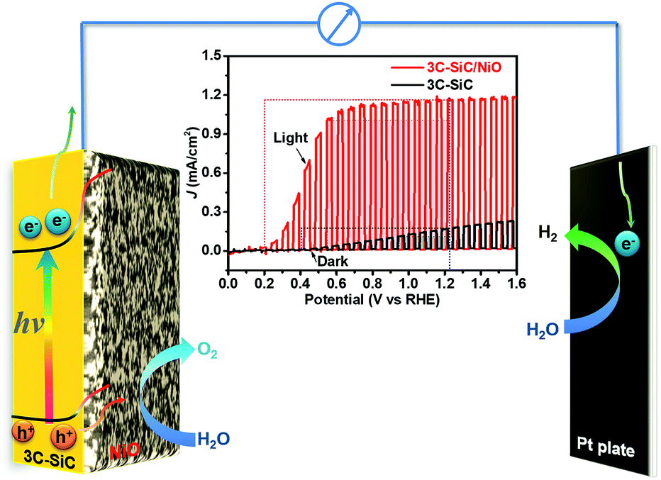 | ||
| Scheme 1 Schematic diagram of the NiO-coated 3C-SiC photoanode and Pt counter electrode for PEC water splitting. The inset shows the photocurrent density versus potential curves of 3C-SiC and 3C-SiC/NiO photoanodes under AM1.5G 100 mW cm−2 illumination. | ||
Experimental section
High crystalline quality 3C-SiC (∼1 mm thick) layers were grown on 4 degree off-axis 4H-SiC substrates by the sublimation technique.32 Then, 350 μm thick free-standing 3C-SiC samples were made by polishing away the 4H-SiC substrates and the interfacial layer. For comparison, the 350 μm thick 3C-SiC samples were cut into two pieces. One piece was used for preparing the 3C-SiC/NiO sample while the other piece was used as a reference. NiO nanoclusters were deposited on the 3C-SiC surface using a high-vacuum sputtering system, similar to a system used in an earlier study to create Fe nanoparticles.37 In this work, a hollow cathode of Ni was used to sputter material and create a plasma growth regime where the particles nucleate and grow. In order to control the degree of oxidation in the particles, oxygen was introduced into the process at a flow rate of 0.08 sccm. This ensured the synthesis of fully oxidized NiO nanoparticles. Then, the 3C-SiC and 3C-SiC/NiO photoanodes were fabricated by the deposition of 200 nm thick Al ohmic contacts on the backside of the 3C-SiC layer. Finally, the photoanodes were sealed with epoxy resin, so that only the photoanode surface was exposed to solution for light illumination in PEC measurements.PEC experiments were carried out in a typical three-electrode configuration in 1.0 M NaOH solution (pH = 13.6) using a potentiostat/EIS (Princeton Applied Research, VersaSTAT 3). The solution was purged with high purity (99.999%) Ar gas for over 30 min before the PEC measurement. Light of AM1.5G 100 mW cm−2 illumination is generated from an AAA solar simulator (LOT-Quantum Design GmbH) calibrated using a standard single-crystal Si photovoltaic cell. A Pt plate (1 × 1 cm2) and Ag/AgCl (saturated KCl) were used as the counter electrode and the reference electrode, respectively. The j–E measurements were done with a scan rate of 30 mV s−1. The potential measured with respect to Ag/AgCl (VAg/AgCl) was converted to the potential versus reversible hydrogen electrode (VRHE) using the following equation: VRHE = VAg/AgCl + V0 + 0.059 × pH, where V0 is the potential of the Ag/AgCl reference electrode with respect to the standard hydrogen potential. The evolved O2 and H2 gases were measured using a micro gas chromatograph (Agilent Technologies 490 Micro GC) in a two-compartment cell. 1.0 M NaOH solution was used as the electrolyte, which was purged with high purity Ar gas for over 30 minutes before the measurement.
High resolution XRD (HRXRD) measurements were performed using a Philips MRD with Cu Kα1 (λ = 1.54 Å). AFM measurements were carried out in tapping mode using a Veeco Dimension 3100. UV-vis absorption measurement was done with a Perkin Elmer Lambda 950 UV/VIS setup. Scanning electron microscopy (SEM) and energy dispersive X-ray spectroscopy (EDXS) images were collected using a LEO 1550 Gemini instrument with an acceleration voltage of 10 kV, WD of 8.5 mm, and an X-Max silicon drift detector (Oxford instruments). X-ray photoelectron spectroscopy (XPS) spectra were recorded on a Kratos Ultra photoelectron spectrometer equipped with a monochromated Al Kα (1486.6 eV) X-ray source operating at 150 W. The pressure in the analysis chamber was always maintained below 10−7 Pa during the acquisition process. High-resolution spectra of Ni 2p and O 1s core levels were recorded using a pass energy of 20 eV at θ = 0° take-off angle (angle between the specimen surface normal and the detection direction). All spectra were calibrated in energy by setting adventitious carbon C 1s at 284.7 eV (binding energy). In this study, no Ar-etching was carried out before spectra acquisitions. The data were treated with the CasaXPS software, using Shirley backgrounds and a Gaussian–Lorentzian (70–30 ratio) function to account for the different components.
Results and discussion
The surface morphology of 3C-SiC grown by the sublimation technique was characterized by atomic force microscopy (AFM). As seen in Fig. 1A, the surface of 3C-SiC is atomically smooth, illustrating regular steps with a terrace width of ∼50 nm and a step height of ∼1.5 nm. The step height corresponds to six Si–C bilayers of the SiC crystalline structure (one SiC bilayer height is 0.25 nm), namely, the dimension of two-unit cells of 3C-SiC. The terraces are originally determined with the off-orientation angle (4°) of Si-face 4H-SiC substrates. The XRD pattern of 3C-SiC shown in Fig. 1B reveals two sharp diffraction peaks, which are assigned to the (111) and (222) reflections of 3C-SiC, respectively. The HRXRD ω-scan rocking curve of (111) Bragg reflections was measured on the 3C-SiC sample with a foot print of 1 × 2.7 mm2 (see the inset of Fig. 1B). The rocking curve is symmetric with a full width at half-maximum (FWHM) value of 27 arcsec. As a comparison, the commercial hexagonal 4H- and 6H-SiC substrates exhibit a FWHM value of the ω rocking curve in the range of 10–40 arcsec.33 The HRXRD result evidences that our 3C-SiC samples possess a high crystalline quality, which is comparable to the commercial hexagonal SiC (4H- and 6H-SiC). The optical properties of 3C-SiC were characterized using the absorption spectra. As seen in Fig. 1C, 3C-SiC shows a rather sharp band-edge absorption, which indicates a high crystalline quality as confirmed by the HRXRD result. The Tauc plot shown in the inset of Fig. 1C yields an optical bandgap of 2.36 eV, which is consistent with the standard bandgap of 3C-SiC.38 Thus the bandgap of our 3C-SiC samples is favorable for visible sunlight absorption. | ||
| Fig. 1 (A) AFM topography image (5 × 5 μm2) of 350 μm thick free-standing 3C-SiC; (B) XRD pattern of 3C-SiC, the inset shows the HRXRD ω-rocking curve of the 3C-SiC (111) reflection with a FWHM of 27 arcsec. (C) Absorption spectrum and Tauc plot (inset) of 350 μm thick 3C-SiC; (D) top-view SEM image of the 3C-SiC/NiO sample; (E) XRD pattern of the 3C-SiC/NiO sample; (F) absorption spectra of 3C-SiC, 3C-SiC/NiO, ITO substrate, and ITO/NiO samples. The inset shows the Tauc plot of ITO/NiO. | ||
NiO nanoclusters were deposited on 350 μm thick 3C-SiC using a high-vacuum sputter system.37 First, we optimized the thickness of the NiO nanocluster layer by changing the deposition durations from 1 to 8 minutes (see Fig. S1 and S2†) and found that the 3C-SiC sample with NiO deposition for 4 minutes (approximately a 500 nm thick NiO layer was deposited) exhibited the highest photocurrent (see Fig. S3†). Hereafter we shall focus on the 3C-SiC sample with NiO deposition for 4 minutes (denoted as “3C-SiC/NiO” unless stated otherwise). Fig. 1D shows the SEM image of the 3C-SiC/NiO sample. It is seen that a layer of nanoclusters has formed on the surface of 3C-SiC (see also the SEM images of 3C-SiC before and after NiO deposition in Fig. S2†). The EDXS analysis verifies that the elemental components of the deposited nanoclusters are only Ni and O (Fig. S2E and F†). Moreover, the XRD pattern of the 3C-SiC/NiO sample shows typical NiO diffraction peaks from the (111), (200), (220) and (311) reflections (Fig. 1E), which confirms that the deposited layer on 3C-SiC is NiO. To evaluate the optical bandgap of NiO, we measured the absorption spectrum of a thick (>1 μm) NiO sample deposited on ITO because the band-edge absorption of NiO deposited on 3C-SiC was not possible to detect due to the saturation of absorbance from the 350 μm thick 3C-SiC layer. As seen in Fig. 1F, NiO shows a bandgap of ∼3.52 eV, which is very close to the reported bandgap of 3.6 eV for a p-type NiO layer.34 This wide bandgap is highly desirable for coating on 3C-SiC due to the optical transparency in the visible sunlight region. As shown in Fig. 1F, the absorption spectrum of the 3C-SiC/NiO sample is identical to that of bare 3C-SiC, indicating the negligible effect of NiO on the visible sunlight absorption.
XPS measurements were performed to determine the surface composition and chemical states of the NiO deposited on 3C-SiC. As shown in Fig. 2A, the Ni 2p spectrum displays two spin–orbit doublets, which are the typical characteristics of the presence of Ni2+ and have been assigned to Ni 2p3/2 (853.6 and 855.5 eV), Ni 2p1/2 (871.4 and 873.3 eV), and their satellites peaks.39 The fitting peak at 853.6 eV (NiA) is ascribed to the Ni with local screening from the lattice oxygen adjacent to the Ni 2p core hole, and the fitting peak at 855.5 eV (NiB) is attributed to the nonlocal screening Ni or the contribution from Ni surface states.39,40 The O 1s spectrum shown in Fig. 2B exhibits two peaks at 529.5 and 532.1 eV, which have been attributed to the lattice oxygen and the surface adsorbed hydroxyl groups, respectively.39 It is noted that both the Ni 2p and O 1s spectra presented here are identical to the reported XPS results of bulk crystalline and nano-scaled stoichiometric NiO,39 which further confirms that the deposited layer on 3C-SiC is NiO.
 | ||
| Fig. 2 XPS spectra of the Ni 2p region (A) and the O 1s region (B) for the 3C-SiC/NiO sample. | ||
The PEC water splitting measurements were carried out using the 3C-SiC and 3C-SiC/NiO samples as photoanodes in a three-electrode system containing a Pt counter electrode and a Ag/AgCl reference electrode. As shown in Fig. 3A, under chopped 100 mW cm−2 AM1.5G illumination, the 3C-SiC/NiO photoanode exhibits a high photocurrent density (jph) of 1.01 mA cm−2 at a low potential of 0.55 VRHE. This photocurrent density is 33.6 times higher than that of the bare 3C-SiC photoanode (0.03 mA cm−2 at 0.55 VRHE). Notably, the 3C-SiC/NiO photoanode shows a much steeper increase of photocurrent, which almost reaches a plateau value at a very low potential of 0.55 VRHE. Meanwhile, the onset potential (Eonset) is negatively shifted from 0.40 VRHE for the 3C-SiC photoanode to 0.20 VRHE for the 3C-SiC/NiO photoanode (Fig. 3A). This negative shift of the Eonset indicates that the overpotential of water oxidation is significantly reduced.41
 | ||
| Fig. 3 Current density–potential (j–E) curves (A) and ABPE (B) of the 3C-SiC and 3C-SiC/NiO photoanodes in 1.0 M NaOH solution under chopped AM1.5G 100 mW cm−2 illumination, at a scan rate of 30 mV s−1. The photocurrent densities (C) and the evolved H2 and O2 gases (D) of the 3C-SiC and 3C-SiC/NiO photoanodes at 1.0 VRHE under steady-state AM1.5G 100 mW cm−2 illumination in 1.0 M NaOH solution. The dotted lines in (D) represent the theoretical volumes of H2 and O2 with 100% faradaic efficiency, respectively. | ||
Another key parameter for the quantitative measurement of a PEC cell's power characteristics is the “fill factor” (ff), which is given by the equation42,43 ff = jmp × Vmp/[jsc × (1.23 − Eonset)], where jmp and Vmp are the current density and potential at the maximum power point, jsc is the photocurrent density at 1.23 VRHE and Eonset is the onset potential. As seen in Fig. 3A, the 3C-SiC/NiO photoanode exhibits a higher fill factor (57%) than the 3C-SiC photoanode (24%).
Fig. 3B depicts the ABPE curves for both 3C-SiC and 3C-SiC/NiO photoanodes. The ABPE is calculated by the equation ABPE = jph × (1.23 − |Vapp|)/PAM1.5G, where jph is the photocurrent density, Vapp is the applied potential, and PAM1.5G is the light density of simulated sunlight (100 mW cm−2). The 3C-SiC/NiO photoanode demonstrates a maximum ABPE of 0.69% at 0.55 VRHE, which is the highest photoconversion efficiency among those reported for SiC-based photoanodes.44 As a comparison, the 3C-SiC photoanode shows a much lower maximum ABPE of 0.035% at a higher potential of 0.85 VRHE. Notably, the 3C-SiC/NiO heterojunction photoanode not only increases the conversion efficiency but also reduces the required potential to reach the maximum photoconversion efficiency. Moreover, the incident photon-to-current efficiency (IPCE) of the 3C-SiC/NiO photoelectrode is also significantly improved compared to that of the 3C-SiC photoanode (Fig. S4†). The IPCE results show that the photocurrent-response curve is consistent with its absorption spectrum. Under the illumination of 1.0 mW cm−2 410 nm LEDs (spectral line width of 10 nm), the 3C-SiC/NiO photoanode exhibits a high IPCE of 31%.
The PEC water splitting and the measurement of evolved H2 and O2 gases were carried out in a two-compartment cell to separate the H2 and O2 gases. Under steady-state AM1.5G 100 mW cm−2 illumination, the chronoamperometry (j–t) curve of the 3C-SiC/NiO photoanode exhibits a reproducible photocurrent of around 1.0 mA cm−2 at 1.0 VRHE, which is 10 times higher than the photocurrent of the 3C-SiC photoanode (0.1 mA cm−2) under the same conditions (Fig. 3C). Meanwhile, the volumes of O2 and H2 gases were measured by gas chromatography to evaluate the faradaic efficiencies (ηF) of H2 and O2. As shown in Fig. 3D and S5,† the 3C-SiC/NiO photoanode exhibits a higher ηF of ∼80% for O2 production than the 3C-SiC photoanode (∼50% ηF for O2) at a bias of 1.0 VRHE while the ηF for H2 production is close to 100% for both cases. As seen in Fig. S5,† with further increasing the thickness of the NiO layer (>1 μm), a higher O2 evolution efficiency of ∼90% was obtained at 1.0 VRHE but the photocurrent was decreased to 0.5 mA cm−2 at 1.0 VRHE due to the reduced light transmittance (caused by light scattering) through the thicker nanostructured NiO. The improved O2 faradaic efficiencies of the 3C-SiC/NiO photoanodes suggest that NiO can also protect the 3C-SiC surface against photo-corrosion.
As shown in Fig. 3, the 3C-SiC/NiO photoanode clearly demonstrates significant improvements of PEC water splitting performances including enhanced photocurrent and reduced onset potential. For the 3C-SiC photoanode, an onset potential of 0.40 VRHE is substantially anodic of its flat-band potential of −0.22 VRHE, which is determined by Mott–Schottky measurements (see Fig. S6†). This large overpotential of the 3C-SiC photoanode is thought to be caused by the slow kinetics of water oxidation which results in hole accumulation and the subsequent carrier recombination at the photoanode surface.41 However, this sluggish water oxidation issue might be significantly alleviated in the 3C-SiC/NiO photoanode because the NiO deposition on the 3C-SiC surface could form a p–n heterojunction that would promote the separation of the photogenerated electron–hole pairs and thus suppress carrier recombination. This explains the dramatic shift of the onset potential and the significant increase of the photocurrent in the 3C-SiC/NiO photoanode.
To understand the enhanced PEC performance of the 3C-SiC/NiO photoelectrode, we performed photovoltage measurements under open circuit conditions. In the dark, the equilibrium between the photoanode and the electrolyte dictates that the open-circuit potential (OCP) of the photoanode represents the position of the Fermi level. Under illumination, the photogenerated electron–hole pairs are separated by the built-in electric field in the space charge region. The electric field drives the majority carriers into the bulk of the semiconductor and the minority carriers toward the photoanode/electrolyte interface, which would generate a field opposing the built-in electric field in the space charge region. This photogenerated potential results in a negative shift of the measured Fermi level. As seen in Fig. 4A, under AM1.5G 100 mW cm−2 illumination, the open-circuit potentials of the 3C-SiC and 3C-SiC/NiO photoanodes are negatively shifted to 0.51 VRHE and 0.22 VRHE, respectively, which are consistent with their onset potentials shown in Fig. 3A. The difference between the measured OCPs in the dark and under illumination represents a photovoltage (Vph) generated in the photoanode. As seen in Fig. 4A, under AM1.5G 100 mW cm−2 illumination, 3C-SiC exhibits a Vph of 0.7 V and the 3C-SiC/NiO photoanode shows a high Vph of 1.0 V. This photovoltage, to the best of our knowledge, is the highest photovoltage among the reported values for semiconductor photoelectrodes. For instance, recent studies reported a Vph value of 0.45 V for a p-Si/SrTiO3/Ti/Pt photocathode;45 a Vph value of 0.62 V for Fe2O3/NiFeOx photoanodes;46 and a Vph value of 0.41 V for a ZnO/CdSe nanorod photoanode.47
 | ||
| Fig. 4 (A) Open-circuit potentials (OCPs) of the 3C-SiC and 3C-SiC/NiO photoanodes in 1.0 M NaOH under chopped AM1.5G 100 mW cm−2 illumination. The fitting lifetimes indicate the OCP decay times of 3C-SiC and 3C-SiC/NiO after turning off the light. (B) XPS valence band spectra of 3C-SiC and 3C-SiC/NiO. The obtained valence band (EVB) positions are 2.15 eV for 3C-SiC and 1.33 eV for NiO deposited on 3C-SiC with respect to the Fermi energy (EF = 0 eV), respectively. (C) The schematic band positions of the 3C-SiC/NiO heterojunction structure according to the EVB calculated from (B). | ||
The larger photovoltage of the 3C-SiC/NiO photoanode is consistent with the results of the enhanced photocurrent and reduced onset potential. In principle, the separation of the photogenerated carriers ultimately determines the photovoltage, photocurrent, and power characteristics of a PEC water splitting cell. Thus, these enhanced PEC factors of the 3C-SiC/NiO photoanode are caused by the presence of the 3C-SiC/NiO p–n heterojunction that promotes the charge separation and thus reduces the carrier recombination. This is supported by the measurement of the OCP decay time after turning off the light. As seen in Fig. 4A, the OCP decay time (42.9 s) of the 3C-SiC/NiO photoanode is 7 times longer than the decay time (6.0 s) of the 3C-SiC photoanode. The slower OCP decay time in the 3C-SiC/NiO heterojunction photoanode indicates a longer carrier lifetime,48 which suggests that the carrier recombination might be significantly suppressed in the 3C-SiC/NiO photoanode and thus more carriers can reach the photoanode/electrolyte interface to contribute to PEC water splitting.
To confirm the formation of the 3C-SiC/NiO p–n heterojunction, we measured the valence band positions of 3C-SiC and NiO on 3C-SiC by XPS. As seen in Fig. 4B, the obtained valence band (EVB) positions are 2.15 eV for 3C-SiC and 1.33 eV for NiO deposited on 3C-SiC with respect to the Fermi energy (EF = 0 eV), respectively. These values agree with the n-type nature of 3C-SiC and p-type nature of NiO.49Fig. 4C illustrates the schematic band structure of the 3C-SiC/NiO p–n heterojunction according to the obtained EVB positions. Clearly, under light illumination, the built-in electric field in the 3C-SiC/NiO p–n heterojunction would sweep photogenerated electrons into the bulk of 3C-SiC and holes toward NiO, thus enhancing the carrier separation.
To further understand the carrier transport properties across the photoanode/electrolyte interface, electrochemical impedance spectroscopy (EIS) measurements were performed in the frequency range of 10–105 Hz under open-circuit conditions. Fig. 5A and B show the Nyquist plots of the 3C-SiC and 3C-SiC/NiO photoanodes in the dark and under AM1.5G 100 mW cm−2 illumination, respectively. The EIS data are fitted using the equivalent circuits shown in the insets of Fig. 5A and B. As the photoelectrode/electrolyte systems exhibit phase angles lower than −90° in the Bode phase plots (Fig. S7†), which is typically ascribed to the non-ideal capacitive behavior, the constant phase elements (CPE) are used instead of the standard capacitance (C) in equivalent circuits.50 Under dark conditions, an equivalent circuit consists of series resistance (Rs), charge-transfer resistance (Rct) from the semiconductor bulk to its surface, and the constant phase element of the space-charge capacitance (CPESC). It is known that the diameters of the semicircles in the Nyquist plots represent the Rct of the photoanode. As depicted in Fig. 5A, the 3C-SiC/NiO photoanode exhibits a smaller semicircle (lower Rct) than the 3C-SiC photoanode. The fitted values of Rct for the 3C-SiC and 3C-SiC/NiO photoanodes are 1300 and 880 Ω cm2 (Table S1†), respectively. This clearly demonstrates that the 3C-SiC/NiO heterojunction structure significantly reduces the resistance for charge-transfer at the electrode/electrolyte interface.
 | ||
| Fig. 5 Nyquist plots of the 3C-SiC and 3C-SiC/NiO photoanodes under open-circuit conditions in the dark (A) and under AM1.5G 100 mW cm−2 illumination (B). The X- and Y-axes represent the real part (Zre) and the imaginary part (Zim) of the impedance, respectively. The insets show the equivalent circuits used to fit the impedance data of 3C-SiC and 3C-SiC/NiO. | ||
Under AM1.5G 100 mW cm−2 illumination, two-semicircle features are apparent in the Nyquist plot (Fig. 5B). To interpret the EIS data, the charge-transfer resistance from the photoanode to the electrolyte (Rct, trap) and the corresponding capacitance (CPEtrap) are included in the equivalent circuit.51 Compared to 3C-SiC, 3C-SiC/NiO exhibits smaller semicircles, indicating smaller values for both Rct and Rct, trap (see the fitted values in Table S1†). This further confirms that the 3C-SiC/NiO photoelectrode possesses a small charge-transfer resistance from the photoanode to electrolyte for water oxidation.
Conclusions
In summary, we have demonstrated a significantly enhanced PEC water splitting performance using a nanostructured NiO/3C-SiC p–n heterojunction as a photoanode. Under simulated AM1.5G 100 mW cm−2 illumination, the 3C-SiC/NiO photoanode exhibits a high photovoltage of 1.0 V, a photocurrent density of 1.01 mA cm−2 at 0.55 VRHE, a high fill factor of 0.57%, and a very low onset potential of 0.20 VRHE. The faradaic efficiency measurements show that NiO also protects the 3C-SiC surface against photo-corrosion. The valence band positions of 3C-SiC and NiO on 3C-SiC measured by XPS evidence the formation of the 3C-SiC/NiO p–n heterojunction, which promotes the separation of the photogenerated carriers and suppresses the carrier recombination. The EIS measurements confirm that the 3C-SiC/NiO photoanode facilitates the charge transfer across the photoanode/electrolyte interface for water oxidation. In this work, by combining the unique material properties of both 3C-SiC and NiO, we show a rational design strategy to fabricate a heterojunction photoanode for synergetic enhancement of solar water splitting performance.Conflicts of interest
There are no conflicts to declare.Acknowledgements
This work was supported by The Swedish Research Council (Vetenskapsrådet, Grant No. 621-2014-5461; 2018-04670; 621-2014-5825), The Swedish Research Council for Environment, Agricultural Sciences and Spatial Planning (FORMAS, Grant No. 2016-00559), The Swedish Foundation for International Cooperation in Research and Higher Education (STINT, Grant No. CH2016-6722), The ÅForsk Foundation (Grant No. 16-399), and The Stiftelsen Olle Engkvist Byggmästare (Grant No. 189-0243). R. Y. and M. S. acknowledge the financial support of the EU project CHALLENGE. S. E. and U. H. acknowledge the financial support from the Knut and Alice Wallenberg Foundation (KAW 2014.0276) and support from the Swedish Government Strategic Research Area in Materials Science on Functional Materials at Linköping University (Faculty Grant SFO Mat LiU No. 2009 00971).Notes and references
- D. G. Nocera, Acc. Chem. Res., 2012, 45, 767–776 CrossRef CAS PubMed.
- M. Gratzel, Nature, 2001, 414, 338–344 CrossRef CAS PubMed.
- H.-L. Wu, X.-B. Li, C.-H. Tung and L.-Z. Wu, Adv. Sci., 2018, 5, 1700684 CrossRef PubMed.
- B. A. Pinaud, J. D. Benck, L. C. Seitz, A. J. Forman, Z. B. Chen, T. G. Deutsch, B. D. James, K. N. Baum, G. N. Baum, S. Ardo, H. L. Wang, E. Miller and T. F. Jaramillo, Energy Environ. Sci., 2013, 6, 1983–2002 RSC.
- X. Ding, Y. Gao, L. L. Zhang, Z. Yu, J. H. Liu and L. C. Sun, ACS Catal., 2014, 4, 2347–2350 CrossRef CAS.
- Z. B. Chen, H. N. Dinh and E. Miller, Photoelectrochemical Water Splitting: Standards, Experimental Methods, and Protocols, Springer, New York, 2013 Search PubMed.
- I. A. Digdaya, L. Han, T. W. F. Buijs, M. Zeman, B. Dam, A. H. M. Smets and W. A. Smith, Energy Environ. Sci., 2015, 8, 1585–1593 RSC.
- H. B. Yang, J. Miao, S.-F. Hung, F. Huo, H. M. Chen and B. Liu, ACS Nano, 2014, 8, 10403–10413 CrossRef CAS.
- X.-B. Li, C.-H. Tung and L.-Z. Wu, Nat. Rev. Chem., 2018, 2, 160–173 CrossRef CAS.
- A. Fujishima and K. Honda, Nature, 1972, 238, 37–38 CrossRef CAS PubMed.
- M. S. Wrighton, A. B. Ellis, P. T. Wolczanski, D. L. Morse, H. B. Abrahamson and D. S. Ginley, J. Am. Chem. Soc., 1976, 98, 2774–2779 CrossRef CAS.
- B. Cole, B. Marsen, E. Miller, Y. F. Yan, B. To, K. Jones and M. Al-Jassim, J. Phys. Chem. C, 2008, 112, 5213–5220 CrossRef CAS.
- M. Zhou, H. B. Wu, J. Bao, L. Liang, X. W. Lou and Y. Xie, Angew. Chem., Int. Ed., 2013, 52, 8579–8583 CrossRef CAS PubMed.
- T. W. Kim and K. S. Choi, Science, 2014, 343, 990–994 CrossRef CAS PubMed.
- P. Dias, M. Schreier, S. D. Tilley, J. S. Luo, J. Azevedo, L. Andrade, D. Q. Bi, A. Hagfeldt, A. Mendes, M. Gratzel and M. T. Mayer, Adv. Energy Mater., 2015, 5, 1501537 CrossRef.
- J. H. Kim, J. W. Jang, Y. H. Jo, F. F. Abdi, Y. H. Lee, R. van de Krol and J. S. Lee, Nat. Commun., 2016, 7, 13380 CrossRef CAS PubMed.
- P. Xu, J. Y. Feng, T. Fang, X. Zhao, Z. S. Li and Z. G. Zou, RSC Adv., 2016, 6, 9905–9910 RSC.
- Y. W. Liu, L. Liang, C. Xiao, X. M. Hua, Z. Li, B. C. Pan and Y. Xie, Adv. Energy Mater., 2016, 6, 1600437 CrossRef.
- I. Concina, Z. H. Ibupoto and A. Vomiero, Adv. Energy Mater., 2017, 7, 1700706 CrossRef.
- M. D. Hernandez-Alonso, F. Fresno, S. Suarez and J. M. Coronado, Energy Environ. Sci., 2009, 2, 1231–1257 RSC.
- C. X. Guo, Y. Q. Dong, H. B. Yang and C. M. Li, Adv. Energy Mater., 2013, 3, 997–1003 CrossRef CAS.
- J. S. Luo, Z. Li, S. Nishiwaki, M. Schreier, M. T. Mayer, P. Cendula, Y. H. Lee, K. W. Fu, A. Y. Cao, M. K. Nazeeruddin, Y. E. Romanyuk, S. Buecheler, S. D. Tilley, L. H. Wong, A. N. Tiwari and M. Gratzel, Adv. Energy Mater., 2015, 5, 1501520 CrossRef.
- Z. M. Bai, X. Q. Yan, Y. Li, Z. Kang, S. Y. Cao and Y. Zhang, Adv. Energy Mater., 2016, 6, 1501459 CrossRef.
- M. G. Kibria, H. P. T. Nguyen, K. Cui, S. R. Zhao, D. P. Liu, H. Guo, M. L. Trudeau, S. Paradis, A. R. Hakima and Z. T. Mi, ACS Nano, 2013, 7, 7886–7893 CrossRef CAS PubMed.
- T. Yasuda, M. Kato, M. Ichimura and T. Hatayama, Appl. Phys. Lett., 2012, 101, 053902 CrossRef.
- D. H. van Dorp, N. Hijnen, M. Di Vece and J. J. Kelly, Angew. Chem., Int. Ed., 2009, 48, 6085–6088 CrossRef CAS PubMed.
- A. B. Murphy, P. R. F. Barnes, L. K. Randeniya, I. C. Plumb, I. E. Grey, M. D. Horne and J. A. Glasscock, Int. J. Hydrogen Energy, 2006, 31, 1999–2017 CrossRef CAS.
- J. Tae Song, H. Mashiko, M. Kamiya, Y. Nakamine, A. Ohtomo, T. Iwasaki and M. Hatano, Appl. Phys. Lett., 2013, 103, 213901 CrossRef.
- R. S. Pessoa, M. A. Fraga, L. V. Santos, M. Massi and H. S. Maciel, Mater. Sci. Semicond. Process., 2015, 29, 56–68 CrossRef CAS.
- T. Yasuda, M. Kato, M. Ichimura and T. Hatayama, Mater. Sci. Forum, 2013, 740–742, 859–862 Search PubMed.
- N. Ichikawa, M. Kato and M. Ichimura, Appl. Phys. Lett., 2016, 109, 153904 CrossRef.
- V. Jokubavicius, G. R. Yazdi, R. Liljedahl, I. G. Ivanov, R. Yakimova and M. Syväjärvi, Cryst. Growth Des., 2014, 14, 6514–6520 CrossRef CAS.
- J. W. Sun, I. G. Ivanov, R. Liljedahl, R. Yakimova and M. Syväjärvi, Appl. Phys. Lett., 2012, 100, 252101 CrossRef.
- H. Sato, T. Minami, S. Takata and T. Yamada, Thin Solid Films, 1993, 236, 27–31 CrossRef CAS.
- X. H. Zhou, R. Liu, K. Sun, D. Friedrich, M. T. McDowell, F. Yang, S. T. Omelchenko, F. H. Saadi, A. C. Nielander, S. Yalamanchili, K. M. Papadantonakis, B. S. Brunschwig and N. S. Lewis, Energy Environ. Sci., 2015, 8, 2644–2649 RSC.
- K. Sun, Y. Kuang, E. Verlage, B. S. Brunschwig, C. W. Tu and N. S. Lewis, Adv. Energy Mater., 2015, 5, 1402276 CrossRef.
- S. Ekeroth, E. P. Münger, R. Boyd, J. Ekspong, T. Wågberg, L. Edman, N. Brenning and U. Helmersson, Nano Lett., 2018, 18, 3132–3137 CrossRef CAS PubMed.
- M. E. Levinshtein, S. L. Rumyantsev and M. Shur, Properties of advanced semiconductor materials: GaN, AlN, InN, BN, SiC, SiGe, Wiley, New York, 2001 Search PubMed.
- M. A. Peck and M. A. Langell, Chem. Mater., 2012, 24, 4483–4490 CrossRef CAS.
- J. Keraudy, A. Ferrec, M. Richard-Plouet, J. Hamon, A. Goullet and P.-Y. Jouan, Appl. Phys. Lett., 2017, 409, 77–84 CAS.
- S. D. Tilley, M. Cornuz, K. Sivula and M. Gratzel, Angew. Chem., Int. Ed., 2010, 49, 6405–6408 CrossRef CAS PubMed.
- M. G. Walter, E. L. Warren, J. R. McKone, S. W. Boettcher, Q. X. Mi, E. A. Santori and N. S. Lewis, Chem. Rev., 2010, 110, 6446–6473 CrossRef CAS PubMed.
- S. W. Boettcher, E. L. Warren, M. C. Putnam, E. A. Santori, D. Turner-Evans, M. D. Kelzenberg, M. G. Walter, J. R. McKone, B. S. Brunschwig, H. A. Atwater and N. S. Lewis, J. Am. Chem. Soc., 2011, 133, 1216–1219 CrossRef CAS PubMed.
- W. S. Dos Santos, M. Rodriguez, J. M. O. Khoury, L. A. Nascimento, R. J. P. Ribeiro, J. P. Mesquita, A. C. Silva, F. G. E. Nogueira and M. C. Pereira, ChemSusChem, 2018, 11, 589–597 CrossRef CAS PubMed.
- L. Ji, M. D. McDaniel, S. Wang, A. B. Posadas, X. Li, H. Huang, J. C. Lee, A. A. Demkov, A. J. Bard, J. G. Ekerdt and E. T. Yu, Nat. Nanotechnol., 2015, 10, 84–90 CrossRef CAS PubMed.
- C. Du, X. Yang, M. T. Mayer, H. Hoyt, J. Xie, G. McMahon, G. Bischoping and D. Wang, Angew. Chem., Int. Ed., 2013, 52, 12692–12695 CrossRef CAS PubMed.
- J. Miao, H. B. Yang, S. Y. Khoo and B. Liu, Nanoscale, 2013, 5, 11118–11124 RSC.
- Z. H. Zhang and P. Wang, Energy Environ. Sci., 2012, 5, 6506–6512 RSC.
- J. Keraudy, B. Delfour-Peyrethon, A. Ferrec, J. Garcia Molleja, M. Richard-Plouet, C. Payen, J. Hamon, B. Corraze, A. Goullet and P.-Y. Jouan, J. Appl. Phys., 2017, 121, 171916 CrossRef.
- I. A. Digdaya, P. P. Rodriguez, M. Ma, G. W. P. Adhyaksa, E. C. Garnett, A. H. M. Smets and W. A. Smith, J. Mater. Chem. A, 2016, 4, 6842–6852 RSC.
- B. Klahr, S. Gimenez, F. Fabregat-Santiago, J. Bisquert and T. W. Hamann, J. Am. Chem. Soc., 2012, 134, 16693–16700 CrossRef CAS PubMed.
Footnote |
| † Electronic supplementary information (ESI) available. See DOI: 10.1039/c9ta00020h |
| This journal is © The Royal Society of Chemistry 2019 |