
 Open Access Article
 This Open Access Article is licensed under a
 Creative Commons Attribution 3.0 Unported Licence
Deposition and application of a Mo–N back contact diffusion barrier yielding a 12.0% efficiency solution-processed CIGS solar cell using an amine–thiol solvent system
Soňa
Uličná
 *a,
Panagiota
Arnou
b,
Ali
Abbas
a,
Mustafa
Togay
a,
Liam M.
Welch
a,
Martin
Bliss
a,
Andrei V.
Malkov
c,
John M.
Walls
a and
Jake W.
Bowers
*a
*a,
Panagiota
Arnou
b,
Ali
Abbas
a,
Mustafa
Togay
a,
Liam M.
Welch
a,
Martin
Bliss
a,
Andrei V.
Malkov
c,
John M.
Walls
a and
Jake W.
Bowers
*a
aCREST, Wolfson School of Mechanical, Electrical and Manufacturing Engineering, Loughborough University, Loughborough, Leicestershire LE11 3TU, UK. E-mail: s.ulicna@lboro.ac.uk; j.w.bowers@lboro.ac.uk
bPhysics and Materials Science Research Unit, University of Luxembourg, 4422 Belvaux, Luxembourg
cDepartment of Chemistry, School of Science, Loughborough University, Loughborough, Leicestershire LE11 3TU, UK
First published on 7th March 2019
Abstract
Delamination and high series resistance due to excessively thick MoSe2 are commonly found in solution-processed CIGS solar cells. This work shows the effective functionality of Mo–N as a back contact barrier against selenium diffusion during high temperature selenization. Mo–N barrier layers are deposited by reactive D.C. magnetron sputtering. The Mo–N barrier layer significantly reduces MoSe2 formation at the Mo/CIGS interface and consequently improves adhesion properties and enhances crystallinity of the CIGS absorber. The power conversion efficiency (PCE) of a spray-coated diamine–dithiol based CIGS solar cell improved from our previously published 9.8% to 12.0% after application of the Mo–N back contact barrier layer.
1. Introduction
Chalcopyrite Cu(In,Ga)Se2 (CIGS) solar cells are today a well-established and robust thin film photovoltaic (PV) technology with laboratory-level efficiencies exceeding 22%.1 Moreover, CIGS modules with stable power output are commercially available. These highly efficient solar cells and modules are produced using expensive vacuum technologies requiring high capital cost investment as well as high energy and material consumption. Solution-processing of CIGS thin films is a promising alternative to vacuum-based methods, offering a low-cost, large-scale fabrication process via simple deposition techniques such as spray-coating or doctor blading.2,3 However the power conversion efficiencies (PCEs) of solution-processed CIGS solar cells still lag behind that of co-evaporated devices due to the inferior material quality of the CIGS absorber and its interfaces. The Mo/CIGS interface is often of poor quality due to excessive MoSe2 formation when a two-step process (CIGS deposition and selenization) is used.4,5 The presence of a thin MoSe2 interface layer is believed to be beneficial for CIGS device performance creating an ohmic contact between CIGS and Mo.6,7 However, too thick MoSe2 layers often cause adhesion problems and increased series resistance (RS), hence reducing the overall device performance.5,8Various back contact diffusion barriers, including metal oxides and nitrides have been studied in order to prevent Se diffusion to the back contact of the CIGS/CZTS solar cell. These include ZnO, Ag, TiN, TiB4, Mo–N and MoO2.9–16 Suitable barrier layer candidates in addition to preventing Se diffusion should also be sufficiently conductive to allow low resistivity back contacts and be mechanically and chemically stable. Among previously studied layers, ZnO and Ag could diffuse to the absorber and have secondary effects.9–11 TiN is stable but its deposition would require an additional step and material cost.11,12 MoO2 and Mo–N have the advantage of deposition using the same sputtering chamber and Mo target as for Mo deposition, with simply tuning the sputtering gas ratio. It was suggested however, that Mo oxides might also act as diffusion barrier for alkali metals diffusing from soda-lime glass (SLG).13 Mo/MoNx/Mo multilayers employed by Jeon et al. were shown to effectively control the MoSe2 thickness.15 However, resulting CZTS devices had significantly lower performance than devices without the barrier layer, presenting a roll-over behaviour in the current density–voltage (J–V) curve.16
Poor solution-processed CIGS absorber quality generally results from residual impurities in the film after incomplete solvent evaporation. Other drawbacks include composition non-uniformity due to migration of elements upon annealing or difficulty of incorporating selenium into the system resulting in incomplete crystallization.3 The most successful solution-based method was developed by IBM T. J. Watson Research Center and further improved by Zhang et al. achieving 15.2% and 17.3% solution-processed CIGS solar cell respectively.17,18 The process employed is named ‘dimensional reduction’ applying hydrazine as solvent to overcome the solubility problem of metal chalcogenides, which are normally insoluble in common solvents. Hydrazine is however a hazardous and toxic solvent and therefore the potential for an industrial application of this method is limited. Novel techniques for CIGS fabrication have been developed using safer and benign solvents. A molecular ink route combining DMSO and thiourea to dissolve metal chlorides has resulted in CIGS of 14.7% PCE using an anti-reflection coating.19 Metal salts, when used as a precursor material, can leave undesirable impurities in the film, hindering the device performance. Following the ideology of the IBM method, Brutchey et al. effectively dissolved a series of V2VI3 chalcogenides, using a diamine–dithiol solvent mixture instead of hydrazine.20 Our group employed this solvent mixture to readily dissolve Cu2S, In2S3 as well as Ga/Se precursors. These solutions were used to fabricate CuIn(S,Se)2 (CIS) and Cu(In,Ga)(S,Se)2 (CIGS) thin film solar cells in ambient air conditions with PCEs reaching 8% and 9.8% respectively.21 Among other groups using the same solvent combination, Wu et al. successfully dissolved pure metals (Cu, In, Ga) leading to a 9.5% efficient CIGS solar cell.22 Agrawal et al. used a similar solvent structure, monoamine–dithiol, resulting in a pure selenide 12.2% efficient CIGSe.23 This was achieved in a controlled environment of a nitrogen-filled glovebox and using spin-coating which is a difficult technique to scale and therefore not industrially relevant.
In this work we demonstrate similar efficiencies using a spray-coating, which is a scalable deposition technique, and without the need for an inert atmosphere of a glovebox. The application of the Mo–N back contact barrier layer enabled us to improve our previously published 9.8% CIGS to 12.05%. The device fill factor (FF) was improved as a result of only a thin MoSe2 interface layer and Mo–N allowed for longer selenization times resulting in better absorber crystallinity.
2. Results and discussion
2.1 Mo–N layer deposition optimisation
Mo–N layers were deposited by D.C. sputtering introducing different Ar/N2 gas proportions while keeping the deposition pressure constant at 2.3 mTorr (total gas flow rate of 15 sccm). Subsequently, the pressure was varied by introducing more gas into the chamber (10, 15, 30 and 60 sccm) with fixed Ar/N2 ratio (67% N2). Table 1 summarizes the deposition conditions and properties of Mo–N thin films deposited on SLG substrate with varied Ar/N2 ratio (no. 1–4) and sputtering pressure (no. 5–8).| N2 content% | Dep. pressure mTorr | Flow rate sccm | Sheet resistance Ω sq−1 | |
|---|---|---|---|---|
| 1 | 33 | 2.3 | 15 | 9.2 |
| 2 | 50 | 2.3 | 15 | 8.5 |
| 3 | 67 | 2.3 | 15 | 9.5 |
| 4 | 83 | 2.3 | 15 | 8.9 |
| 5 | 67 | 2.0 | 10 | 7.2 |
| 6 = 3 | 67 | 2.3 | 15 | 9.5 |
| 7 | 67 | 3.6 | 30 | 11 |
| 8 | 67 | 5.7 | 60 | 14 |
For all deposition conditions, the Mo–N and sacrificial Mo layer thickness was approximately 100 nm and 50 nm respectively. Therefore the deposition rate is estimated to be 25 nm min−1. The sheet resistance of the bilayer increased with increased sputtering pressure, while it remained relatively constant with varying nitrogen content of the Mo–N layer. The sheet resistance of the sputtered Mo is highly dependent on the sputtering pressure, as previously observed.24 The increase in sheet resistance with higher sputtering pressure is likely caused by the change in material morphology and density. Typically, larger Mo grains and more porous microstructure are observed when sputtering at higher pressures. On the contrary more dense layers are deposited at low pressures. Densely packed microstructure at low working pressures results from longer free pathway and higher kinetic energy of sputtered Mo particles.25
The chemical bonds formed between Mo and N atoms and the nitrogen content of the film with varied deposition conditions were analysed using X-ray photoelectron spectroscopy (XPS) depth profiles. Fig. 1a and b show at% of N 1s and Mo 3d5 peaks found in the XPS analysis of the Mo–N/Mo bilayers prepared using various N2 contents and gas flow rates. The first ∼400 s of etch time correspond to the Mo layer. Approximately 95% of this layer consists of metallic Mo quantified from the Mo 3d5 double peak found at binding energy of 228.2 eV (main peak). Reaching the Mo–N layer at etch time higher than 400 s, the Mo 3d5 peak shifts from 228.2 eV to slightly higher binding energies. This peak shift is clearly visible on a colour map representing the Mo 3d5 double peak for one of the Mo–N/Mo samples in Fig. 1e. It corresponds to the change in chemical bonding from metallic Mo to a Mo–N phase.
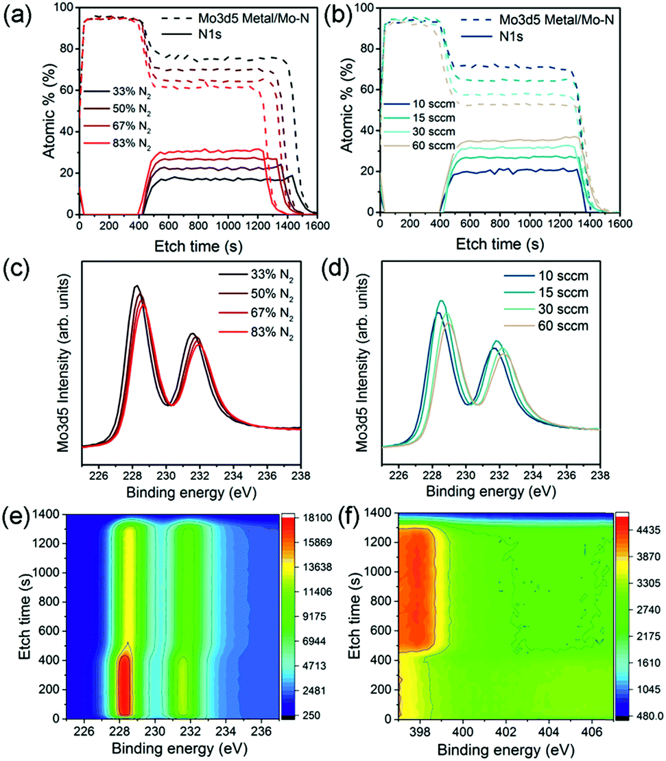 | ||
| Fig. 1 XPS analysis of the Mo–N/Mo depth profile showing at% of Mo and N through the bilayer with Mo–N at varied Ar/N2 ratio at 15 sccm (a) at varied gas flow/pressure with N2 = 67% (b) Mo 3d5 peak at etch time of 990 s for Mo–N films with varied Ar/N2 ratio (c) and at varied gas flow/pressure (d) colour map of Mo 3d5 (e) and N 1s peak (f) at all etching levels for Mo–N at 15 sccm, 67% N2. The colour scale represents peak intensity with arbitrary units. | ||
The N 1s peak was observed at binding energy of 398 eV as shown in Fig. 1f. As expected, with decreased Ar/N2 gas proportions during the deposition, the actual N2 content in the film increased from 17 to 30% (Fig. 1a). Interestingly, with increasing sputtering pressure (by increasing the total gas flow), the N2 content in the Mo–N layer also increased from 20 to 37% (Fig. 1b). At higher pressures more Ar and N ions are available and scattering of sputtered particles increased. Both of these contribute to the formation of a Mo–N film richer in nitrogen. A small, constant amount of oxygen (5 at%) is present throughout the bilayer. It is uncertain whether the oxygen contamination comes from the measurement or deposition.
It can be observed that the etching rate through the Mo–N layer with lower nitrogen content decreased (longer etching time). This can be caused by a slight change in the Mo–N layer thickness or hardness. With high Ar/N2 ratio, more Ar ions are available to bombard the Mo target which would result in a higher deposition rate and thickness of a Mo–N film with low N2 content. Films deposited at lower N2 partial pressures have higher hardness.26 A combination of the thicker films and high hardness for Mo–N with increasing Ar/N2 gas ratio during sputtering would explain the longer XPS etching time seen in Fig. 1a. However, for the films deposited at higher gas flows/pressures, the effects of higher deposition rate and consequently film thickness (from increased sputtering gas ionization), and lower hardness (increase in N2 partial pressure) might compensate each other resulting in similar XPS etch time (Fig. 1b). These small thickness variations could not be detected by the profilometer.
Finally, Fig. 1c and d show the Mo 3d5 peak intensity collected at etch time of 990 s (Mo–N layer) for samples with different N2 content and sputter gas flow/pressure respectively. There is a clear peak shift with varied nitrogen content suggesting a possible change in Mo–N chemical state. In reactive sputtering of Mo–N, different phases including MoN and Mo2N can be observed depending on the sputtering pressure.26 The XPS main Mo 3d5 peak positions together with the X-ray diffraction (XRD) peak positions for all Mo–N films are summarized in Table 2.
| XPS binding energy (eV) | XRD 2θ (°) | |
|---|---|---|
| 1 | 228.3 | 37.7 |
| 2 | 228.5 | 37.3 |
| 3 | 228.6 | 37.1 |
| 4 | 228.7 | 36.8 |
| 5 | 228.4 | 37.1 |
| 6 = 3 | 228.6 | 37.1 |
| 7 | 228.9 | 36.9 |
| 8 | 229.0 | 36.8 |
XRD analysis was performed on all of these samples to investigate changes in crystal structure and chemical bonds of Mo–N phases with the deposition parameters. Fig. 2 shows the XRD patterns of Mo–N/Mo bilayers with varied Ar/N2 gas ratio (top) and gas flow (bottom). The main peak observed at 2θ equal to 40.5° corresponds to the cubic phase of Mo (110) (JCPDS 42-1120). The second most pronounced peak is observed at 2θ ranging from 36.8° to 37.7°. This peak corresponds to the Mo–N phase and its exact position depends on the deposition conditions (Table 2). The peak is shifted to lower diffraction angles with increased sputtering pressure (gas flow) and to higher diffraction angles with increased Ar/N2 ratio. This observation together with the small shift in the Mo 3d5 peak position seen in the XPS (Fig. 1c and d) implies that the crystallographic structure of the Mo–N layer might have been affected by the reactive sputtering conditions. With decreasing Ar/N2 gas proportions during sputtering, the Mo–N becomes richer in N2 and the crystal structure changes from tetragonal Mo2N (112) for N2 = 33% (JCPDS 25-1368) to cubic Mo2N (111) or cubic Mo3N2 (111) for N2 = 50% (JCPDS 25-1366 and 65-4278) to hexagonal MoN (102) for N2 = 83% (JCPDS 74-4266), all performed at 15 sccm. When the gas flow was increased, keeping the N2 content to 67%, the peak shift was smaller. From all the available crystallographic data, these films are closest to the hexagonal MoN phase. XRD analysis confirms the Mo–N phase change with varied N2 content of the film presumed from the XPS analysis and identifies the Mo–N crystallographic structure of each film.
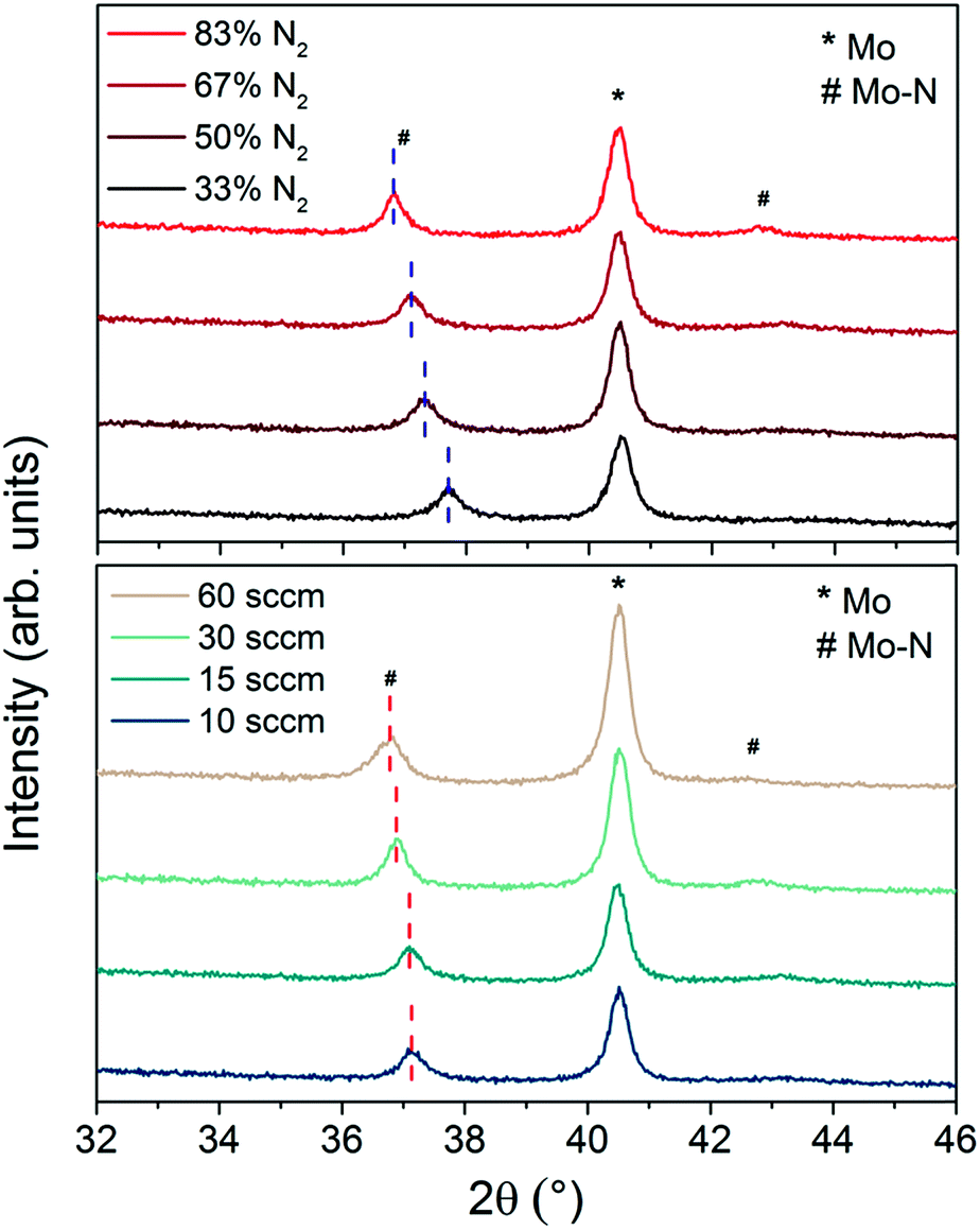 | ||
| Fig. 2 XRD patterns of Mo–N/Mo bilayer with Mo–N deposited with different Ar/N2 ratios at 15 sccm (top) and varied sputtering pressures/gas flows with 67% N2 (bottom). | ||
2.2 Mo–N as a diffusion barrier
In this section, Mo–N/Mo bilayer was deposited onto bare Mo coated SLG using the following conditions: total gas flow of 15 sccm with 67% N2, 2.3 mTorr sputtering pressure. These conditions were chosen based on the analysis above as a compromise between a sufficient film hardness and N2 content. The sheet resistance of the bare Mo measured by four-point probe was found to be 0.28 Ω sq−1 and remained almost unchanged with the introduction of Mo–N/Mo bilayer, 0.27 Ω sq−1.In order to test the barrier layer function as a diffusion barrier against selenium, the stack of Mo/Mo–N/Mo was selenized at 540 °C for 50 min. After selenization, transmission electron microscope (TEM) cross-section of the multilayer was performed and energy dispersive X-ray spectroscopy (EDX) mapping was used to identify the composition of each layer observed. Fig. 3 shows the TEM/EDX analysis of the selenized Mo/Mo–N/Mo multilayer.
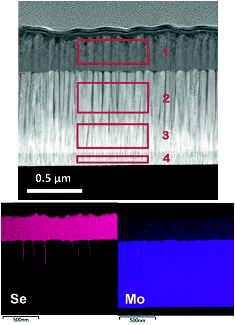 | ||
| Fig. 3 TEM/EDX analysis of selenized Mo/Mo–N/Mo multilayer. Areas 1–4 are quantified in Table 3. | ||
Columnar grains perpendicular to the substrate corresponding to Mo and MoSe2 can be identified. The Mo–N layer is not clearly visible in the high angle annular dark field scanning TEM (HAADF-STEM) image, perhaps due to growing epitaxially onto the Mo layer, as well as little change in Z-contrast and morphology between the layers. Its effect as a diffusion barrier against selenium is evident however. After selenization, almost the entire initial Mo layer stays intact. Some channels along the columnar Mo grains where Se could penetrate under the Mo–N barrier can be observed. Only the top sacrificial Mo, deposited as a Mo–N/Mo bilayer was converted into approximately 340 nm thick MoSe2. The MoSe2 formation is therefore controllable by adjusting the thickness of the sacrificial Mo layer. Table 3 quantifies the composition of 4 areas at different depths through the selenized multilayer using EDX. These areas are indicated by a red rectangle in Fig. 3.
| Mo at% | Se at% | |
|---|---|---|
| Area 1 | 29.7 | 70.3 |
| Area 2 | 98.3 | 1.7 |
| Area 3 | 100 | 0.0 |
| Area 4 | 100 | 0.0 |
The Mo layer was deposited using a typical bilayer approach, including the deposition of a thin adhesive Mo layer at high working pressure followed by a thick, conductive Mo layer at low pressure.24 Area 4 corresponds to the thin, adhesive Mo layer deposited at Ar flow rate of 50 sccm. Areas 2 and 3 belong to the conductive Mo layer deposited at low working pressure achieved with 2 sccm of Ar. Area 1 corresponds to the MoSe2 layer formed on top of the Mo–N barrier. 1.7 at% of Se diffused through the barrier layer into area 2, just below the Mo–N. Hence, the Mo–N effectively worked as a Se diffusion barrier protecting the underlying Mo layer from being converted into MoSe2.
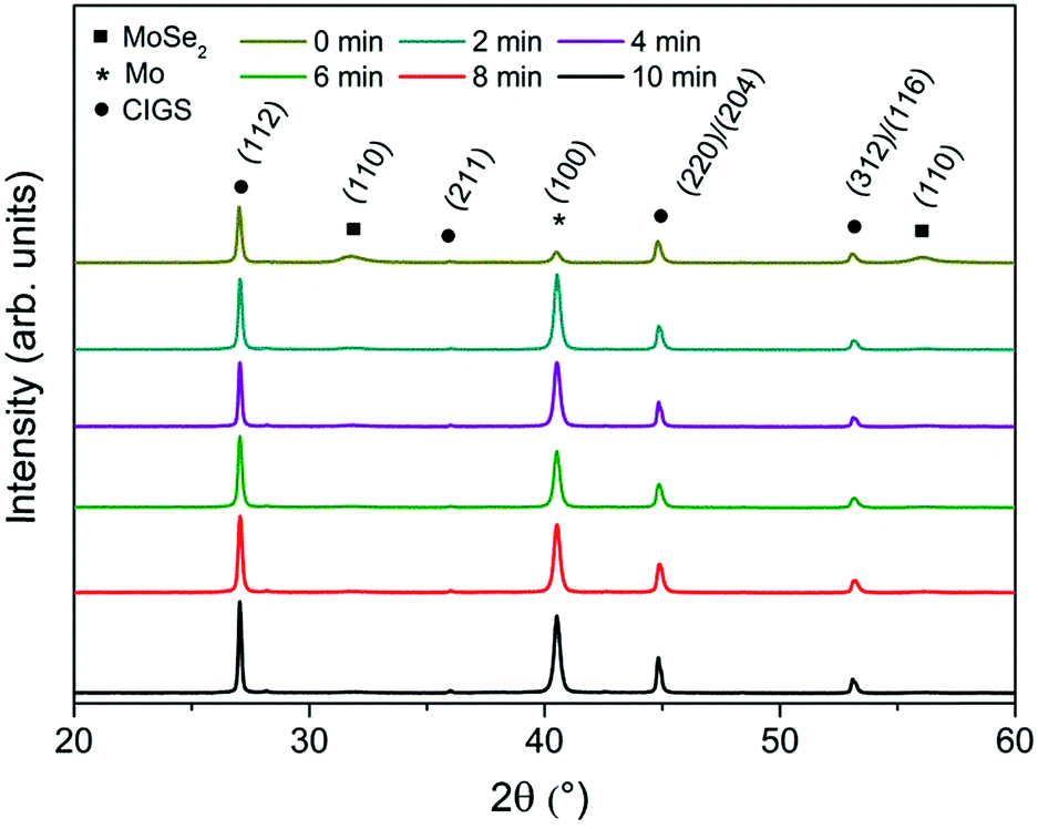
In the following step, the Mo–N barrier layer was applied into complete CIGS devices. The Mo–N barrier layer thickness effect was investigated by varying the deposition time from 2 to 10 min, corresponding to a thickness range of approximately 50–250 nm. Fig. 4 shows the scanning electron microscope (SEM) cross-sections of selenized Mo/Mo–N/Mo/CIGS layers with varied Mo–N layer thickness. It can be observed that performing only 2 min deposition, the Mo–N layer thickness was insufficient to prevent the selenium diffusion completely. Most of the underlying Mo layer was converted into the MoSe2, but no delamination occurred. However, 4 min deposition time (corresponding to ∼100 nm) is already sufficient to provide full coverage of the Mo layer and prevent it from being converted into the MoSe2. Increasing the Mo–N deposition time does not increase the back contact resistivity (back contact sheet resistance remained the same) or affect the absorber crystallization. Fig. 5 shows the XRD patterns of the selenized absorbers on Mo/Mo–N/Mo for varied Mo–N deposition time. A dominant Mo peak is observed at 2θ = 40.5° corresponding to the cubic molybdenum (110) phase (JCPDS 42-1120) and MoSe2 (100) peak at 2θ ∼ 31.8° (JCPDS 29-0914).
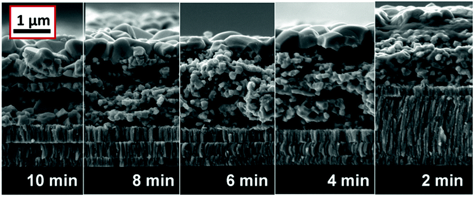 | ||
| Fig. 4 SEM cross-sections of Mo/Mo–N/Mo/CIGS layers after selenization for 90 min. Mo–N layer thickness was varied by varying the deposition time from 10 to 2 min. | ||
 | ||
| Fig. 5 XRD patterns of the Mo/Mo–N/Mo/CIGS films for different Mo–N barrier deposition durations. | ||
Table 4 summarizes the Mo (110)/MoSe2 (100) peak intensity ratio. This ratio increased with increased Mo–N deposition time. The other XRD peaks correspond to the chalcopyrite structure of CuIn0.5Ga0.5Se2 (JCPDS 40-1488). The dominant CIGS (112) peak is found at 2θ ∼ 27.0° and smaller peaks corresponding to (220)/(204) and (312)/(116) planes of tetragonal CIGS phase are found at 2θ ∼ 44.9° and ∼53.1° respectively. The Mo–N peak seen at 2θ ∼ 37.0° in Fig. 2 would overlap with the low intensity CIGS (211) peak.
| Deposition time (min) | Approximate thickness (μm) | Mo/MoSe2 intensity ratio |
|---|---|---|
| 0 | 0 | 1.73 |
| 2 | 0.05 | 55.25 |
| 4 | 0.1 | 64.03 |
| 6 | 0.15 | 70.89 |
| 8 | 0.2 | 76.49 |
| 10 | 0.25 | 126.83 |
Alkali dopants such as Na, were found to promote grain growth of CIGS and CZTS absorber layers.27,28 It is reported that incorporation of Na involves a formation of liquid Na–Se phases during selenization. The reactive selenium provided via Na–Se phases reacts with the metal containing precursors resulting in greatly enhanced grain growth.28 The most common source of Na for CIGS is SLG from which Na migrates to the CIGS absorber during high temperature selenization. However some back contact barrier layers, such as MoO2 can also block Na diffusion from SLG to the absorber.13
In order to study the presence of a small quantity (order of few at%) of light elements (such as Na) in the CIGS absorber, secondary ion mass spectrometry (SIMS) measurement was performed. The two SIMS depth profiles shown in Fig. 6 compare relative quantities of Cu, In, Ga, Se, Mo and Na in CIGS and Mo layers for samples with and without Mo–N barrier layers at the back contact. For this experiment, the Mo–N barrier layer was deposited for 10 min and the absorber was selenized for 90 min. This is an uncalibrated measurement and therefore the data is only relative and not absolute. The inset of Fig. 6 shows the SEM cross-section of the Mo/CIGS layers analysed. From these is clear that rough and porous films were measured resulting in profiles with broader interfaces. Moreover, any partial delamination of the layers in the measurement area would exacerbate this effect and potentially explain the different slope in the Mo signal for both samples.
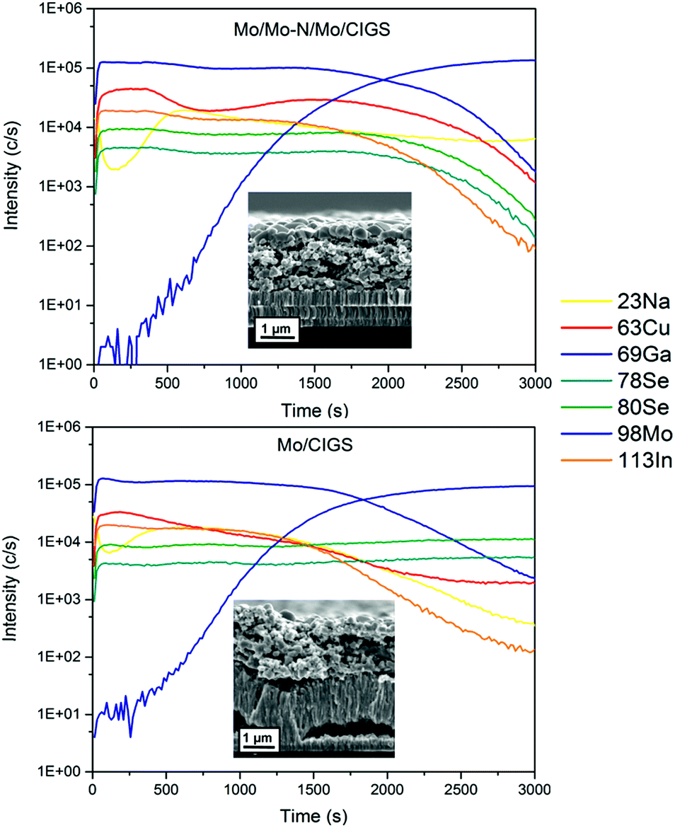 | ||
| Fig. 6 SIMS depth profiles showing the elemental line scans through the absorber deposited on Mo/Mo–N/Mo back contact (top) and on bare Mo (bottom). Inset: SEM cross-sections of the analysed samples. | ||
The profiles of Ga and In are very closely matching within the two samples. The barrier-free sample contains a considerable amount of cracked and partially delaminated MoSe2. Se is present and constant through the absorber and back contact in the barrier-free sample indicating an even distribution of Se through CIGS and MoSe2. The sputtering through the MoSe2 layer was not finished at the end of the 3000 s of analysis time. In comparison, in the Mo–N containing sample Se started to decrease from 2000 s along with In, Ga and Cu profiles implying that the CIGS/Mo interface was reached. Interestingly, in the barrier-free sample, the Cu signal does not decrease along with In and Ga profiles in the MoSe2 layer. The Cu signal is reduced but constantly present in the MoSe2 layer. Copper is a fast diffusing element and has migrated and segregated in the back contact MoSe2 layer, consequently reducing the [Cu]/[Ga + In] (CGI) ratio in the CIGS absorber. Copper diffusion into the MoS2 or MoSe2 has been previously reported in several studies.29–31
High Cu content is essential for good CIGS crystal growth.32 The lower apparent Cu quantity throughout the absorber of the barrier-free sample relative to the barrier-containing sample could cause reduced grain growth and lower short circuit current (JSC). Sodium is present in the bulk of both CIGS absorbers. The surface of the absorber appears to be Na-deficient relative to the bulk however, and similar trend can be observed for both samples. In the barrier-free device, the Na signal shows a smaller local minimum near the surface relative to Na signal in the Mo–N sample. This might be related to the grain size of the crystallised top absorber layer. The grain size is much smaller in the barrier-free absorber. Na is known to passivate grain boundaries (GBs) and there are more GBs present in less crystallised barrier-free absorber surface. Similar SIMS sodium signal shapes are common in the literature.33 SIMS analysis showed that Na diffusion from the SLG was not hindered by the presence of Mo–N barrier layer at the back contact. Moreover, owing to the barrier layer, Cu diffusion from the absorber to the MoSe2 back contact was significantly reduced.
To study the effect of the Mo–N barrier on the device performance, two types of devices were prepared: on a bare Mo-coated substrate and on a Mo/Mo–N/Mo multilayer-coated substrate. Fig. 7 shows a cross-section of CIGS absorbers and back contacts with and without Mo–N barrier (B) after selenization for 50 and 90 min. Without using the barrier layer, over 1 μm thick MoSe2 forms at the Mo/CIGS interface after a 50 min selenization. After a 90 min selenization, the Mo almost completely reacts with Se vapour to form MoSe2 and delamination is observed. Additionally, since more selenium is incorporated into the back contact, the absorber remains poorly crystallized. On the other hand, when a barrier layer acts as Se diffusion barrier, there is more Se available for the absorber recrystallisation. High Cu content and high Se partial pressure are two of the main conditions to achieve a good CIGS crystal growth. Higher Cu content in the absorber on modified Mo/Mo–N/Mo back contact was evidenced by SIMS analysis of the absorbers (Fig. 6). In addition, more Se was available for the whole annealing time to create higher Se partial pressure owing to the lower reaction with Mo to form MoSe2 (Fig. 7). As a result, significantly larger grains are formed at the surface of the absorber, with the largest grains observed after longer selenization.
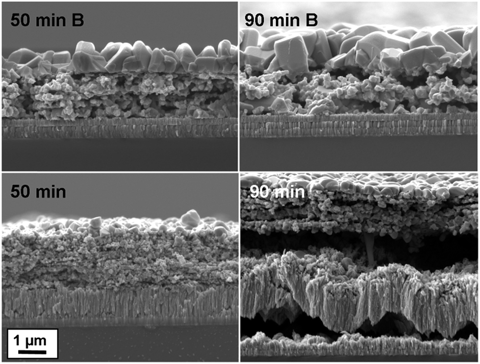 | ||
| Fig. 7 SEM cross-sections through the CIGS absorber and back contact for 50 and 90 min selenized samples with and without Mo–N barrier (B). | ||
The four types of samples were completed into CIGS devices. Fig. 8 shows box plots of PV performance parameters such as open circuit voltage (VOC), JSC, FF and PCE measured on more than 14 cells for each selenization (50 and 90 min) and back contact (B: barrier, or bare Mo) configuration.
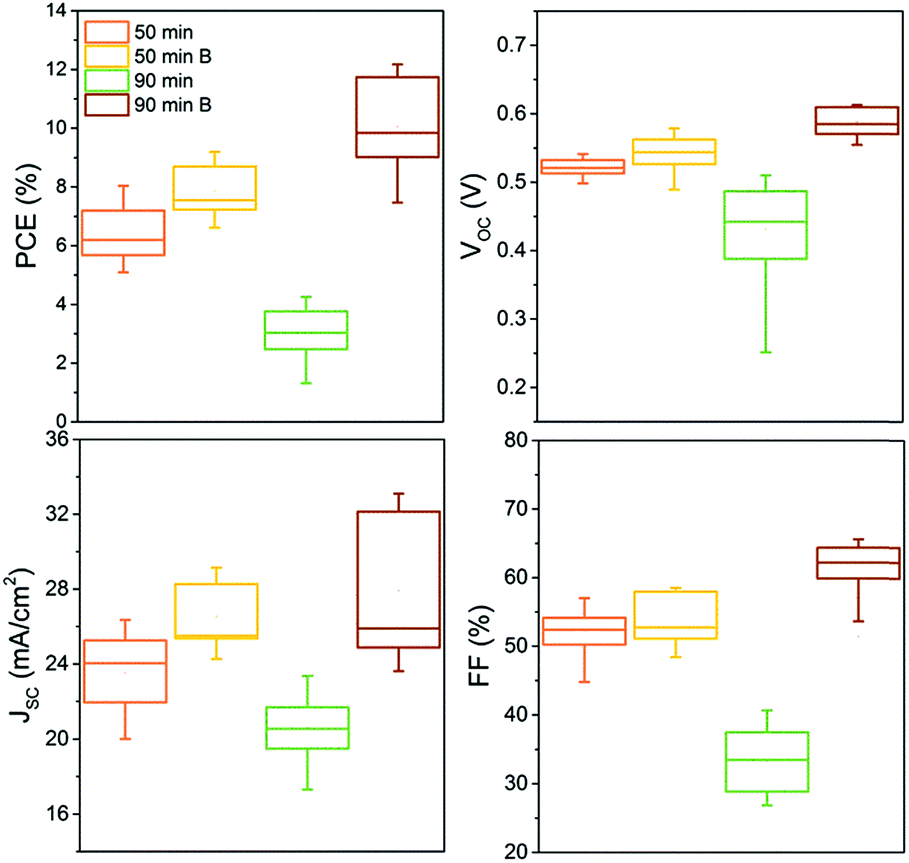 | ||
| Fig. 8 Box plots showing the distribution of PV parameters measured from more than 14 solar cells obtained from minimum two distinct devices for each sample. | ||
As expected from the cross-section SEM image (Fig. 7), the performance of the delaminated (90 min selenized) device on bare Mo is poor with all parameters significantly lower than for the other samples. Its low FF results from the highly resistive and delaminated back contact. Lower JSC and VOC can be attributed to the poor crystallinity of the CIGS absorber containing more grain boundaries. Introducing the back contact barrier (B), the solar cell performance increased from an average 6.5 to 8% with mainly a gain in the short-circuit current density by over 3 mA cm−2 in average after 50 min selenization. A non-negligible gain in VOC is also observed. After a longer (90 min) selenization, the device performance was further increased from an average of 8 to 10%, with an additional gain in VOC (an average of 40 mV) and in FF which increased (in average) from 55 to 63%. The JSC was also increased; however the distribution of the values is much larger implying lateral inhomogeneity of the grain crystallisation. It is anticipated that the improved crystallinity is largely responsible for the remarkable performance improvement. The modified back contact containing only a thin MoSe2 layer likely caused the reduction in the device RS resulting in higher FF, as the MoSe2 is very resistive. The improved device characteristics when the Mo–N barrier was applied, are also reflected in lower diode ideality factor (n) and dark saturation current density (J0). These values along with the typical PV performance parameters are reported in Table 5 for a representative device from each configuration.
| PCE (%) | V OC (V) | J SC (mA cm−2) | FF (%) | R S (Ω cm−2) | R SH (Ω cm−2) | n | J 0 (mA cm−2) | |
|---|---|---|---|---|---|---|---|---|
| 90 min barrier | 12.05 | 0.622 | 28.67 | 67.53 | 0.967 | 331.0 | 1.79 | 3.94 × 10⁻⁵ |
| 50 min barrier | 8.26 | 0.591 | 23.08 | 60.64 | 0.365 | 305.6 | 2.71 | 4.61 × 10⁻³ |
| 50 min | 6.54 | 0.553 | 19.85 | 59.68 | 1.116 | 350.9 | 2.52 | 3.76 × 10⁻³ |
| 90 min | 4.23 | 0.510 | 21.39 | 38.79 | 7.202 | 119.74 | 3.28 | 4.58 × 10⁻² |
2.3 CIGS device with 12% PCE
The Mo–N barrier layer was applied in the back contact of a solution-processed CIGS device. The champion device achieved a PCE of 12.0% (Fig. 9a). This is a significant improvement compared to our previously published CIGS device efficiency (9.8%), which can be attributed to application of the modified back contact Mo/Mo–N/Mo multilayer.21 This allowed for longer selenization durations resulting in improved grain growth without deteriorating the device morphology. We decided to perform further electrical characterisation on our champion solar cell in order to show the improvements relative to our previously published barrier-free CIGS solar cell as well as identify the remaining performance losses. | ||
| Fig. 9 J–V curve (a), EQE spectra (b), doping profile extracted from C–V and DLCP at 300 K (c) and VOCvs. T curve from I–V–T (d). | ||
From Fig. 9b, the external quantum efficiency (EQE) in all wavelengths is relatively high for a solution-processed device, with the maximum value for EQE reached just below 90% at wavelengths between 540 and 570 nm. The strong gradual decay of the EQE for wavelengths > 550 nm seen previously is now visibly attenuated.21 The progressive long wavelength decay is still not completely eliminated because of the presence of the fine-grain layer. It is less pronounced however, as this layer represents a smaller proportion of the final absorber thickness. The absorber bandgap was estimated from the data near the band edge by plotting [E*ln(1 − EQE)]2vs. the photon energy (E) as shown in the inset of Fig. 9b. The band gap estimated from this plot is 1.17 eV. These values are close to the empirical optimum for the CIGS solar cells.34
Capacitance–voltage (C–V) and drive level capacitance profiling (DLCP) measurements at room temperature were performed to estimate the doping density of the absorber. The doping density can be estimated from the local minimum of the U-shaped doping profile obtained from C–V and DLCP measurements.35 The apparent doping density read from the minima of the two curves in Fig. 9c are NC–V ∼ 5.63 × 1016 cm−3 and NDLCP ∼ 5.79 × 1016 cm−3. Both measurements give very similar doping density estimation. Since DLCP is relatively insensitive to the response from interface states and the defects cannot respond effectively to the high excitation frequency used, NDLCP is an indication of free carrier concentration for this study.36
Temperature dependent current–voltage (I–V–T) measurements are useful to determine the dominant recombination path of the CIGS solar cell. By plotting VOCvs. T (Fig. 9d), the activation energy for recombination (EA) can be extracted from the linear extrapolation of the plot to T = 0 K. The activation energy was found to be 1.12 eV. Activation energy equal to the bandgap would indicate that the major recombination mechanism is the Schottky–Read–Hall (SRH) recombination in the bulk, which is the usual mechanism in high-performance CIGS cells.37 However in this case, the EA is slightly lower than the bandgap, which indicates that interface recombination is dominant in the device. Some post deposition treatments such as air annealing of the CIGS/CdS junction was shown to reduce interface recombination by passivating Se vacancies by oxygen atoms.38 The effect of air-annealing on our solution-processed CIGS solar cells was studied elsewhere.39
The electroluminescence (EL) image of the champion cell is displayed in Fig. 10b. The EL shows a spatial inhomogeneity of the cell voltage output under injected current of 5 mA. To find out the origin of this disparity, a TEM cross-section was performed in two distinct points of the cell (Fig. 10a). Image A corresponds to the point A with high EL signal and image B corresponds to point B with less than half of the EL signal of point A. Both cross-sections show significant voids through the absorber depth, which limits the performance in these solution-processed CIGS solar cells and can cause interface problems. Image A shows slightly larger grains and smaller voids than image B, which can explain the better EL signal from this area.
 | ||
| Fig. 10 HAADF-STEM images at two points of the champion CIGS cell (a): A: point of high EL signal, B: point of low EL signal (b). EDX line scan (c) and elemental map (d) through the CIGS champion device in point B. | ||
An EDX line scan and elemental maps were performed through the absorber depth in point B, as shown in Fig. 10c and d. Due to the presence of extensive voids, the CdS grown by chemical bath deposition is enveloping each grain separately and therefore it is present in the bulk of the absorber rather than on the surface only. Ga also segregates occasionally into points of higher concentration located at grain boundaries. The relatively high oxygen concentration observed in the EDX line scan can result from the FIB cross section storage in air between its preparation and the TEM analysis. Therefore this value does not represent the actual content of oxygen in the CIGS absorber. The composition of the CIGS absorber through its depth is relatively constant, with overall [Cu]/[Ga + In] (CGI) and [Ga]/[Ga + In] (GGI) ratios of approximately 0.8 and 0.27 respectively. The CGI found is lower than the intended CGI of 0.9 in the solution, even though Cu is not segregating anymore in the back contact. Cu is a fast migrating element and its high concentration is crucial for a well crystallised CIGS absorber.40 Consequently an investigation of the origin of the Cu deficiency in the absorber and careful adjustment of the CGI ratio will be carried out in the future work.
3. Experimental section
3.1 Mo barrier layer deposition by D.C. magnetron sputtering
Mo–N/Mo bilayers were deposited onto SLG substrates. The deposition was carried out using D.C. magnetron sputtering system at a base pressure lower than 3 × 10⁻⁶ Torr. The Mo target (with an area of 300 cm2) was sputter cleaned for 5 min prior each deposited layer. For the Mo–N barrier layer deposition, a mixture of Ar/N2 sputtering gasses of various proportions (33–83% of N2) and sputter pressures (2.0, 2.3, 3.6 and 5.7 mTorr) were introduced into the sputtering chamber. The deposition was conducted for 4 min using a power density of 4 W cm−2 with the substrate rotating at 3 rpm. A Mo layer with ∼50 nm thickness was deposited on top of the Mo–N layer using 2 sccm of Ar resulting in sputtering pressure of 1.2 mTorr and power density of 4 W cm−2. The top Mo layer is also called ‘sacrificial’ as this Mo layer only will be converted into MoSe2 after selenization. The sheet resistance of the back contact multilayers was measured using a four-point probe. The thickness of each layer was obtained using a profilometer.To study the chemical states of each element present in the sputtered material, XPS depth profiles were performed on bilayers prepared using different deposition conditions. The analysis was carried out using Thermo Scientific K-alpha XPS surface analysis tool with Snapshot acquisition for depth profiling. An electron flood gun was employed to reduce charging to avoid peak shifts. Charge was corrected to the reference C 1s peak at 284.8 eV. A monochromated X-ray Al K alpha source with energy of 1.48 keV and beam width 400 μm was used. During the depth profile acquisition, an Ar+ ion etch at 3 keV, for 30 s at mid current with ion gun raster width of 2.0 mm was performed through the material until the SLG substrate was reached. The chemical states were evaluated by determination of binding energies using curve fitting routines to deconvolute the complex spectra of peaks. A FEI Nova 600 Nanolab dual beam was employed to prepare TEM samples by Focused Ion Beam (FIB) milling. A standard in situ lift out method was used to prepare cross-sectional samples through the coatings into the glass substrate. TEM images were obtained using a FEI Tecnai F20 (S) TEM in the STEM bright field imaging (BF) mode as well as HAADF. The TEM is equipped with an Oxford Instruments X-Max 80 silicon drift detector (SDD) EDX which was used for collecting elemental maps of the PV devices.
3.2 CIGS precursor solution preparation and absorber layer deposition
Individual metal chalcogenide precursor solutions of 0.2 M concentration were prepared by dissolving indium sulphide (In2S3), copper sulphide (Cu2S) and gallium together with selenium powder (Ga + Se) in 1,2-ethylenediamine (EDA)/1,2-ethanedithiol (EDT) solvent mixture of 10/1 v/v ratio. After full precursor dissolution, the separate solutions were combined in specific ratios targeting final composition of Cu0.9In0.7Ga0.3Se2. The final solution was sprayed onto Mo-coated SLG and Mo/Mo–N/Mo multilayer substrates using a chromatography atomizer. The solution preparation and deposition are described in details in our previous work.21 As-deposited CIGS absorbers were subsequently annealed in selenium atmosphere at 540 °C in a closed graphite box containing Se pellets placed inside a tube furnace. The tube was purged with nitrogen several times prior to selenization and the initial pressure was set to 450 Torr. The selenization length was 50 and 90 min including the ramping duration (40 °C min−1). The amount of selenium used was 300 mg for the 50 min anneal and was doubled to 600 mg for the 90 min anneal to supply selenium until the end of the process.The absorber microstructure was studied using a high-resolution field emission scanning electron microscope (FE-SEM) JEOL JSM-7800F operating at 5 kV. XRD data were collected using a Bruker D2 Phaser diffractometer equipped with Lynxeye™ detector and Cu Kα source. The depth profiles of Cu, In, Ga, Se, Na and Mo in the CIGS and Mo layers were examined using SIMS. The analysis was carried out using an O2+ primary ion beam at 10 keV and 150 nA, whilst positive secondary ions were detected. This technique gives a high sensitivity to group 1–13 elements. The measurement was performed at Loughborough Surface Analysis Ltd using the Cameca IMS 3f instrument with 150 μm transfer lens, 175 μm raster size and mass resolution of 300. To eliminate potential charging effects, the samples were coated with a thin layer of gold. No quantification of the data was performed as there was no appropriate reference sample available.
3.3 CIGS solar cell fabrication
CIGS solar cells were completed by depositing approximately 80 nm of CdS by chemical bath from CdSO4, NH4OH and thiourea precursors. This was followed by RF sputtering of intrinsic ZnO and Al doped ZnO (AZO) with a thickness of 80 and 500 nm respectively. Finally 500 nm thick Ag grids were thermally evaporated on the top of the transparent conductive oxide (TCO) using a mask. Cells of an area of 0.25 cm2 were delimited by mechanical scribing.The J–V characteristics were measured using AM1.5G simulated sunlight from a dual source solar simulator (Wacom, Japan) under 100 mW cm−2, calibrated using a Si reference cell. The EQE spectra were obtained at 0 V bias with 5 nm spectral resolution using a Bentham PVE300 system, under ∼0.5 Sun light bias using a halogen source. I–V–T measurement was performed with a Lakeshore 335 temperature controller equipped with a closed cycle helium cryostat (Janis CCS150). Prior to the measurements, the samples were kept in the dark for 1 h to ensure a relaxed state. The temperature was controlled in a range 105–315 K. C–V and DLCP data were acquired using a Keysight E4990A impedance analyser. The voltage was swept from −1 V to 1 V at a frequency of 100 kHz at room temperature. The electroluminescence (EL) images were obtained using an Apogee Alta F800 camera, with a Qioptiq Inspec X IR lens with an aperture f-stop of 2.8. The solar cell was placed under forward bias, with a current injection of 5 mA and images were collected with 10 min acquisition time.
4. Conclusions
In this work we present a hydrazine-free solution-processed CIGS device with 12.0% efficiency using metal chalcogenide precursors and amine–thiol solvents. This considerable improvement in the spray-coated amine–thiol based CIGS solar cell performance was achieved by implementing the Mo–N back contact diffusion barrier. Owing to the modified back contact Mo/Mo–N/Mo multilayer in the CIGS devices, the MoSe2 interface layer thickness was significantly reduced, preventing any delamination even after longer selenization times. FF was improved due to lower series resistance and JSC and VOC increased with improved absorber recrystallisation.The XPS analysis has shown presence of higher nitrogen content in the Mo–N film with reduced Ar/N2 ratio and increased sputtering pressure. The shift in the XRD peak corresponding to Mo–N indicates a phase change from Mo2N to MoN with increased N2 content of the film. As thin as ∼100 nm of Mo–N effectively acts as a diffusion barrier against selenium, preventing conversion of most of the initial Mo layer into resistive MoSe2. SIMS measurements have shown that the Mo–N layer introduced at the back contact did not block the diffusion of sodium from SLG substrate into CIGS absorber. Consequently, a delamination of the CIGS material and copper migration to the back contact were avoided. The barrier layer enabled more Se and Cu available in the absorber to promote the grain growth, resulting in higher EQE signal at longer wavelengths.
Hence, we have shown the relatively simple deposition process and tunability of the Mo–N thin films and its functionality as a diffusion barrier against selenium. Finally, the Mo–N application at the back contact of the CIGS devices allows us to focus on the improvement of the solution-processed absorber without being limited by the back contact resistivity and delamination.
Conflicts of interest
There are no conflicts to declare.Acknowledgements
The authors would like to thank Luke Jones and Dr Patricia Cropper from Loughborough Materials Characterisation Centre (LMCC) for the help with the acquisition and analysis of the XPS depth profiles. Furthermore we would like to acknowledge Dr Ben Grew from Loughborough Surface Analysis Ltd. (LSA) for the SIMS measurement and Alex Smith from CREST Photovoltaic Measurement and Calibration Laboratory for the J–V measurement. The authors would like to acknowledge support from EPSRC (grant no. EP/N026438/1).Notes and references
- NREL, Best Research-Cell Efficiency Chart, https://www.nrel.gov/pv/assets/pdfs/pv-efficiencies-07-17-2018.pdf, accessed November, 2018.
- M. Kaelin, D. Rudmann and A. N. Tiwari, Sol. Energy, 2004, 77, 749 CrossRef CAS.
- T. Todorov and D. B. Mitzi, Eur. J. Inorg. Chem., 2010, 2010, 17 CrossRef.
- T. B. Harvey, I. Mori, C. J. Stolle, T. D. Bogart, D. P. Ostrowski, M. S. Glaz, J. Du, D. R. Pernik, V. A. Akhavan, H. Kesrouani, D. A. Vanden Bout and B. A. Korgel, ACS Appl. Mater. Interfaces, 2013, 5, 9134 CrossRef CAS PubMed.
- S. J. Ahn, K. H. Kim, J. H. Yun and K. H. Yoon, J. Appl. Phys., 2009, 105, 113533 CrossRef.
- D. Abou-Ras, G. Kostorz, D. Bremaud, M. Kalin, F. V. Kurdesau, A. N. Tiwari and M. Dobeli, Thin Solid Films, 2005, 480, 433 CrossRef.
- T. Wada, N. Kohara, S. Nishiwaki and T. Negami, Thin Solid Films, 2001, 387, 118 CrossRef CAS.
- T. Klinkert, B. Theys, G. Patriarche, M. Jubault, F. Donsanti, J.-F. Guillemoles and D. Lincot, J. Chem. Phys., 2016, 145, 154702 CrossRef CAS PubMed.
- W. Li, J. Chen, H. Cui, F. Liu and X. Hao, Mater. Lett., 2014, 130, 87 CrossRef CAS.
- H. Cui, X. Liu, F. Liu, X. Hao, N. Song and C. Yan, Appl. Phys. Lett., 2014, 104, 2 Search PubMed.
- T. Schnabel and E. Ahlswede, Sol. Energy Mater. Sol. Cells, 2017, 159, 290 CrossRef CAS.
- B. Shin, Y. Zhu, N. A. Bojarczuk, S. Jay Chey and S. Guha, Appl. Phys. Lett., 2012, 101, 053903 CrossRef.
- Y. Kamikawa, J. Nishinaga, S. Ishizuka, H. Shibata and S. Niki, Jpn. J. Appl. Phys., 2016, 55, 022304 CrossRef.
- S. Lopez-Marino, M. Espíndola-Rodríguez, Y. Sánchez, X. Alcobé, F. Oliva, H. Xie, M. Neuschitzer, S. Giraldo, M. Placidi, R. Caballero, V. Izquierdo-Roca, A. Pérez-Rodríguez and E. Saucedo, Nano Energy, 2016, 26, 708 CrossRef CAS.
- C.-W. Jeon, T. Cheon, H. Kim, M.-S. Kwon and S.-H. Kim, J. Alloys Compd., 2015, 644, 317 CrossRef CAS.
- J.-Y. Kang, G. Y. Baek, S. Gedi, Y. J. Song and C.-W. Jeon, J. Alloys Compd., 2018, 748, 188 CrossRef CAS.
- T. K. Todorov, O. Gunawan, T. Gokmen and D. B. Mitzi, Prog. Photovoltaics Res. Appl., 2013, 21, 82 CrossRef CAS.
- T. Zhang, Y. Yang, D. Liu, S. C. Tse, W. Cao, Z. Feng, S. Chen and L. Qian, Energy Environ. Sci., 2016, 9, 3674 RSC.
- A. R. Uhl, J. K. Katahara and H. W. Hillhouse, Energy Environ. Sci., 2016, 9, 130 RSC.
- D. H. Webber and R. L. Brutchey, J. Am. Chem. Soc., 2013, 135, 15722 CrossRef CAS PubMed.
- P. Arnou, C. S. Cooper, S. Uličná, A. Abbas, A. Eeles, L. D. Wright, A. V. Malkov, J. M. Walls and J. W. Bowers, Thin Solid Films, 2017, 633, 76 CrossRef CAS.
- D. Zhao, Q. Tian, Z. Zhou, G. Wang, Y. Meng, D. Kou, W. Zhou, D. Pan and S. Wu, J. Mater. Chem. A, 2015, 3, 19263 RSC.
- X. Zhao, M. Lu, M. J. Koeper and R. Agrawal, J. Mater. Chem. A, 2016, 4, 7390 RSC.
- J. H. Scofield, A. Duda, D. Albin, B. L. Ballard and P. K. Predecki, Thin Solid Films, 1995, 260, 26 CrossRef CAS.
- Z.-H. Li, E.-S. Cho and S. J. Kwon, Appl. Surf. Sci., 2011, 257, 9682 CrossRef CAS.
- H. A. Jehn, J.-H. Kim and S. Hofmann, Surf. Coat. Technol., 1988, 36, 715 CrossRef CAS.
- D. Braunger, D. Hariskos, G. Bilger, U. Rau and H. W. Schock, Thin Solid Films, 2000, 361, 161 CrossRef.
- C. M. Sutter-Fella, J. A. Stückelberger, H. Hagendorfer, F. La Mattina, L. Kranz, S. Nishiwaki, A. R. Uhl, Y. E. Romanyuk and A. N. Tiwari, Chem. Mater., 2014, 26, 1420 CrossRef CAS.
- T. Gershon, C. Hamann, M. Hopstaken, Y. S. Lee, B. Shin and R. Haight, Adv. Energy Mater., 2015, 5, 2 Search PubMed.
- B. Shin, O. Gunawan, Y. Zhu, N. A. Bojarczuk, S. Jay Chey and S. Guha, Prog. Photovoltaics Res. Appl., 2013, 21, 72 CrossRef CAS.
- S. Bag, O. Gunawan, T. Gokmen, Y. Zhu, T. K. Todorov and D. B. Mitzi, Energy Environ. Sci., 2012, 5, 7060 RSC.
- S. Nishiwaki, S. Siebentritt, M. Giersig and M. C. Lux-Steiner, J. Appl. Phys., 2003, 94, 6864 CrossRef CAS.
- D. Colombara, U. Berner, A. Ciccioli, J. C. Malaquias, T. Bertram, A. Crossay, M. Schöneich, H. J. Meadows, D. Regesch, S. Delsante, G. Gigli, N. Valle, J. Guillot, B. El Adib, P. Grysan and P. J. Dale, Sci. Rep., 2017, 7, 43266 CrossRef PubMed.
- M. A. Contreras, K. Ramanathan, J. AbuShama, F. Hasoon, D. L. Young, B. Egaas and R. Noufi, Prog. Photovoltaics Res. Appl., 2005, 13, 209 CrossRef CAS.
- J. T. Heath, J. D. Cohen and W. N. Shafarman, J. Appl. Phys., 2004, 95, 1000 CrossRef CAS.
- L. Yin, G. Cheng, Y. Feng, Z. Li, C. Yang and X. Xiao, RSC Adv., 2015, 5, 40369 RSC.
- V. Nadenau, U. Rau, A. Jasenek and H. W. Schock, J. Appl. Phys., 2000, 87, 584 CrossRef CAS.
- U. Rau, D. Braunger, R. Herberholz, H. W. Schock, J.-F. Guillemoles, L. Kronik and D. Cahen, J. Appl. Phys., 1999, 86, 497 CrossRef CAS.
- S. Uličná, M. Togay, M. Bliss, V. Tsai, L. D. Wright, J. Lowe, A. V. Malkov, J. M. Walls and J. W. Bowers, 2018 IEEE 7th WCPEC, Waikoloa Village, HI, 2018, p. 0859 Search PubMed.
- W. Witte, R. Kniese and M. Powalla, Thin Solid Films, 2008, 517, 867 CrossRef CAS.
| This journal is © The Royal Society of Chemistry 2019 |