
 Open Access Article
 This Open Access Article is licensed under a Creative Commons Attribution-Non Commercial 3.0 Unported Licence
A graphene/ZnO electron transfer layer together with perovskite passivation enables highly efficient and stable perovskite solar cells†
Mohammad Mahdi
Tavakoli
 *ab,
Rouhollah
Tavakoli
b,
Pankaj
Yadav
c and
Jing
Kong
*a
*ab,
Rouhollah
Tavakoli
b,
Pankaj
Yadav
c and
Jing
Kong
*a
aDepartment of Electrical Engineering and Computer Science, Massachusetts Institute of Technology, Cambridge, MA 02139, USA. E-mail: mtavakol@mit.edu; jingkong@mit.edu
bDepartment of Materials Science and Engineering, Sharif University of Technology, 14588 Tehran, Iran
cDepartment of Solar Energy, Pandit Deendayal Petroleum University, Gandhinagar-380007, India
First published on 3rd December 2018
Abstract
Interface engineering in organometal halide perovskite solar cells (PSCs) has been an efficient tool to boost the performance and stability of photovoltaic (PV) devices. It is known that zinc oxide (ZnO) is one of the promising electron transporting layers for solar cells and is also applicable for flexible devices. However, the utilization of ZnO in PSCs is restricted due to its reactivity with the perovskite film during the annealing process. Here, we demonstrate improved photovoltaic performance and stability by introducing monolayer graphene (MLG) at the interface of the ZnO ETL and perovskite absorber, which results in a stable electric to power conversion efficiency (PCE) of 19.81%. The device based on this modified ETL maintains more than 80% of its initial PCE value after 300 h under continuous illumination. Interestingly, we find that the presence of MLG at the ETL/perovskite interface not only improves the carrier extraction and photovoltaic properties but also protects the perovskite film from decomposition at elevated temperatures, which is beneficial for the stability of the device. To improve the stability even further, we have passivated the surface of the perovskite film by using a new modulator, i.e., 3-(pentafluorophenyl)-propionamide (PFPA) to abate the surface trap states of the perovskite. Based on our modification with MLG and PFPA, a stable PSC device with a PCE of 21% was achieved under AM 1.5G illumination with negligible hysteresis. The stability result indicates that the passivated device on MLG/ZnO maintains 93% of its initial PCE value after 300 h under continuous illumination.
Introduction
Rapid progress in organohalide metal perovskite solar cells (PSCs) in terms of performance and stability has attracted tremendous attention from many researchers in the field of photovoltaics.1–5 Low-cost processing, ease of fabrication, high carrier mobility and diffusion length, and strong and broad absorption make them ideal candidates for the fabrication of efficient solar cells with a certified PCE of 23.3%.6–11 It was found that controlling the interface of PSCs plays a crucial role in mitigating carrier recombination that could result in higher photovoltaic parameters.12–15 Recently, various types of ETLs, such as TiO2, ZnO, SnO2, PCBM, etc. have been used for the fabrication of efficient PSCs.16–21 Among all alternative ETLs, ZnO is a promising candidate for the fabrication of efficient PSCs due to its higher electron mobility than TiO2 and extraordinary charge extraction properties.22–24 These features could accelerate the transportation of photogenerated electrons, resulting in efficient and hysteresis-free PSC devices. However, ZnO-based PSCs suffer from the unwanted reaction between ZnO and perovskite layers, happening during the annealing of the perovskite at 100 °C.25–30 This issue needs to be addressed for the fabrication of efficient and stable PSCs. In the literature, several strategies have been employed to solve this problem for example, synthesis of a new nanocomposite based on ZnO, applying an interfacial layer as a barrier between ZnO and the perovskite layer, and passivation of the ZnO film. Zhang et al.31 inserted a thin layer of small molecule [6,6]-phenyl-C61-butyric acid methyl ester (PCBM) between ZnO and perovskite to improve the thermal stability of PSCs. They reported a stable PCE of 19.1% based on this modification. Cao et al.32 passivated the surface of the ZnO ETL using MgO for better charge transport, higher PCE and thermal stability together with ethanolamine to eliminate the hysteresis effect. Based on these modifications, they reported a stable and hysteresis-free PSC device with a PCE of 21.1%.In this work, we investigate an alternative interfacial layer, i.e., ZnO/graphene to minimize the reaction of perovskite with the ZnO ETL. We transfer MLG on top of the ZnO ETL to prevent the chemical reaction at the interface between the perovskite absorber layer and ZnO ETL, as schematically shown in Fig. 1. We found that during the annealing process, the perovskite film which is in direct contact with ZnO decomposes into the PbI2 phase partially. This reaction is significantly suppressed by using MLG as an interfacial layer, as shown in Fig. 1b. In addition to the modification of the ETL in a PSC, surface passivation of perovskite films is another strategy to annihilate the surface trap states and modify the interface between the absorber layer and hole transporting layer (HTL). Recently, some research groups have passivated the surface of perovskite films to further mitigate the radiationless carrier recombination, mostly resulting in a higher open circuit photovoltage (Voc) as well as a higher PCE.33–38 Herein, the surface of the perovskite film has been passivated with a thin layer of PFPA modulator (Fig. 1c). Time-resolved photoluminescence (TRPL) results show a strong quenching effect upon these modifications. Finally, the modified device depicts a PCE of 21% which is ∼52% higher than the performance of the reference cell with the ZnO ETL. More interestingly, the optimized device based on MLG/ZnO and perovskite passivation demonstrates excellent operational stability after 300 h under continuous illumination with only 7% PCE loss.
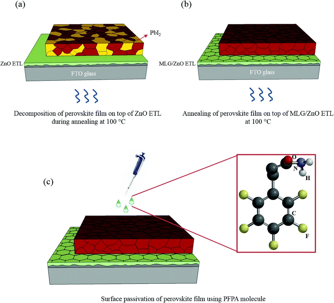 | ||
| Fig. 1 Schematics of perovskite films annealed on top of the (a) ZnO ETL and (b) MLG/ZnO ETL. (c) Surface passivation of the perovskite film using the PFPA modulator. | ||
Results and discussion
The influence of annealing temperature on the perovskite thin film deposited over ZnO was studied by scanning electron microscopy (SEM). Fig. 2a and b show the SEM images of the perovskite film deposited on the ZnO ETL after annealing at 100 °C. As seen, the perovskite film is decomposed in some areas during the annealing process. The inset image in Fig. 2a shows the photograph of the perovskite film annealed on the ZnO ETL at 100 °C. Upon annealing, the color of the perovskite film turned from brownish to yellowish. (More top-view SEM images of the perovskite film annealed on top of the ZnO ETL are shown in Fig. S1†). From the SEM images, it is clear that the perovskite film is decomposed locally and there are many regions with a mixture of PbI2 and perovskite. To check the influence of the annealing temperature, PSC devices with the perovskite absorber layer sandwiched between the ZnO ETL and spiro-OMeTAD as a hole transport layer (HTL) were fabricated and tested. The current–voltage (J–V) curves of the corresponding devices measured under standard illumination of AM 1.5G at 25 °C are shown in Fig. 2c. Here the PCEs of devices fabricated on the ZnO ETL annealed at 70, 85, and 100 °C for 1 h are presented. The increase in annealing temperature yields a gradual decrease in the PCE of the devices, indicating the instability of the double A-cation (FAMA) perovskite film deposited on the ZnO ETL at elevated temperatures. From Fig. 2c, the best result here is seen in the PSC device annealed at 70 °C. The corresponding device illustrates a short circuit current density (Jsc) of 18.3 mA cm−2, an open circuit voltage (Voc) of 0.99 V, a fill factor (FF) of 69% and a PCE of 12.7%. We found that at the annealing temperature of 70 °C, all the photovoltaic parameters are improved drastically as compared with those at higher annealing temperatures, due to the better crystallization of the perovskite absorber layer as supported by the SEM image.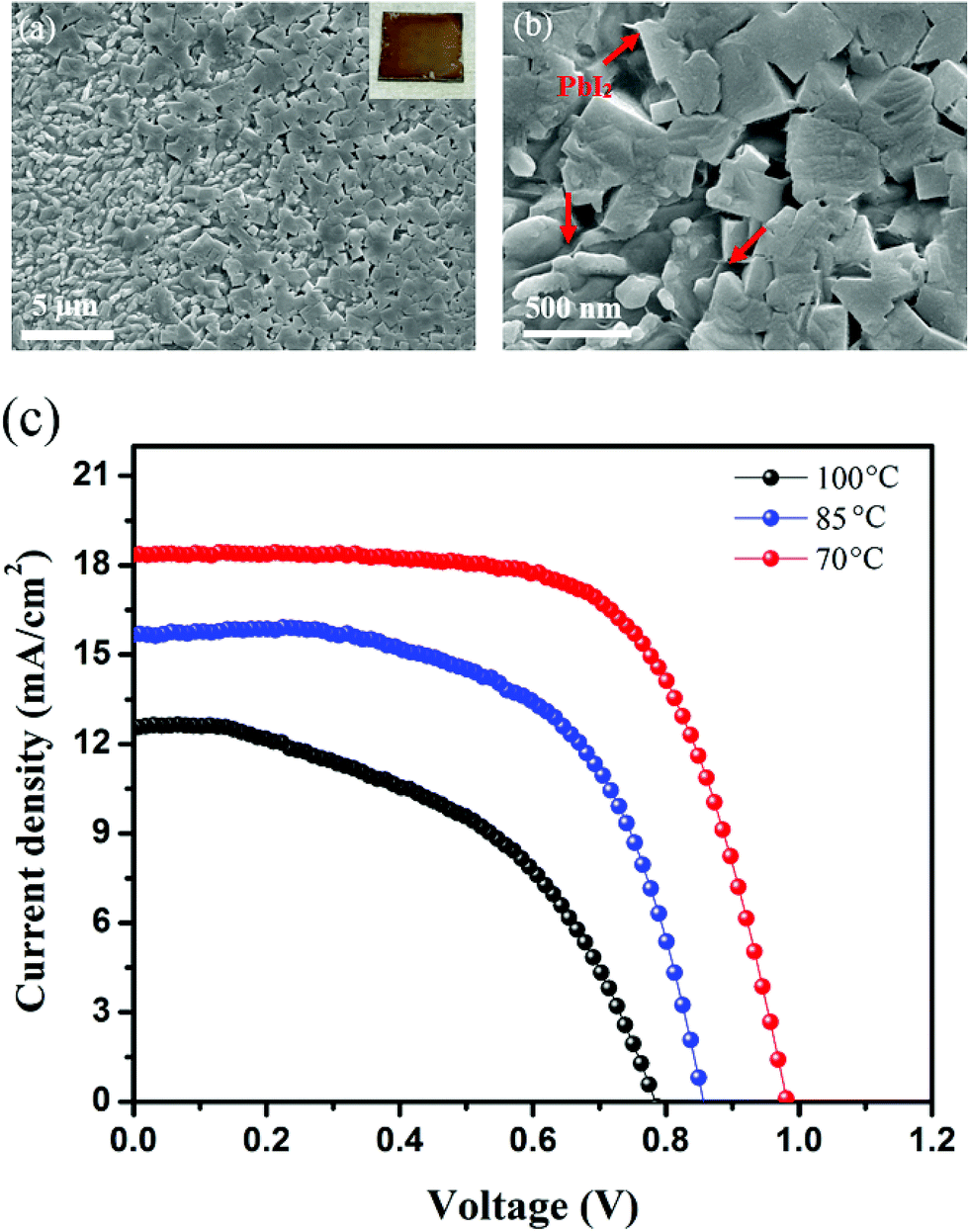 | ||
| Fig. 2 Top view SEM images of the perovskite film annealed at 100 °C for 40 min with low (a) and high (b) magnification indicating the decomposition of perovskite into PbI2 flakes (red arrows show the PbI2 flakes). (c) J–V curves of PSC devices based on the ZnO ETL annealed at 70, 85, and 100 °C. | ||
A key challenge in working with the ZnO ETL in a PSC device is its oxygen containing groups such as the hydroxide group, which can absorb methylammonium iodide (MAI) or formamidinium iodide (FAI) at high temperatures.29 This results in defect formation and perovskite decomposition into the PbI2 phase. To tackle this problem, we have inserted mono layer graphene (MLG) at the interface of perovskite/ZnO. Fig. S2† shows the atomic force microscopy (AFM) images of MLG after transfer onto the surface of the ZnO ETL, indicating the cleanness of this process. The result of surface analysis by AFM shows the formation of a smooth surface for the MLG/ZnO ETL with a roughness of 16 ± 4 nm. After deposition of the perovskite film on the MLG/ZnO ETL, we found that the presence of MLG hinders the decomposition of the perovskite film upon the annealing process. In this work, we fabricate the perovskite film by using a two-step deposition method due to the hydrophobicity issue of MLG. We have used a chlorine-doped perovskite absorber layer in order to improve the crystallinity and enlarge the grain size. The surface morphology of the perovskite absorber layer deposited on MLG/ZnO ETLs (after 150 °C annealing) is shown in Fig. S3†, we found that the perovskite absorber layer is even stable at 150 °C, clearly indicating the role of MLG in the thermal stability and crystallization of the perovskite film. As compared to the perovskite film formed on the bare ZnO ETL (Fig. 2a and b), the perovskite absorber layer on top of MLG/ZnO shows a significant difference in crystallization, with a large grain size of over 1 μm. The difference in grain sizes can be attributed to the differences in annealing temperatures. As shown in Fig. S4,† the perovskite on MLG/ZnO annealed at 150 °C shows much larger grain sizes than the perovskite on ZnO annealed at 70 °C.
Up to now, many fabrication techniques have been reported for the synthesis of the perovskite absorber layer and the final product of these methods results in the formation of polycrystalline perovskite films with many surface defects due to the presence of grain boundaries and ionic vacancies. These defects on the surface of the perovskite film can cause non-radiative recombination which results in shorter diffusion length and lower Voc. Surface engineering of perovskite films using judiciously designed additives is a key solution to mitigate surface defects and facilitate charge transfer properties. So far, different types of passivating modulators such as phenyl-C61-butyric acid methyl ester (PCBM), thiophene, pyridine, and adamantanes have been reported39–41 to remove surface defects e.g. unbonded Pb atoms and iodine vacancies. Here we have applied a PFPA molecule containing fluorine halide on top of the perovskite to annihilate surface defects and studied its optical and photovoltaic properties.
The influence of the improved grain size and better crystallinity on the optoelectronic properties of the perovskite absorber layer on the MLG/ZnO ETL without and with passivation was also analysed by UV-Vis and photoluminescence (PL) measurements. Fig. 3a shows the normalized UV-visible absorption and photoluminescence (PL) spectra of the perovskite absorber layer on ZnO, MLG/ZnO, and the passivated perovskite on MLG/ZnO by PFPA. As seen, no significant change is observed in the band gap (1.57 eV) of the double A-cation perovskite absorber layer. The PL spectra clearly show a strong quenching effect by MLG/ZnO as compared to the ZnO ETL. Upon passivation, this effect is slightly reduced due to the surface modification of the perovskite film. Fig. 3b illustrates the time-resolved PL (TRPL) curves of the corresponding perovskite films. We found that MLG strongly quenches the PL signal as compared to the bare ZnO ETL, indicative of fast charge transport across the interface between the perovskite and MLG/ZnO ETL. Moreover, the TRPL curve of the passivated perovskite film by PFPA shows a slightly weaker quenching effect which may be due to the suppression of the surface trap states of the perovskite film. Fig. 3c and d depict the electron beam-induced current (EBIC) images of PSC devices based on MLG/ZnO without and with PFPA passivation. We performed this measurement to further study the role of PFPA passivation in charge transfer inside the perovskite absorber layer. The voltage and current were fixed to 10 kV and 170 pA, respectively, in this measurement. Fig. S5† shows the EBIC image of devices without and with PFPA passivation extracted from the interface between the perovskite and HTL. The EBIC current was calculated from these images and is shown in the colorful images of Fig. 3c and d. As seen, without PFPA passivation, the EBIC image depicts poor uniformity with a weak signal due to the surface trap states in the perovskite film. This suggests that we have faster carrier recombination in some areas with low intensity. In contrast, the EBIC image of the passivated device shows a much more uniform and stronger signal in all parts of the devices due to the annihilation of surface defects by PFPA (Fig. 3d). This indicates that the carriers in the passivated device can be easily extracted from the perovskite layer with a lower recombination as compared to devices without passivation. These results are in good agreement with the TRPL results as well.
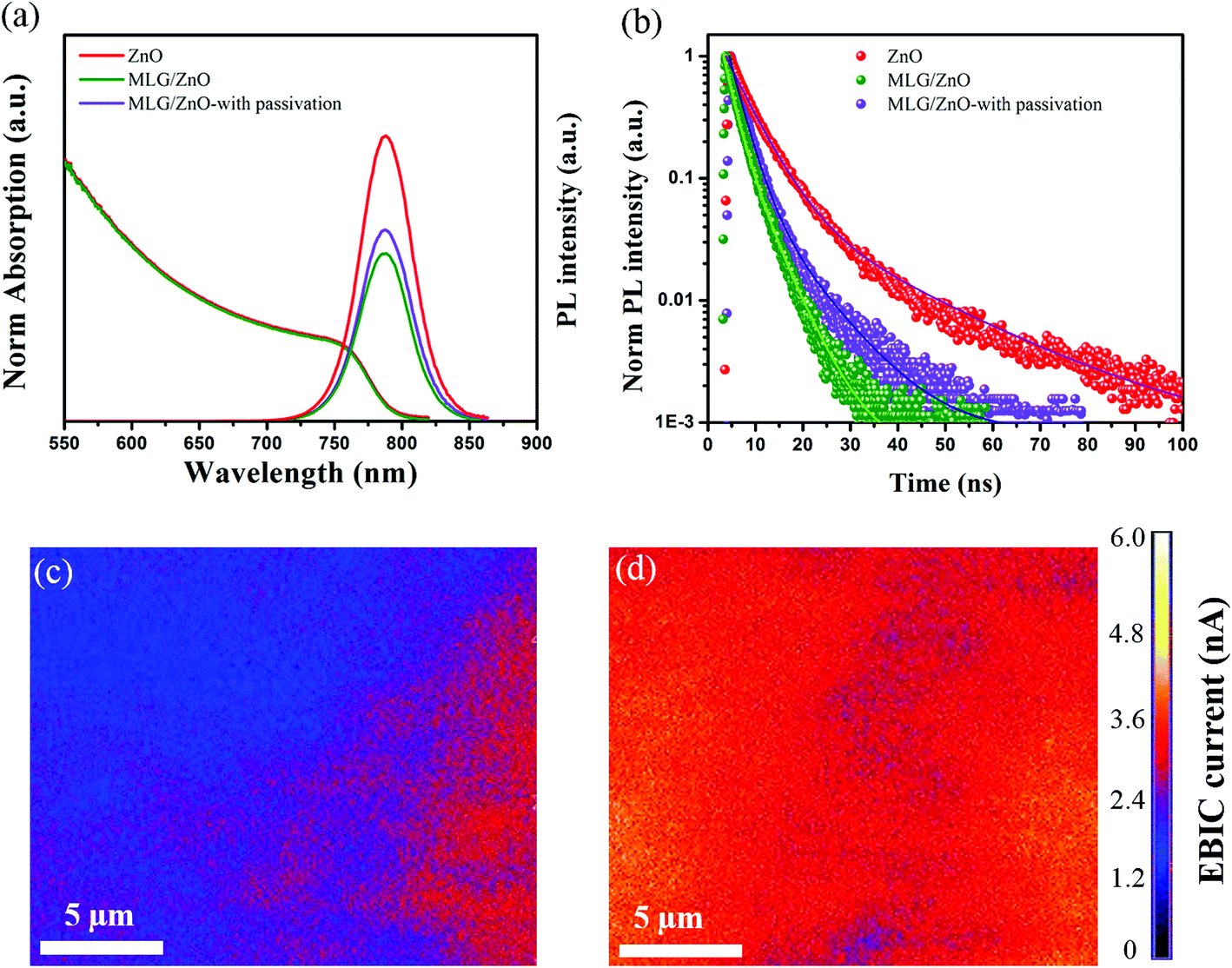 | ||
| Fig. 3 (a) UV-visible absorption and photoluminescence (PL) spectra, and (b) time-resolved PL (TRPL) curves of perovskite films on ZnO, MLG/ZnO, and MLG/ZnO with passivation. Top-view EBIC images of devices based on MLG/ZnO before (c) and after (d) passivation with PFPA. | ||
To further study the role of MLG together with perovskite passivation, PSC devices based on ZnO and MLG/ZnO without and with passivation were fabricated. Fig. 4a shows the cross-sectional SEM image of the device fabricated on MLG/ZnO after passivation of perovskite by PFPA. The fabricated PSCs consist of ZnO-coated FTO glass as the ETL modified by MLG, a 400 nm-thick passivated perovskite absorber, a 150 nm-thick spiro as the HTL, and a gold contact with a thickness of 80 nm. The J–V measurements of the corresponding devices in reverse and forward sweeps with a scan rate of 50 mVs−1 under standard illumination of AM 1.5G (100 mW cm−1) at 25 °C are shown in Fig. 4b. Importantly, the PSCs on MLG/ZnO without and with passivation show a low hysteresis index likely due to the improvement in the ETL and thus efficient carrier extraction. As can be seen in Table 1, the hysteresis index is reduced from 6.4 for the ZnO device to 1.39 and 0.91 for devices on the MLG/ZnO ETL without and with passivation of the perovskite, respectively. Figures of merit for the best performing PSC devices based on ZnO, MLG/ZnO, and MLG/ZnO-with passivation are summarized in Table 1. The ZnO-based PSC depicts the least photovoltaic performance with a Jsc of 20.63 mA cm−2, a Voc of 996 mV, a FF of 67.3%, and a PCE of 13.82% measured under reverse scan. The reason for such low PCE for ZnO-based PSCs is reduced annealing temperature (because of stopping the reaction between ZnO and perovskite) and the formation of the small grain size in the perovskite film, which can increase the possibility of bulk and surface recombination. Moreover, at low annealing temperature such as 70 °C, we could still have a chemical reaction between the perovskite absorber and ZnO ETL locally, which can reduce the photovoltaic parameters of PSC devices. We found that the insertion of MLG between the ZnO ETL and perovskite absorber addressed such issues. Using this modification, we increased the annealing temperature to 150 °C, resulted in much larger grain sizes of the perovskite. The PSC fabricated on MLG/ZnO showed a drastically improved performance with a Jsc of 22.71 mA cm−2, a Voc of 1120 mV, a FF of 77.9%, and a PCE of 19.81%. To further improve the device performance, we mitigated the recombination sites at the top surface of the perovskite film by spin-coating a thin layer of PFPA. Our results show that the Voc of the modified perovskite is increased significantly from 1120 to 1150 mV as expected from the observed TRPL response due to mitigation of the surface trap states of the perovskite by PFPA. It is worth pointing out that the Jsc is also slightly improved from 22.71 to 23.42 mA cm−2 with an almost similar FF (78.1%), resulting in a PCE of 21.03%. The statistical distributions of the PV parameters of the corresponding devices are shown in Fig. S6.† As seen, these improvements are not only from the best performing devices. The average values of all photovoltaic parameters are increased by interface engineering in the ZnO based PSC devices. The maximum power point tracking (MPPT) of the corresponding devices over time is shown in Fig. 4c, indicating stabilized PCEs with low hysteresis. The stabilized PCEs of 13.25%, 19.92%, and 20.94% are obtained for PSCs based on ZnO, MLG/ZnO, and MLG/ZnO-with passivation, respectively. Fig. 4d shows the external quantum efficiency (EQE) of the corresponding devices. The EQE plot of PSCs based on MLG/ZnO without and with passivation layer demonstrates a high photon to current conversion efficiency over 75% throughout the entire UV-Vis region resulting in an integrated current density of 22.13 mA cm−2 and 22.92 mA cm−2, respectively, which are in good agreement with J–V measurements. These results provide compelling evidence that the modification of PSCs on the ETL and HTL interfaces can efficiently improve the photovoltaic performance and stabilize the PSC device even on the ZnO ETL. In addition to the above results, we have measured the dark current-voltage curves of the corresponding devices in order to investigate the recombination current in these devices. A lower dark current in the mid bias range from 0.5 V to 1 V (see Fig. S7†) confirms that the devices based on MLG have a lower recombination current as compared to ZnO based PSCs. Moreover, this recombination current is the lowest value for the passivated device by PFPA. These results indicate the role of the interfacial region of PSC devices in the device performance.
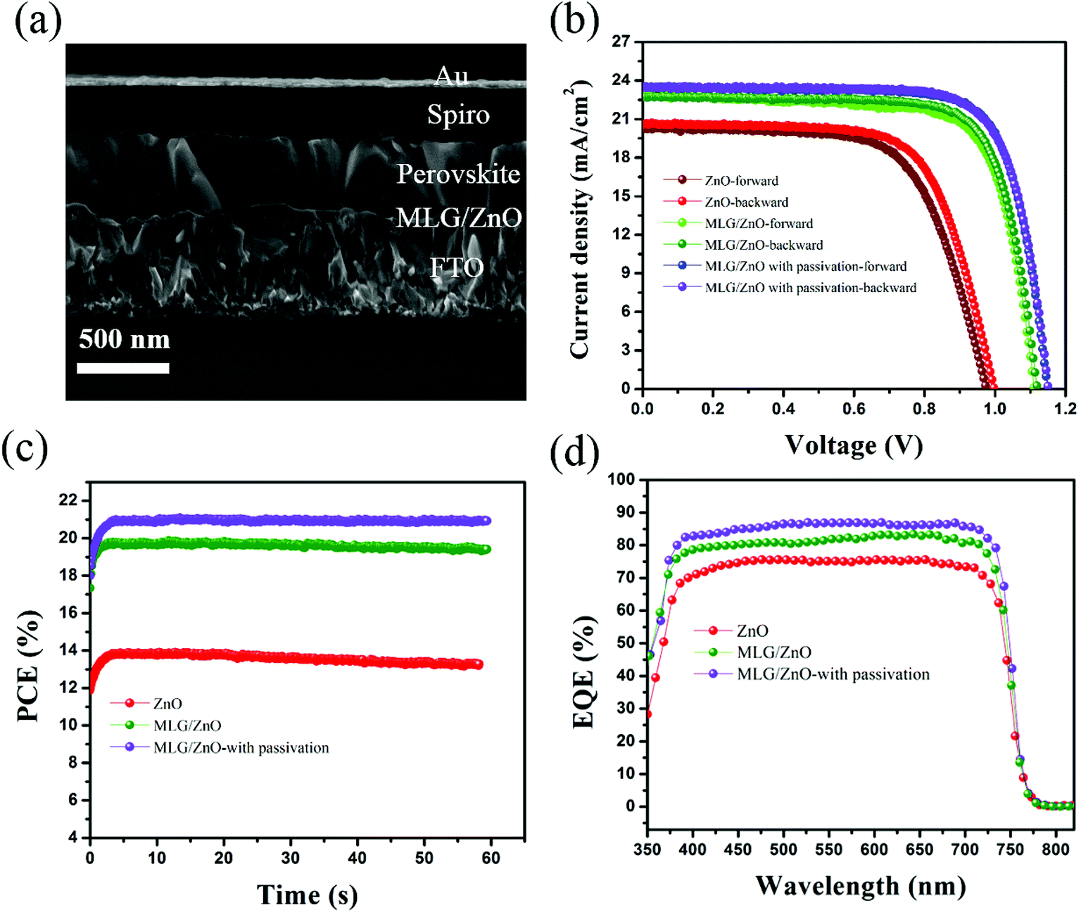 | ||
| Fig. 4 (a) Cross-sectional SEM image of the PSC device based on MLG/ZnO, (b) J–V curves, (c) maximum power point tracking (MPPT) curves, and (d) external quantum efficiency (EQE) spectra of champion PSC devices based on ZnO, MLG/ZnO, and MLG/ZnO-with passivation ETLs. | ||
| Sample | V oc (mV) | J sc (mA cm−2) | FF (%) | PCE (%) | Hysteresis index (%) |
|---|---|---|---|---|---|
| ZnO-forward | 971 | 20.12 | 66.4 | 12.93 | 6.4 |
| ZnO-backward | 996 | 20.63 | 67.3 | 13.82 | |
| MLG/ZnO-forward | 1114 | 22.74 | 77.1 | 19.54 | 1.39 |
| MLG/ZnO-backward | 1120 | 22.71 | 77.9 | 19.81 | |
| MLG/ZnO with passivation-forward | 1149 | 23.39 | 77.5 | 20.82 | 0.91 |
| MLG/ZnO with passivation–backward | 1150 | 23.42 | 78.1 | 21.03 |
To study the role of PFPA passivation in stability, the contact angle of the water droplet was measured on top of the perovskite film deposited on MLG/ZnO without and with passivation. As shown in Fig. 5a and b, this angle is increased from 35° to 62° after surface passivation of the perovskite film with PFPA, indicating less wetting by water for the passivated film. In addition to the contact angle measurement, the stability of devices based on ZnO and MLG/ZnO without and with passivation was tested under continuous illumination (AM 1.5G Sun illumination) at maximum power point tracking at room temperature under a nitrogen environment for 300 hours. As shown in Fig. 5c, the device on the ZnO ETL is not stable over time, due to the reaction between ZnO and perovskite at the interface, accelerated by illumination, as reported in the literature.31 After adding MLG at the interface, the stability of the device is drastically enhanced, where the MLG/ZnO based device without and with passivation retains more than 80% and 93% of its initial PCE value after 300 h, respectively. These results strongly support the role of MLG at the interface in preventing the reaction activated by light over time. We also studied the shelf-life stability of PSC devices kept in an ambient environment (30% relative humidity) over 42 days, as shown in Fig. S8.† Our results show that the stability trends of all devices are more or less the same as those found in the stability test under continuous illumination and in a nitrogen environment. We found that the devices decay slower without applying illumination in ambient air. Moreover, the PCE loss for ZnO-based devices is much lower than that found in the stability test under a nitrogen environment and illumination. This indicates that the reaction between the ZnO ETL and perovskite absorber is accelerated under illumination.
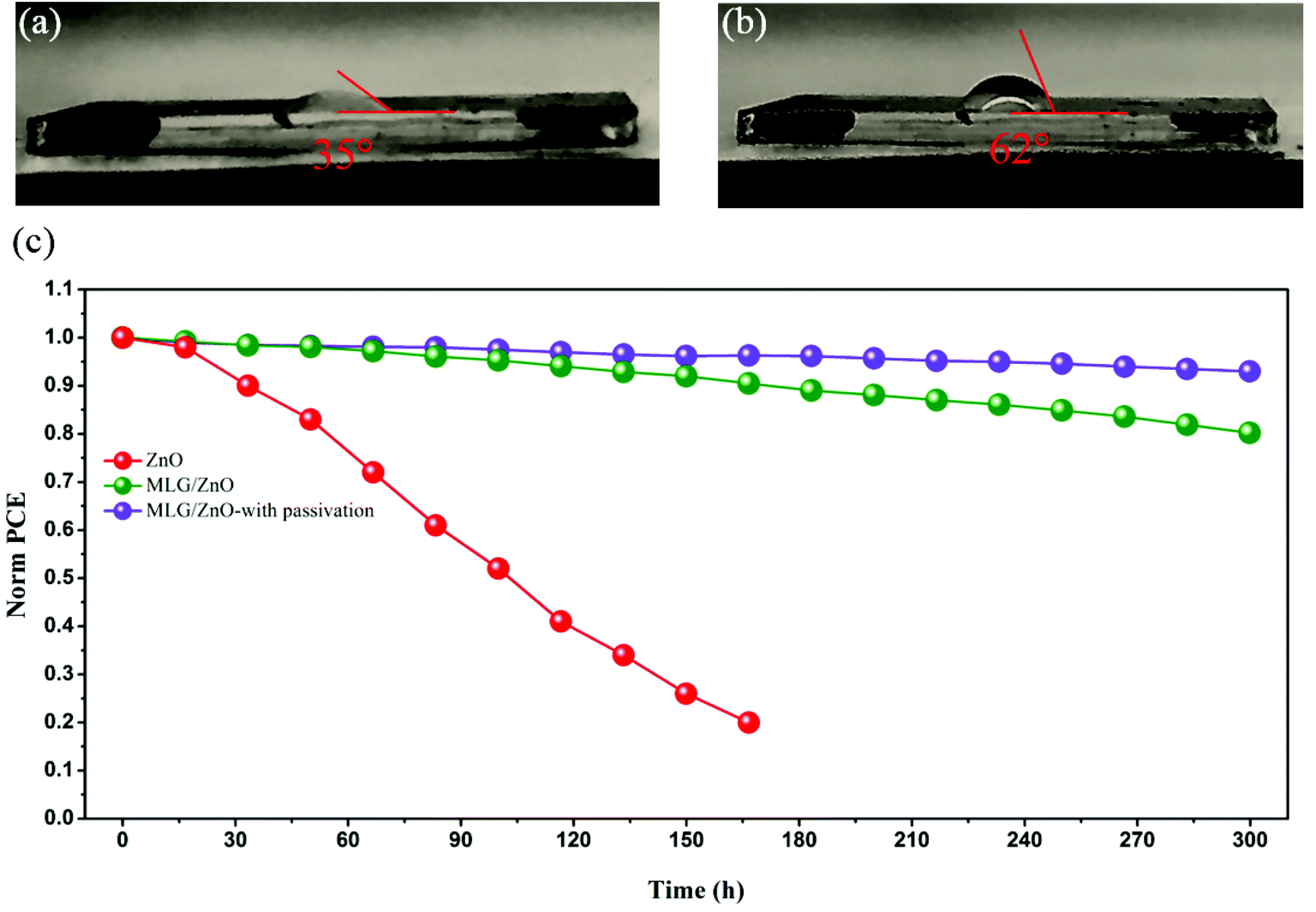 | ||
| Fig. 5 Contact angle measurement of the water droplet on top of the perovskite film deposited on MLG/ZnO without (a) and with (b) PFPA passivation. (c) Stability test of PSC devices based on ZnO, MLG/ZnO, and MLG/ZnO-with passivation under continuous illumination for 300 h at room temperature and under N2 flow. | ||
In order to further study the role of MLG in the PSCs, ultraviolet photoelectron spectroscopy (UPS) was performed for the MLG and ZnO ETL. Fig. S9† shows the UPS measurements and the schematic of the band diagram for the PSC device based on MLG/ZnO. The results show that the Fermi level and the valence band of the ZnO ETL are 4.55 eV and 7.79 eV, respectively. Based on the optical band gap of ZnO (3.35 eV) estimated from the transmittance spectrum (Fig. S9c†), the conduction band of ZnO was calculated to be 4.44 eV. In addition, the work function of MLG was measured (see Fig. S9d†) and the value was 4.38 eV. As seen in the band alignment diagram (Fig. S9e†), MLG could facilitate the extraction of electrons from the perovskite absorber to the ZnO ETL due to its suitable and well-matched work function.
Conclusions
In summary, we applied MLG at the interface of perovskite/ZnO to improve the performance and stability of PSC devices. Our characterization results show that applying MLG not only minimizes the chemical reaction between perovskite and ZnO, but also enhances the carrier extraction properties. In order to further improve the device performance, we have passivated the surface of the perovskite film by using PFPA which mitigates the radiationless charge recombination. Based on ETL modification with MLG and passivation with PFPA, we demonstrate a highly efficient PSC device with a PCE of 21% with negligible hysteresis, which is among the highest values reported for planar PSC devices. More interestingly, our modified device shows excellent operational stability with only 7% PCE loss after 300 h under continuous illumination.Experimental
Synthesis of ZnO nanocrystals
ZnO nanocrystals were prepared as reported elsewhere.24 Briefly, 2.95 g of zinc acetate dihydrate was dissolved in 125 mL methanol at 65 °C with stirring. Another solution containing 1.48 g KOH in 65 mL was prepared and then added into the first solution dropwise at 60–65 °C within 10 min. The mixed solution was stirred for 3 h at the same temperature. After cooling and washing the final product with methanol, the obtained ZnO nanocrystals were dispersed in n-butanol (70 mL), methanol (5 mL) and chloroform (5 mL) to get a solution with a concentration of 6 mg mL−1.Synthesis of mono-layer graphene (MLG)
To synthesize monolayer graphene (MLG), we have used low pressure chemical vapor (LPCVD) deposition using copper foil (Alfa Aesar). First, the copper foil was cleaned by sonication in a nickel etchant (Transene, type TFB) for 2 min, followed by rinsing in deionized (DI) water and drying. Then, MLG was grown on copper foil as can be found in the literature.42Transfer process of MLG
To transfer graphene on top of the ZnO-coated FTO glass, PMMA with 300 nm thickness was spin coated on top of the as-grown graphene/copper. Then, the copper layer was etched using an FeCl3-based copper etchant (Transene). After completely removing the copper, the PMMA/graphene was rinsed in DI water and scooped onto the ZnO-coated FTO glass. After drying, PMMA was removed by immersing in toluene at 60 °C to obtain a PMMA-free, graphene-coated ZnO ETL.Device fabrication
The FTO glasses (NSG-10) were etched and patterned using zinc powder and a solution of 2 M HCl. All FTO glasses were cleaned by immersing them into Triton X-100 (1 vol% in deionized water), DI water, acetone, and ethanol, respectively, followed by 20 min ultrasonication for each step. Then, the substrates were further cleaned by UV ozone treatment. The ZnO ETL was deposited by spin coating of as-synthesized ZnO nanocrystals (3000 rpm for 40 seconds). Before transferring graphene, ZnO-coated FTO glasses were cleaned by UV ozone treatment. Since the graphene surface is hydrophobic, we have employed a two-step deposition method. Perovskite deposition was performed inside a nitrogen filled glovebox. To improve the wettability of the perovskite solution on MLG/ZnO, first, the substrates were treated by spin-coating 50 μL of DMF (6000 rpm for 30 s) before perovskite deposition. Then, a PbI2 solution (600 mg mL−1 DMF) at 100 °C was spin-coated (1500 rpm for 40 s with a ramp rate of 1000 rpm s−1) on top of graphene, followed by annealing at 70 °C for 10 min to obtain a uniform layer of PbI2. In the second step, a mixture of 60 mg formamidinium iodide (FAI), 6 mg of methylammonium bromide (MABr), and 6 mg of methylammonium chloride (MACl) dissolved in 1 mL isopropanol (IPA) was spin-coated on top of the PbI2 layer (3000 rpm for 60 s with a ramp rate of 2000 rpm s−1). Afterwards, the samples were annealed at 150 °C for 30 min in ambient air with a relative humidity of 35%. After cooling the samples, a solution of spiro-OMeTAD (70 mM) in 500 μL chlorobenzene containing 11 μL of bis(trifluoromethylsulfonyl)imide lithium salt (Li-TFSI, Sigma-Aldrich) in acetonitrile (520 mg/1 mL) and 21 μL of (4-tert-butylpyridine-Sigma-Aldrich) was spin-coated at 4000 rpm for 20 s with an accelerating rate of 2000 rpm s−1. Finally, the device was completed by thermal evaporation of gold to obtain an 80 nm thick electrode. The active area of the device was 0.1 cm2.Film characterization
The morphology and grain size of the films were studied by using a ZEISS Merlin high resolution scanning electron microscope (HRSEM) and atomic force microscope (AFM, NanoScope IIIa/Dimension 3100) operating in tapping mode. The crystal structure of monolayer graphene was studied using a high-resolution transmission electron microscope (HRTEM, JOL, JEM-2100, Japan). UV-visible spectra were recorded using a Varian Cary 5. The steady-state photoluminescence (PL) measurements were performed using a Fluorolog 322 (Horiba Jobin Yvon Ltd) setup in a range of 620 nm to 850 nm. The excitation wavelength was fixed at 460 nm. For PL decay measurement, a picosecond pulsed diode laser (EPL-405, excitation wavelength 405 nm, pulse width 49 ps) was used. An Omicron ultrahigh vacuum system using He I (21.2 eV) as the photon source was employed to perform ultraviolet photoelectron spectroscopy (UPS).Device measurement
The photovoltaic parameters were recorded by using a digital source meter (Keithley model 2400, USA). A 450 W xenon lamp (Oriel, USA) was used as the light source. A Schott K113 Tempax sunlight filter (Präzisions Glas & Optik GmbH, Germany) was employed to filter the lamp output. All devices were measured by using a black mask with an active area of 0.16 cm2. The light intensity was 100 mW cm−2 (AM 1.5G). The voltage scan rate was 10 mV s−1. The following formula: hysteresis index = (PCEbackward − PCEforward)/PCEbackward × 100 was used to determine the hysteresis index. Electrochemical impedance spectroscopy (EIS) was performed in a DC bias range (from zero to open circuit voltage (Voc)) with a 10 mV AC perturbation signal. The range of frequency was changed from 1 Hz to 100 kHz. A commercial apparatus (Arkeo-Ariadne, Cicci Research s.r.l.) based on a 300 Watts xenon lamp was used to measure the external quantum efficiency (EQE) spectra.The stability test was performed by using a Biologic MPG2 potentiostat and a white LED lamp to simulate standard AM 1.5G conditions with an active area of 0.1 cm2. Here, the maximum power point (MPP) was tracked under continuous full sun illumination and nitrogen flow and updated every 10 s. The substrate temperature was controlled using a Peltier element during the test, which was in direct contact with the back of the device. In addition, the J–V curve of the device was measured every 10 min to track all photovoltaic parameters.
Electron beam induced current (EBIC) images were taken using a FEI Helios scanning electron microscope (SEM). The voltage and current of the electron beam were 10 kV and 170 pA, respectively. The beam was applied on top of a gold electrode in order to excite a constant number of carriers.
Conflicts of interest
There is no conflict to declare.Acknowledgements
This work was sponsored by ENI S.p.A under the MITEI Solar Frontier Center. M. M. T wants to thank the laboratory of photonics and interfaces (LPI) at Ecole Polytechnique Fédérale de Lausanne (EPFL).Notes and references
- M. M. Tavakoli, W. Tress, J. V. Milić, D. Kubicki, L. Emsley and M. Grätzel, Energy Environ. Sci., 2018, 11, 3310–3320 RSC.
- D. Prochowicz, P. Yadav, M. Saliba, D. J. Kubicki, M. M. Tavakoli, S. M. Zakeeruddin, J. Lewiński, L. Emsley and M. Grätzel, Nano Energy, 2018, 49, 523–528 CrossRef CAS.
- W. S. Yang, B. W. Park, E. H. Jung, N. J. Jeon, Y. C. Kim, D. U. Lee, S. S. Shin, J. Seo, E. K. Kim, J. H. Noh and S. I. Seok, Science, 2017, 356, 1376–1379 CrossRef CAS PubMed.
- M. M. Tavakoli, S. M. Zakeeruddin, M. Grätzel and Z. Fan, Adv. Mater., 2018, 30, 1705998 CrossRef PubMed.
- Q. Lin, L. Lu, M. M. Tavakoli, C. Zhang, G. C. Lui, Z. Chen, X. Chen, L. Tang, D. Zhang, Y. Lin and P. Chang, Nano Energy, 2016, 22, 539–547 CrossRef CAS.
- National Center for Photovoltaics (NCPV) at the National Renewable Energy Laboratory (NREL); https://www.nrel.gov/pv/assets/images/efficiency-chart.png.
- S. F. Leung, Q. Zhang, M. M. Tavakoli, J. He, X. Mo and Z. Fan, Small, 2016, 12, 2536–2548 CrossRef CAS PubMed.
- C. Zuo, H. J. Bolink, H. Han, J. Huang, D. Cahen and L. Ding, Adv. Sci., 2016, 3, 1500324 CrossRef PubMed.
- M. M. Tavakoli, K. H. Tsui, Q. Zhang, J. He, Y. Yao, D. Li and Z. Fan, ACS Nano, 2015, 9, 10287–10295 CrossRef CAS PubMed.
- W. Chen, Y. Wu, Y. Yue, J. Liu, W. Zhang, X. Yang, H. Chen, E. Bi, I. Ashraful, M. Grätzel and L. Han, Science, 2015, 350, 944–948 CrossRef CAS PubMed.
- M. M. Tavakoli, L. Gu, Y. Gao, C. Reckmeier, J. He, A. L. Rogach, Y. Yao and Z. Fan, Sci. Rep., 2015, 5, 14083 CrossRef PubMed.
- J. Min, Z. G. Zhang, Y. Hou, C. O. Ramirez Quiroz, T. Przybilla, C. Bronnbauer, F. Guo, K. Forberich, H. Azimi, T. Ameri, E. Spiecker, Y. Li and C. J. Brabec, Chem. Mater., 2015, 27, 227–234 CrossRef CAS.
- M. M. Tavakoli, F. Giordano, S. M. Zakeeruddin and M. Grätzel, Nano Lett., 2018, 18, 2428–2434 CrossRef CAS PubMed.
- S. Song, G. Kang, L. Pyeon, C. Lim, G. Y. Lee, T. Park and J. Choi, ACS Energy Lett., 2017, 2, 2667–2673 CrossRef CAS.
- C. Wehrenfennig, M. Liu, H. J. Snaith, M. B. Johnston and L. M. Herz, Energy Environ. Sci., 2014, 7, 2269–2275 RSC.
- Q. Jiang, L. Zhang, H. Wang, X. Yang, J. Meng, H. Liu, Z. Yin, J. Wu, X. Zhang and J. You, Nat. Energy, 2017, 2, 16177 CrossRef CAS.
- M. M. Tavakoli, A. Simchi, X. Mo and Z. Fan, Mater. Chem. Front., 2017, 1, 1520–1525 RSC.
- H. Tan, A. Jain, O. Voznyy, X. Lan, F. P. G. de Arquer, J. Z. Fan, R. Quintero-Bermudez, M. Yuan, B. Zhang, Y. Zhao and F. Fan, Science, 2017, 355, 722–726 CrossRef CAS PubMed.
- M. M. Tavakoli, A. Simchi, Z. Fan and H. Aashuri, Chem. Commun., 2016, 52, 323–326 RSC.
- M. M. Tavakoli, R. Tavakoli, S. Hasanzadeh and M. H. Mirfasih, J. Phys. Chem. C, 2016, 120, 19531–19536 CrossRef CAS.
- S. F. Leung, Q. Zhang, M. M. Tavakoli, J. He, X. Mo and Z. Fan, Small, 2016, 12, 2536–2548 CrossRef CAS PubMed.
- M. Shirazi, R. S. Dariani and M. R. Toroghinejad, J. Alloys Compd., 2017, 692, 492–502 CrossRef CAS.
- R. Azmi, W. T. Hadmojo, S. Sinaga, C. L. Lee, S. C. Yoon, I. H. Jung and S. Y. Jang, Adv. Energy Mater., 2018, 8, 1870022 CrossRef.
- M. M. Tavakoli, R. Tavakoli, Z. Nourbakhsh, A. Waleed, U. S. Virk and Z. Fan, Adv. Mater. Interfaces, 2016, 3, 1500790 CrossRef.
- F. Yang, D. W. Kang and Y. S. Kim, RSC Adv., 2017, 7, 19030–19038 RSC.
- X. Dong, H. Hu, B. Lin, J. Ding and N. Yuan, Chem. Commun., 2014, 50, 14405–14408 RSC.
- X. Zhao, H. Shen, Y. Zhang, X. Li, X. Zhao, M. Tai, J. Li, J. Li, X. Li and H. Lin, ACS Appl. Mater. Interfaces, 2016, 8, 7826–7833 CrossRef CAS PubMed.
- M. M. Tavakkoli and S. M. Abbasi, Mater. Des., 2013, 46, 573–578 CrossRef CAS.
- Y. Cheng, Q. D. Yang, J. Xiao, Q. Xue, H. W. Li, Z. Guan, H. L. Yip and S. W. Tsang, ACS Appl. Mater. Interfaces, 2015, 7, 19986–19993 CrossRef PubMed.
- M. M. Tavakoli, R. Tavakoli, P. Davami and H. Aashuri, J. Comput. Electron., 2014, 13, 425–431 CrossRef CAS.
- W. Zhang, J. Xiong, L. Jiang, J. Wang, T. Mei, X. Wang, H. Gu, W. A. Daoud and J. Li, ACS Appl. Mater. Interfaces, 2017, 9, 38467–38476 CrossRef CAS PubMed.
- J. Cao, B. Wu, R. Chen, Y. Wu, Y. Hui, B. W. Mao and N. Zheng, Adv. Mater., 2018, 30, 1705596 CrossRef PubMed.
- M. M. Tavakoli, M. Saliba, P. Yadav, P. Holzhey, A. Hagfeldt, S. M. Zakeeruddin and M. Graetzel, Adv. Energy Mater., 2018, 1802646 CrossRef.
- M. Yavari, M. Mazloum-Ardakani, S. Gholipour, M. M. Tavakoli, S. H. Turren-Cruz, N. Taghavinia, M. Grätzel, A. Hagfeldt and M. Saliba, Adv. Energy Mater., 2018, 8, 1800177 CrossRef.
- M. M. Tavakoli, A. Waleed, L. Gu, D. Zhang, R. Tavakoli, B. Lei, W. Su, F. Fang and Z. Fan, Nanoscale, 2017, 9, 5828–5834 RSC.
- X. Zheng, B. Chen, J. Dai, Y. Fang, Y. Bai, Y. Lin, H. Wei, X. C. Zeng and J. Huang, Nat. Energy, 2018, 2, 17102 CrossRef.
- M. M. Tavakoli, P. Yadav, R. Tavakoli and J. Kong, Adv. Energy Mater., 2018, 8, 1800794 CrossRef.
- T. Li, Y. Pan, Z. Wang, Y. Xia, Y. Chen and W. Huang, J. Mater. Chem. A, 2017, 5, 12602–12652 RSC.
- M. M. Tavakoli, A. Simchi and H. Aashuri, Mater. Chem. Phys., 2015, 156, 163–169 CrossRef CAS.
- N. K. Noel, A. Abate, S. D. Stranks, E. S. Parrott, V. M. Burlakov, A. Goriely and H. J. Snaith, ACS Nano, 2014, 8, 9815–9821 CrossRef CAS PubMed.
- M. M. Tavakoli, D. Bi, L. Pan, A. Hagfeldt, S. M. Zakeeruddin and M. Grätzel, Adv. Energy Mater., 2018, 8, 1800275 CrossRef.
- Y. Song, S. Chang, S. Gradecak and J. Kong, Adv. Energy Mater., 2016, 6, 1600847 CrossRef.
Footnote |
| † Electronic supplementary information (ESI) available. See DOI: 10.1039/c8ta10857a |
| This journal is © The Royal Society of Chemistry 2019 |