
 Open Access Article
 This Open Access Article is licensed under a
 Creative Commons Attribution 3.0 Unported Licence
Realizing high thermoelectric performance in Cu2Te alloyed Cu1.15In2.29Te4†
Min
Li
ab,
Yong
Luo
*a,
Gemei
Cai
 c,
Xie
Li
b,
Xiaoyan
Li
d,
Zhongkang
Han
*d,
Xinyi
Lin
e,
Debalaya
Sarker
*f and
Jiaolin
Cui
*b
c,
Xie
Li
b,
Xiaoyan
Li
d,
Zhongkang
Han
*d,
Xinyi
Lin
e,
Debalaya
Sarker
*f and
Jiaolin
Cui
*b
aSchool of Materials Science and Engineering, China University of Mining and Technology, Xuzhou 221116, China. E-mail: sulyflying@cumt.edu.cn
bSchool of Materials & Chemical Engineering, Ningbo University of Technology, Ningbo 315016, China. E-mail: cuijiaolin@163.com
cSchool of Materials Science and Engineering, Central South University, Changsha 410083, China
dDivision of Interfacial Water and Key Laboratory of Interfacial Physics and Technology, Shanghai Institute of Applied Physics, Chinese Academy of Sciences, Shanghai, 201800, China. E-mail: hegongdahuagong@126.com
eDepartment of Mechanical Engineering and Materials Science, Duke University, Durham, North Carolina 27708, USA
fTheory Department, Fritz Haber Institute of the Max-Planck-Society, Faradayweg 4-6, D-14195 Berlin, Germany. E-mail: sarker@fhi-berlin.mpg.de
First published on 24th December 2018
Abstract
Controlling the chemical and physical structure at the atomic level is of paramount importance for decreasing the thermal conductivity by enhancing phonon scattering in thermoelectric materials. Additional enhancement in the figure of merit (ZT) can be achieved by improving the electron transport properties. Cu-deficient ternary I–III–VI compounds have received increasing attention because they can easily form solid solutions and thereby their thermoelectric performance can be readily engineered. In this work, we present a novel thermoelectric compound Cu1.15In2.29Te4 with the dimensionless figure of merit ZT ∼ 1.0 through alloying with Cu2Te. The enhanced ZT value is mainly attributed to the ultralow lattice thermal conductivity (κL = 0.24 W K−1 m−1 at 825 K), caused by a pronounced local lattice disorder as a result of the interstitial residing of extra Te. Density functional theory based first-principles calculations further elucidate that the creation of the resonant states at the Fermi level and impurity levels near the valence band edge has increased the effective mass and carrier concentration, resulting in the improved electrical properties. Moreover, the localized modes of the Te interstitial defects hybridize with the acoustic modes of stoichiometric In and Te and lead to the enhanced scattering of the thermal phonons resulting in the significantly low κL. The above findings substantiate that appropriate doping of Cu2Te in the newly developed Cu1.15In2.29Te4 compound can effectively manipulate both electron and phonon transport and thereby promises high thermoelectric performance.
1. Introduction
Thermoelectric (TE) materials have attracted significant attention lately because of their potential as source materials for power generation.1–5 The limitation for large-scale applications of thermoelectrics is their low conversion efficiency, which is mainly governed by the dimensionless figure of merit (ZT), ZT = Tα2σ/κ, where T, α, σ, and κ are, respectively, the absolute temperature, Seebeck coefficient, electrical conductivity, and total thermal conductivity consisting of lattice (κL) and electronic (κe) parts mainly. In order to enhance the ZT value, it is essential to improve the power factor PF, PF = α2σ, and at the same time reduce the thermal conductivity κ. Since all these three parameters α, σ, and κe are dependent on the carrier concentration, it is therefore difficult to enhance the ZT value by simply manipulating one of these parameters.The practical strategies for improving the ZT of existing materials are typified either by enhancing the power factor α2σ via band structure engineering,3–6 or by reducing the lattice thermal conductivity (κL) via various approaches, such as nanostructure engineering,7,8 development of liquid-like Cu2−xSe9,10 and intrinsically strong lattice anharmonicity of TE materials.11–14 Apart from the aforementioned approaches, an alternate, for instance, can be the creation of point defects on an atomic scale, like interstitial,15–17 substitutional18,19 or vacancy20–23 in bulk TE materials. This indeed improves the TE performance by lowering the lattice part (κL < 0.4 W K−1 m−1) of the thermal conductivity at high temperatures.24–26
Owing to the inherent unique crystal structure and/or the presence of cation vacancies, Cu–In–Te ternary compounds with a chalcopyrite structure (s.g. I![[4 with combining macron]](https://www.rsc.org/images/entities/char_0034_0304.gif) 2d) have recently attracted much attention in thermoelectrics.27–31 Examples include CuInTe2-based compounds with ZT values of 1.52–1.72 at 823–850 K,27,28 achieved by introduction of In2O3 (ref. 27) and ZnS,28 as the grain or phase boundaries introduced by impurity act as a nanoscale heterostructure barrier blocking both holes and phonons.
2d) have recently attracted much attention in thermoelectrics.27–31 Examples include CuInTe2-based compounds with ZT values of 1.52–1.72 at 823–850 K,27,28 achieved by introduction of In2O3 (ref. 27) and ZnS,28 as the grain or phase boundaries introduced by impurity act as a nanoscale heterostructure barrier blocking both holes and phonons.
From the structural point of view, the compound Cu1.15In2.29Te4 can be a potential TE candidate in a sense that there is at least one kind of intrinsic point defect in its crystal structure, that is, ∼14% copper vacancies. These vacancies, similar to those observed in Cu4−δGa4Te8 (δ = 1.12)23 and Cu18Ga25Te50 (ref. 32), are of great significance for engineering the point defects, as the vacancy concentration can be easily controlled through the incorporation of impurities.21,33–35 On the other hand, the incorporation of impurities into vacancies would often unpin the Fermi level or create impurity bands within the gap, which yields a local lattice distortion and alters the basic conducting mechanism as well.
In this work, we present a potential ternary TE compound Cu1.15In2.29Te4 with a highest ZT value of 0.53 at 822 K. Through alloying Cu2Te to form solid solutions (Cu2Te)δ(Cu1.15In2.29Te4) (δ = 0.025–0.075), an interstitial occupation of element Te is observed. The interstitial Te in-turn forms impurity bands within the energy gap and thus enhances the Hall carrier concentration. Along with the ultralow lattice thermal conductivity due to the introduction of point defects, the highest ZT value of ∼1.0 for δ = 0.05 has been achieved at 825 K.
2. Experimental
2.1 Sample preparation
The mixtures, according to the formula (Cu2Te)δ(Cu1.15In2.29Te4) (δ = 0, 0.025, 0.0375, 0.05, 0.075), have been loaded into five different vacuum silica tubes and are heated to 1123 K with a heating rate of ∼5° min−1, followed by holding at this temperature for 24 h and then rapid cooling in water. After that, the ingots are annealed at 900 K for 72 h, and then are cooled down to RT in a furnace.After ball milling of the ingots at a rotation rate of 350 rpm for 5 h, the dried powders are quickly sintered using spark plasma sintering apparatus (SPS-1030) using a programmed sintering procedure. The highest sintering temperature is fixed to be ∼900 K at which the sintered bulks are kept for 2 min. The sintering pressure is maintained at 60 MPa. Subsequently, the sintered bulks are cooled to RT in a furnace. The final samples for electrical property measurements are 3 mm in thickness and 2.5 mm × 12 mm in cross-section. These numbers are obtained from the sintered blocks with a size of ϕ 10 mm × 2.5 mm. After polishing the surfaces of two sides, the coin-shaped sintered blocks with the size of ϕ 10 mm × 1.5 mm are prepared for thermal diffusivity measurements. Although the thermal diffusivities (λ) and electrical properties (α and σ) are measured along different pressing directions, previous studies23,32,36 reveal that there is only marginal error (usually less than 5%) introduced in TE performances in the case of isotropic samples as compared to measurements along the same direction. It should be mentioned that all sintered bulks have a density (d) above 93.0–94.0% of the theoretical density (6.087 × 10⁻³ kg cm−3) of CuInTe2.
2.2 Physical property measurements
Hall coefficients (RH) are measured with a four-probe configuration in the system (PPMS, Model-9) with a magnetic field of up to ±2 T. The Hall mobility (μ) and carrier concentration (nH) are calculated according to the relations μ = |RH|σ and nH = 1/(eRH), respectively, where e is the electron charge. The Seebeck coefficients (α) and electrical conductivities (σ) are measured by using a ULVAC ZEM-3 instrument system under a helium atmosphere from RT to ∼830 K, with a measurement uncertainty of ∼6.0% for both the Seebeck coefficient and electrical conductivity.The thermal conductivities are then calculated based on the equation κ = dλCp, where the thermal diffusivity λ is measured with the laser flash method (TC-1200RH) under vacuum. The heat capacities (Cp) are estimated based on the Dulong–Petit rule above RT. The three physical parameters (α, σ, and κ) are finalized by taking the average values of several samples tested by the same method. The total uncertainty of the ZT value is about 18%. The lattice contributions (κL) are obtained by subtracting the electronic contribution (κe) from the total κ, i.e., κL = κ − κe. Here κe is expressed by the Wiedemann–Franz relation, κe = L0σT, where L0 is the Lorenz number, estimated using the expression L0 = 1.5 + exp(−|α|/116)37 (where L0 is in 10−8 W Ω K−2 and |α| in μV K−1).
2.3 Characterization
The chemical compositions of the samples (δ = 0, 0.05) are checked using an electron probe micro-analyzer (EPMA) (S-4800, Hitachi, Japan) with an accuracy > 97%. The microstructures of the samples (δ = 0, 0.05) have been examined using high-resolution transmission electron microscopy (HRTEM). HRTEM images are obtained at 220 kV using a JEM-2010F (Field emission TEM).The XRD patterns are collected using a powder X-ray diffractometer (D8 Advance) operating at 50 kV and 40 mA under Cu Kα radiation (λ = 0.15406 nm) and at a scan rate of 4° min−1 in the range from 10° to 110°. Besides, X'Pert Pro, PANalytical code is used to perform the Rietveld refinement of the XRD patterns of the pristine Cu1.15In2.29Te4 and Cu2Te-alloyed samples. The lattice constants are then obtained from the refinement of the X-ray patterns using Jade software.
3. Methodology: theory
Density functional theory based first-principles calculations are carried out using FHI-aims code,38,39 which is an all electron, full potential electronic structure code that uses a numeric, atom-centered basis set. The electronic exchange and correlation is treated with the generalized gradient approximation (GGA) of Perdew–Burke–Ernzerhof (PBE).40 All the numeric settings are so chosen that an energy convergence less than 10−3 eV is achieved. Both the atomic positions and the lattice vectors are allowed to fully relax using Broyden–Fletcher–Goldfarb–Shanno (BFGS) algorithm using a 4 × 4 × 2 k-grid. Further the electronic structure is analyzed and verified with the hybrid functional HSE06,41 which takes into account part of the exact exchange with a denser k-grid 6 × 6 × 3. The phonon dispersions are calculated using the finite displacement method, as implemented in PHONOPY code.424. Results and discussion
4.1 Compositions and structures
Scanning electron microscopy (S-4800, Hitachi, Japan) is employed to check the microstructures and homogeneity of the sample. Fig. S1a and b† show SEM images of the freshly fractured surfaces of (Cu2Te)δ(Cu1.15In2.29Te4) (δ = 0.05). The EDAX spectrum and mapping pictures for the three elements Cu, In, Te are shown in Fig. S1c–f.† The EDAX spectrum and mapping pictures of other samples are not shown here. It is observed that there are slight segregations of the three elements inside the matrix, indicating that the three elements are not distributed perfectly. A further detection reveals that the segregation should occur in different grains rather than in different phases, as the materials exhibit a single phase (see the discussion below). The average chemical compositions obtained from several mappings are presented in Table S1,† where the numbers of moles of Te are normalized to 4.0 (for δ = 0) and 4.05 (for δ = 0.05) (the actual moles of Te are slightly less than nominal ones). In this case, the normalized moles of Cu and In are a little higher than nominal ones. This suggests that there is a subtle deficiency in Te, which is mainly ascribed to the evaporation of Te during the preparation of the materials.Rietveld refinements using the XRD data of Cu2Te-alloyed samples are next conducted, as shown in Fig. S2.† The experimental parameters of powder X-ray diffraction and refined crystallographic data of (Cu2Te)δ(Cu1.15In2.29Te4) (δ = 0, 0.0375, 0.05 and 0.075) are shown in Table S2.†
Based on the refinement data, it is found that all peak positions are the same as those of CuInTe2 (PDF: 65-0245; s.g.: I2d(122)), indicating that the materials crystallize in a Cu-deficient CuInTe2 phase without visible impurities being precipitated. Besides, the lattice constants (a) tend to increase as the Cu2Te content increases (Fig. 1a and Table S2†). As such, it is determined that Cu2Te is incorporated into the lattice structure, which causes a dilation of the lattice structure and local lattice distortion.
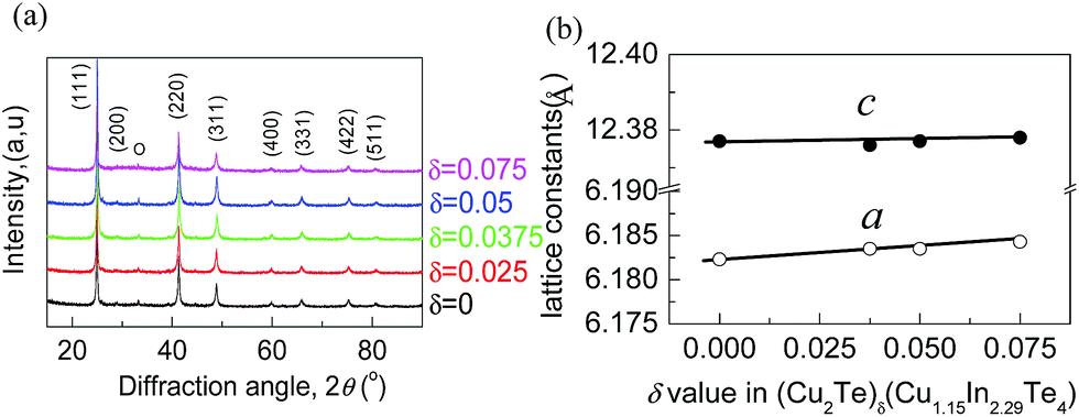 | ||
| Fig. 1 (a) XRD patterns of the powders of (Cu2Te)δ(Cu1.15In2.29Te4) (δ = 0–0.075). All peak positions can be indexed to the compound CuInTe2 (PDF: 65-0245). (b) Relationship between the lattice constants and Cu2Te content. It is observed that the lattice parameter a increases almost linearly, and follows Vegard's law. | ||
In order to further confirm the synthesis of Cu1.15In2.29Te4-based alloys, the microstructures of the samples at δ = 0 and 0.05 have been examined by using high-resolution TEM (HRTEM). Fig. S3a† shows the TEM image of the sample at δ = 0, and Fig. S3b† shows its corresponding selected area electron diffraction (SAED); Fig. S3c† shows the corresponding HRTEM image. The inset in Fig. S3c† shows a magnified image of the same, which shows that the d spacing between (111) crystal planes is about 0.352 nm. Fig. S3d† shows the EDS measurement result, which shows that the material consists of three elements, Cu, In and Te, only.
Fig. S4a and b† show the TEM and the corresponding HRTEM images for the sample at δ = 0.05. Fig. S4c† shows the SAED pattern and Fig. S4d† a magnified high-resolution TEM image, which shows that the d spacing between (111) crystal planes is 0.355 nm. The slight increase in d spacing upon an addition of Cu2Te might have resulted from the dilation of the crystal lattice, and is in accordance with the increased lattice constants from XRD analyses. The above observations further confirm the synthesizing of the (Cu2Te)δ(Cu1.15In2.29Te4) alloys.
4.2 The local & electronic structure from first-principles calculations
To understand the local atomic structural arrangements in the doped Cu1.15In2.29Te4 and pristine samples, and their effect on the thermoelectric properties of materials, we have calculated the electronic structures of the compounds with different arrangements of atoms. The large systems of Cu20In40Te72 and Cu22In40Te73 were used to simulate the structures of Cu1.15In2.29Te4 and Cu2Te doped Cu1.15In2.29Te4, respectively. Note that, to obtain the most stable structure of Cu22In40Te73 with extra Cu2Te, we have systematically calculated all the possible sites for the extra Te atom, including the interstitial site with a neighbor Cu vacancy, the Cu vacancy site, the interstitial site without a neighboring Cu vacancy, and the In vacancy site and the corresponding In atom located at a Cu vacancy site. It is found that the structure having an interstitial Te atom with a neighboring Cu vacancy is the most stable structure (see Fig. S5†). According to Boltzmann distribution at our experimental temperature range, the interstitially occupied Te is the main species for the extra Te, which might be the origin of the crystal structure expansion observed in Fig. 1b. The most stable structures of Cu20In40Te72 and Cu22In40Te73, obtained after sampling different configurational isomers mentioned above, are shown in Fig. 2.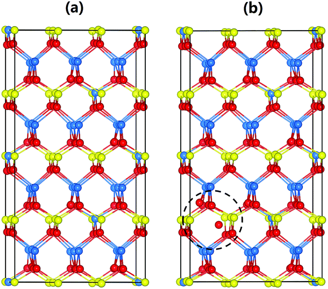 | ||
| Fig. 2 Atomic arrangements of (a) Cu20In40Te72 and (b) Cu22In40Te73. Cu, In, and Te atoms are shown in yellow, blue, and red, respectively. The interstitial Te and its local disorders are highlighted with a dashed circle. | ||
The electronic density of states (DOS) of Cu20In40Te72 and Cu22In40Te73 is plotted in Fig. 3a and b, respectively. Fig. 3c and d show the magnified images of them near the Fermi level (EFermi), respectively. It is observed that near VBM states of stoichiometric Te and In are already present in the pristine material (Fig. 3c), and after doping the hybridized states get more enhanced and shifted towards the Fermi level (Fig. 3d). This clear enhancement in the near-Fermi level states explains the formation of an impurity band (IB) near the valence band maxima (VBMs), which is a result of the hybridization of interstitial Te with stoichiometric In and Te states. Besides, the band structure of the doped alloy reveals the formation of an IB near the valence band maximum (VBM), as shown in Fig. S6† (red line). The IB is critical for the transport of carriers, and it serves as the conducting pathway for holes in the p-type semiconductors, firstly from the VB to the IB, and subsequently to the CB (VB → IB → CB).43,44
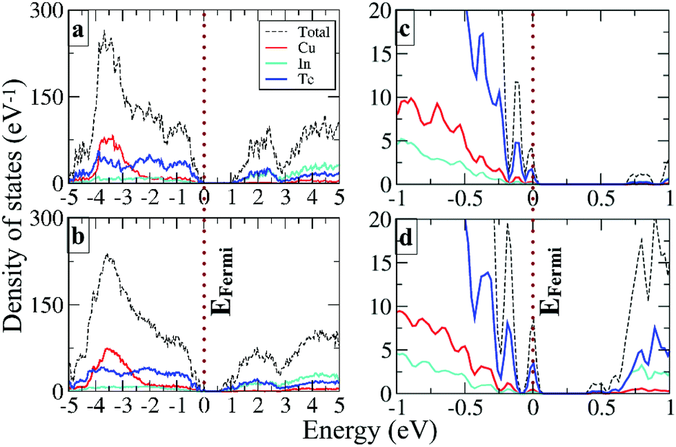 | ||
| Fig. 3 The electronic density of states calculated at the HSE06 level of theory for (a) Cu20In40Te72 and (b) Cu22In40Te73. (c) and (d) The zoomed views of the same near the Fermi level (EFermi), respectively. | ||
4.3 Transport properties
Since the electronic structure gets modified due to the increased Cu and Te content, it is believed that the charge transport properties in the system would get modified accordingly. In order to verify this speculation, we have measured the Hall coefficients of (Cu2Te)δ(Cu1.15In2.29Te4) (δ = 0, 0.025, 0.0375, 0.050, 0.075) near RT and then calculated the Hall carrier concentration (nH) and mobility (μ). The results are shown in Fig. 4, where we can see that the nH value increases from 1.96 × 1018 cm−3 (at δ = 0) to 6.73 × 1018 cm−3 (at δ = 0.05) as the Cu2Te content increases, followed by a decrease at δ > 0.05, while the mobility μ decreases from 25.0 cm2 V−1 s−1 (at δ = 0) to 10.59 cm2 V−1 s−1 (at δ = 0.05), followed by an increase to 21.17 cm2 V−1 s−1 (at δ = 0.075). The enhancement in nH at δ ≤ 0.05 is attributed to the creation of the impurity band (IB) within the gap, since the impurity band, as mentioned above, acts like a catalyst that promotes the transport of carriers, thus increasing the number of mobile charge carriers available for electrical conduction, as those observed in Tl-PbTe or Sn-β-As2Te3 systems.45,46 However, the impurity band has another effect: acting as an electron and hole (e–h) recombination center.47 Therefore, the reduction in nH and increase in μ at δ > 0.05 might be due to the e–h recombination.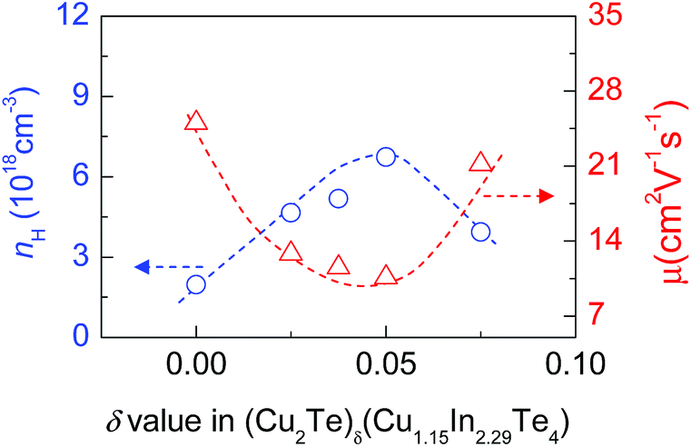 | ||
| Fig. 4 Measured Hall carrier concentration (nH) and mobility (μ) of (Cu2Te)δ(Cu1.15In2.29Te4) (δ = 0–0.075) near RT as a function of Cu2Te content (δ value). | ||
4.4 TE performance
We see in Fig. 5 that the Seebeck coefficient (α) (for both pristine and doped systems) increases first with increasing temperature up to ∼600 K. After reaching the maximum value, it starts decreasing again for all the systems. Note that, all the α values are positive. In addition, the highest α value tends to decrease from 318.0 to 296.0 μV K−1 as the Cu2Te content (δ value) increases, as shown in Fig. 5a. Since the Seebeck coefficient is closely related to two parameters i.e., carrier concentration and effective mass, we will next analyze their roles separately.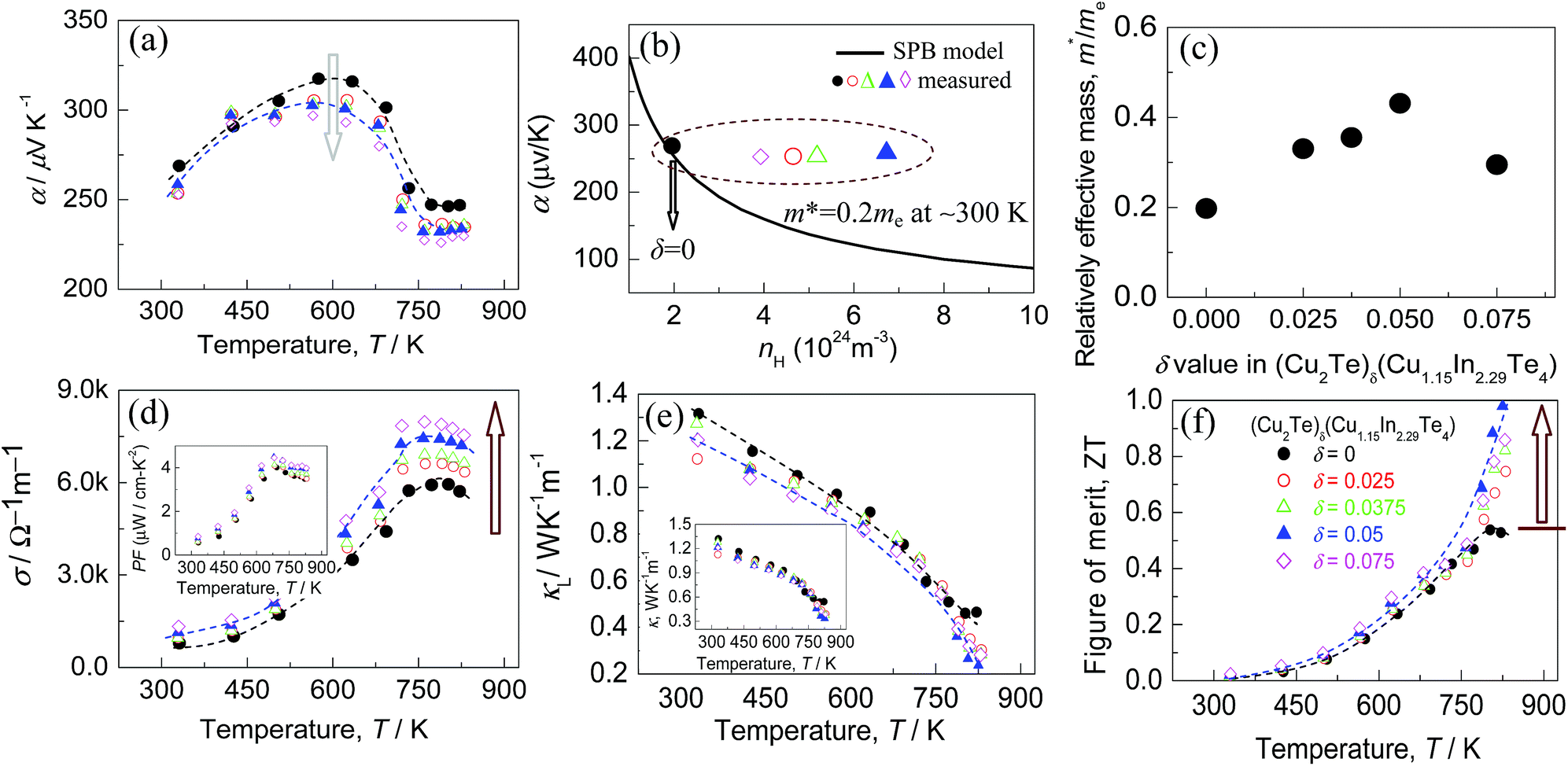 | ||
Fig. 5 TE properties as a function of temperature for the compounds (Cu2Te)δ(Cu1.15In2.29Te4) (δ = 0–0.075). (a) Seebeck coefficients as a function of temperature; (b) experimentally determined Seebeck coefficients (α) at the corresponding Hall carrier concentrations, labeled by  . The solid line represents the Pisarenko relation at RT, assuming that the effective mass m* is 0.2me; (c) effective mass m* as a function of Cu2Te content; (d) electrical conductivities (σ) of different materials (δ values), the inset shows the power factor PF, PF = α2σ; (e) lattice thermal conductivities κL of the different materials (δ values), the inset shows the total thermal conductivities κ; (f) ZT value as a function of temperature of different materials (δ values). . The solid line represents the Pisarenko relation at RT, assuming that the effective mass m* is 0.2me; (c) effective mass m* as a function of Cu2Te content; (d) electrical conductivities (σ) of different materials (δ values), the inset shows the power factor PF, PF = α2σ; (e) lattice thermal conductivities κL of the different materials (δ values), the inset shows the total thermal conductivities κ; (f) ZT value as a function of temperature of different materials (δ values). | ||
To understand the change in the effective mass (m*), we plot the dependence of the Seebeck coefficients on the Hall carrier concentration in Fig. 5b, assuming that the Pisarenko relation48 with the SPB model is valid in Cu–In–Te systems.49,50 This dependence indicates that α values of samples alloyed with Cu2Te (by a dotted circle) are higher than those predicted by the Pisarenko relation at the corresponding carrier concentrations. The solid line depicted in Fig. 5b corresponds to the relationship between α and nH for Cu1.15In2.29Te4 (δ = 0) at RT with an effective mass of m* = 0.20 me. This result obviously suggests that the effective mass increases after alloying with Cu2Te. In fact, the effective masses (m*) are calculated using the Pisarenko relation, as shown in Fig. 5c, where the m* value increases from m* = 0.20 me (δ = 0) to 0.44 me (δ = 0.05), lower than the 1.18 ± 0.35 me in Cu3In7Te12.51 The enhancement in m* should result from the creation of the resonant state at EFermi. Since the Seebeck coefficient is proportional to the m* according to the Pisarenko relation, it is therefore believed that the decrease of α value when the δ value increases is mainly attributed to the fact that the effect of the carrier concentration neutralizes that of effective mass. Also, the Seebeck coefficients at δ = 0.075 are lower than those of other counterparts, which might be a joint result of nH (Fig. 4) and m* values (Fig. 5c).
The electrical conductivities (σ) against temperature is plotted in Fig. 5d, where the inset shows the power factor PF (PF = α2σ) of different materials (δ values). Generally, σ increases with increasing Cu2Te content, and so does the power factor PF. At δ = 0.075, the σ value reaches the highest 7.8 × 10³ Ω−1 m−1 at ∼750 K, even though the nH value reduces at δ = 0.075. Therefore, the origin for the improved electrical conductivity (σ) at a higher δ value is a combined effort of the carrier concentration and mobility (μ). Furthermore, the PF reaches the highest 4.45 μW cm−1 K−2 at 681 K, which is higher than that of CuInTe2 (1.77 μW cm−1 K−2)52 but lower than those of Cu-deficient CuInTe2 (9.23–13.7 μW cm−1 K−2).33,50,51,53,54
Fig. 5e shows the lattice thermal conductivities (κL) of different materials as a function of temperature. Generally, the κL values decrease with rising temperature. When the temperature increases to the highest (∼825 K), the lattice part of the thermal conductivity for δ = 0.05 drops to the minimum (0.24 W K−1 m−1). This value is lower than those (∼0.47 W K−1 m−1) at δ = 0 and (∼0.28 W K−1 m−1) at δ = 0.075. Apart from that, the κL value tends to decrease as the δ value increases. Furthermore, the resemblance between the lattice parts and those of total κ (the inset in Fig. 5e) suggests that the phonon transport plays a major role in heat transfer.
Having the three physical parameters (α, σ, and κ) in hand, we have next obtained the TE figure of merits (ZT) as a function of temperature (Fig. 5f). The highest ZT value reaches ∼1.0 at ∼825 K for the sample at δ = 0.05. This value is almost double that of the pristine Cu1.15In2.29Te4 (0.53 at 802 K), confirming that Cu1.15In2.29Te4 alloying with Cu2Te is an effective way to improve the TE performance. Besides, to check the thermal stability of the Cu-based system, we have specially measured the TE properties of a freshly prepared sample with δ = 0.05 through a temperature cycling test (increasing the temperature at first and then lowering to near RT). The results are shown in Fig. S7,† in which it is observed that the values of the three parameters (α, σ, and κ) do not have any visible change (<∼5%) after different cycling tests, and the ZT value remains almost the same. This proves that the material has a relatively good thermal stability.
Note that, the lattice thermal conductivity (0.24 W K−1 m−1) of the material at δ = 0.05 is lower than those of many newly developed novel TE materials, such as, AgBi3S5-based alloys (0.3–0.5 W m−1 K−1),26 and AgCuTe (0.35 W m−1 K−1),55 and is comparable to or higher than those in Tl2Ag12Te7+δ (0.25 W m−1 K−1),56 Cu12Sb4−xTexS13 (0.25 W m−1 K−1),57 Ag5−δTe3 (0.2 W K−1 m−1),24 and (SnSe)1−x(SnS)x (0.11 W m−1 K−1).58
The ultralow κL values at high temperatures can be roughly confirmed by the estimation using the Callaway model,59 assuming that the Umklapp and point defect scatterings are the main scattering mechanisms. The detailed calculation procedures are described in the ESI,† in which the copper vacancies (VCu) and interstitial Te (Tei) are believed to be the main source of point defects. The estimated results are shown in Fig. 6a. It is observed that the estimated κL values at 330 K, 505 K, 693 K and 825 K are a little higher than those of the experimental counterparts. This is reasonable since the extra phonon scatterings induced by grain boundaries in the polycrystalline samples and by slight segregations of the three elements in different grains are not considered in our calculations. Therefore, it is determined that ultralow lattice parts are mainly attributed to the intensive phonon scattering in the lattice defects in the present solid solutions. In order to evaluate the effects of different point defects on the phonon scattering, it is necessary to decouple the action of interstitial Te (Tei) from that of total point defects involving Tei and Cu vacancies VCu, assuming that all the extra Te (Tei) reside in the interstitial sites, while VCu is determined according to the expression: VCu = (4 − 1.15 − 2.29 − 2Tei)/4. As such, the VCu and Tei percentages as a function of δ value are attained, as shown in Fig. 6b; it is observed that the VCu percentage reduces from 14.0% to 10.3% as the δ value increases from 0 to 0.075. In contrast, the Tei percentage enhances from 0 to 7.5%. If we define that nVCu or nTei as the ratio of the copper vacancies or the interstitial Te concentration to the total defect concentration (sum of the VCu and Tei), it will be find that the lattice parts (κL) at 330 K, 625 K 810 K and 825 K tend to increase as the nVCu value increases from 0.58 to 1.0 (Fig. 6c), which suggests that copper vacancy scattering of phonons has weakened. This finding is not in agreement with the general concept, which maintains that the intrinsic cation vacancies by nature impact phonon scattering in a significant way.21,60–63 However, the lattice part (κL) reduces as the nTei increases from 0 to 0.42, as shown in Fig. 6d. These opposite tendencies suggest that the effects of the copper vacancy and interstitial Te concentration on the lattice parts (κL) neutralize. Therefore, it is advisable to conclude that the general reduction in κL when the δ value increases is mainly attributed to the increased point defects caused by the interstitial residing of element Te in the lattice structure.
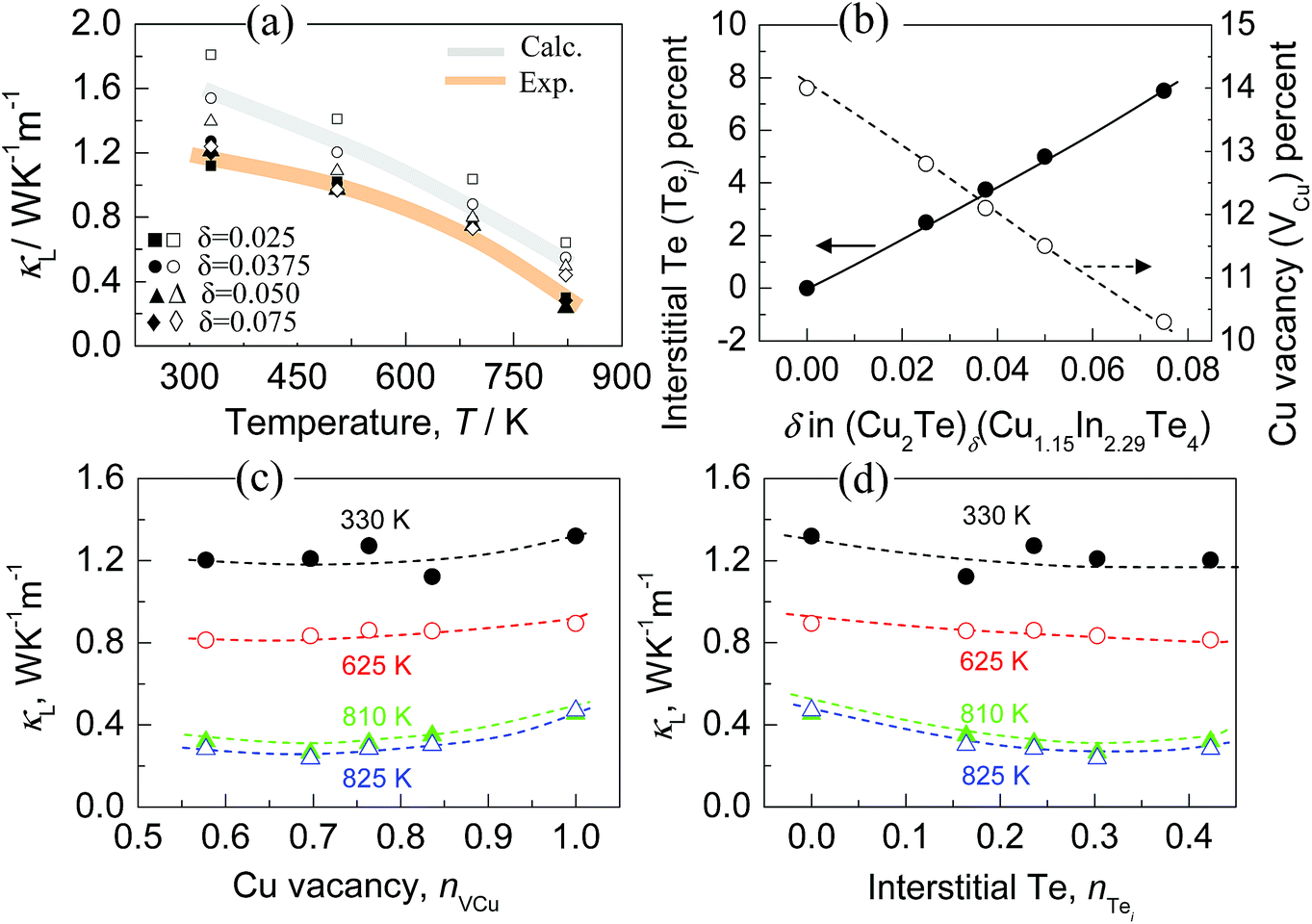 | ||
| Fig. 6 (a) Comparison of the calculated lattice thermal conductivities (calc.) with those of experimental counterparts (exp.); (b) copper vacancy (VCu) and interstitial Te (Tei) percentages as a function of Cu2Te content (δ value); (c) lattice thermal conductivities (κL) at 330 K, 625 K, 810 K and 825 K as a function of nVCu (ratio of the copper vacancies to total defect concentrations); (d) lattice thermal conductivities (κL) at 330 K, 625 K, 810 K and 825 K as a function of nTei (ratio of the interstitial Te to total defect concentrations). | ||
4.5 The phonon dispersion
Next to further justify the aforementioned qualitative understanding of the lattice dynamics, we have calculated the phonon dispersions for Cu20In40Te72 and Cu22In40Te73. Fig. 7a and b show the phonon dispersions for the pristine (Fig. 7a) and doped (Fig. 7b) system corresponding to δ = 0.05, and Fig. 7c a corresponding zoomed view near the lower frequency range. We see an overall shift in the frequency towards lower values after doping. This can be understood as the effect of bond weakening because of the interstitial dopants. Near the frequency window of 10–20 cm−1, new rattling modes are introduced after doping. This can much clearly be seen in the difference spectra (Fig. 7d) calculated from the phonon DOS of both the structures. The hybridization between the newly introduced rattling modes due to the interstitial dopants with the acoustic branches therefore promotes the scattering of phonons, resulting in lower κL values in the doped system.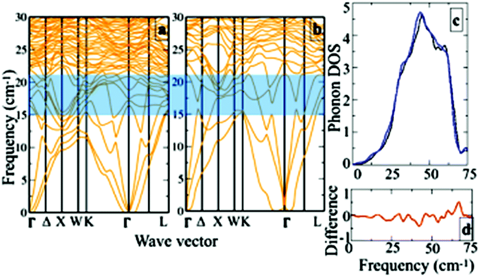 | ||
| Fig. 7 The phonon dispersion for (a) pristine (corresponding to Cu20In40Te72) and (b) doped system for δ = 0.05 (corresponding to Cu22In40Te73). (c) The zoomed view near the lower frequency range and (d) their difference spectra. | ||
5. Conclusions
In summary, Cu-deficient (Cu2Te)δ(Cu1.15In2.29Te4) (δ = 0, 0.025, 0.0375, 0.05, 0.075) samples are prepared, and their structures and TE properties have been investigated. The first-principles calculation reveals that the creation of the resonant states at the Fermi level and impurity levels near the valence band edge increases the Seebeck coefficients and Hall carrier concentration simultaneously. Furthermore, the extra Te prefers the interstitial sites as Cu1.15In2.29Te4 is alloyed with Cu2Te. This atomic arrangement in the doped system yields a significant lattice disorder. The reduction in the lattice thermal conductivity in the doped sample (with δ = 0.05) is mainly governed by the hybridization of localized modes of the interstitial Te with the acoustic modes of stoichiometric Te and In. Consequently, the TE performance of pristine Cu1.15In2.29Te4 gets two-fold enhanced upon appropriate Cu2Te doping giving rise to the highest ZT value of ∼1.0 at 825 K.Conflicts of interest
There are no conflicts of interest to declare.Acknowledgements
This work is supported by the National Natural Science Foundation of China (51671109, 51171084, and 51575514). Open Access funding provided by the Max Planck Society.References
- W. Zhao, Z. Liu, Z. Sun, Q. Zhang, P. Wei, X. Mu, H. Zhou, C. Li, S. Ma, D. He, P. Ji, W. Zhu, X. Nie, X. Su, X. Tang, B. Shen, X. Dong, J. Yang, Y. Liu and J. Shi, Nature, 2017, 549, 247 CrossRef CAS PubMed.
- L. Zhao, G. Tan, S. Hao, J. He, Y. Pei, H. Chi, H. Wang, S. Gong, H. Xu, V. P. Dravid, C. Uher, G. J. Snyder, C. Wolverton and M. G. Kanatzidis, Science, 2016, 351, 141 CrossRef CAS PubMed.
- J. Zhang, L. Song, S. H. Pedersen, H. Yin, L. T. Hung and B. B. Iversen, Nat. Commun., 2017, 8, 13901 CrossRef CAS PubMed.
- Y. Pei, X. Shi, A. LaLonde, H. Wang, L. Chen and G. J. Snyder, Nature, 2011, 473, 66 CrossRef CAS PubMed.
- J. P. Heremans, V. Jovovic, E. S. Toberer, A. Saramat, K. Kurosaki, A. Charoenphakdee, S. Yamanaka and G. J. Snyder, Science, 2008, 321, 554 CrossRef CAS PubMed.
- S. Lin, W. Li, Z. Chen, J. Shen, B. Ge and Y. Pei, Nat. Commun., 2016, 7, 10287 CrossRef CAS PubMed.
- B. Poudel, Q. Hao, Y. Ma, Y. Lan, A. Minnich, B. Yu, X. Yan, D. Wang, A. Muto, D. Vashaee, X. Chen, J. Liu, M. S. Dresselhaus, G. Chen and Z. Ren, Science, 2008, 320, 634 CrossRef CAS PubMed.
- K. Biswas, J. He, I. D. Blum, C.-I. Wu, T. P. Hogan, D. N. Seidman, V. P. Dravid and M. G. Kanatzidis, Nature, 2012, 489, 414 CrossRef CAS PubMed.
- H. Liu, X. Shi, F. Xu, L. Zhang, W. Zhang, L. Chen, Q. Li, C. Uher, T. Day and G. J. Snyder, Nat. Mater., 2012, 11, 422 CrossRef CAS PubMed.
- H. Liu, X. Yuan, P. Lu, X. Shi, F. Xu, Y. He, Y. Tang, S. Bai, W. Zhang, L. Chen, Y. Lin, L. Shi, H. Lin, X. Gao, X. Zhang, H. Chi and C. Uher, Adv. Mater., 2013, 25, 6607 CrossRef CAS PubMed.
- L.-D. Zhao, S.-H. Lo, Y. Zhang, H. Sun, G. Tan, C. Uher, C. Wolverton, V. P. Dravid and M. G. Kanatzidis, Nature, 2014, 508, 373 CrossRef CAS PubMed.
- P. Ying, X. Li, Y. Wang, J. Yang, C. Fu, W. Zhang, X. Zhao and T. Zhu, Adv. Funct. Mater., 2017, 27, 1604145 CrossRef.
- W. Li, S. Lin, B. Ge, J. Yang, W. Zhang and Y. Pei, Adv. Sci., 2016, 3, 1600196 CrossRef PubMed.
- S. Lin, W. Li, S. Li, X. Zhang, Z. Chen, Y. Xu, Y. Chen and Y. Pei, Joule, 2017, 1, 816 CrossRef CAS.
- Y. Pei, L. Zheng, W. Li, S. Lin, Z. Chen, Y. Wang, X. Xu, H. Yu, Y. Chen and B. Ge, Adv. Electron. Mater., 2016, 2, 1600019 CrossRef.
- W. Li, L. Zheng, B. Ge, S. Lin, X. Zhang, Z. Chen, Y. Chang and Y. Pei, Adv. Mater., 2017, 29, 1605887 CrossRef PubMed.
- L. Zheng, W. Li, S. Lin, J. Li, Z. Chen and Y. Pei, ACS Energy Lett., 2017, 2, 563 CrossRef CAS.
- J. Li, X. Zhang, S. Lin, Z. Chen and Y. Pei, Chem. Mater., 2017, 29, 605 CrossRef CAS.
- V. Zaitsev, M. Fedorov, E. Gurieva, I. Eremin, P. Konstantinov, A. Y. Samunin and M. Vedernikov, Phys. Rev. B: Condens. Matter Mater. Phys., 2006, 74, 045207 CrossRef.
- G. Tan, W. G. Zeier, F. Shi, P. Wang, G. J. Snyder, V. P. Dravid and M. G. Kanatzidis, Chem. Mater., 2015, 27, 7801 CrossRef CAS.
- J. Shen, X. Zhang, S. Lin, J. Li, Z. Chen, W. Li and Y. Pei, J. Mater. Chem. A, 2016, 4, 15464 RSC.
- W. Li, S. Lin, X. Zhang, Z. Chen, X. Xu and Y. Pei, Chem. Mater., 2016, 28, 6227 CrossRef CAS.
- J. Cui, J. Zhu, Z. Han and Y. Luo, J. Mater. Chem. A, 2018, 6, 12672 RSC.
- X. Zhang, Z. Chen, S. Lin, B. Zhou, B. Gao and Y. Pei, ACS Energy Lett., 2017, 2, 2470 CrossRef CAS.
- J. Li, H. Wu, D. Wu, C. Wang, Z. Zhang, Y. Li, F. Liu, W. Ao and J. He, Chem. Mater., 2016, 28, 6367 CrossRef CAS.
- G. Tan, S. Hao, J. Zhao, C. Wolverton and M. G. Kanatzidis, J. Am. Chem. Soc., 2017, 139, 6467 CrossRef CAS PubMed.
- Y. Luo, J. Yang, Q. Jiang, W. Li, D. Zhang, Z. Zhou, Y. Cheng, Y. Ren and X. He, Adv. Energy Mater., 2016, 6, 1600007 CrossRef.
- Y. Luo, Q. Jiang, J. Yang, W. Li, D. Zhang, Z. Zhou, Y. Cheng, Y. Ren, X. He and X. Li, Nano Energy, 2017, 32, 80 CrossRef CAS.
- H. Yu, L. Chen, H. Pang, X. Qin, P. Qiu, X. Shi, L. Chen and X. Chen, Materials Today Physics, 2018, 5, 1 CrossRef.
- G. Zhou and D. Wang, Phys. Chem. Chem. Phys., 2016, 18, 5925 RSC.
- H. Chen, C. Yang, H. Liu, G. Zhang, D. Wan and F. Huang, CrystEngComm, 2013, 15, 6648 RSC.
- J. Zhu, Y. Luo, G. Cai, X. Liu, Z. Du, F. Tang and J. Cui, J. Mater. Chem. A, 2017, 5, 24199 RSC.
- A. Kosuga, T. Plirdpring, R. Higashine, M. Matsuzawa, K. Kurosaki and S. Yamanaka, Appl. Phys. Lett., 2012, 100, 042108 CrossRef.
- A. Yusufu, K. Kurosaki, A. Kosuga, T. Sugahara, Y. Ohishi, H. Muta and S. Yamanaka, Appl. Phys. Lett., 2011, 99, 061902 CrossRef.
- M. Zebarjadi, B. Liao, K. Esfarjani, M. Dresselhaus and G. Chen, Adv. Mater., 2013, 25, 1577 CrossRef CAS PubMed.
- J. Yang, S. Chen, Z. Du, X. Liu and J. Cui, Dalton Trans., 2014, 43, 15228 RSC.
- H. Kim, Z. M. Gibbs, Y. Tang, H. Wang and G. J. Snyder, APL Mater., 2015, 3, 041506 CrossRef.
- V. Blum, R. Gehrke, F. Hanke, P. Havu, V. Havu, X. Ren, K. Reuter and M. Scheffler, Comput. Phys. Commun., 2009, 180, 2175 CrossRef CAS.
- P. Hohenberg and W. Kohn, Phys. Rev., 1964, 136, B864 CrossRef.
- J. P. Perdew, K. Burke and M. Ernzerhof, Phys. Rev. Lett., 1996, 77, 3865 CrossRef CAS.
- A. V. Krukau, O. A. Vydrov, A. F. Izmaylov and G. E. Scuseria, J. Chem. Phys., 2006, 125, 224106 CrossRef PubMed.
- A. Togo, F. Oba and I. Tanaka, Phys. Rev. B, 2008, 78, 134106 CrossRef.
- D. Zhang, J. Yang, Q. Jiang, Z. Zhou, X. Li, J. Xin, A. Basit, Y. Ren and X. He, Nano Energy, 2017, 36, 156 CrossRef CAS.
- Z. Zhao, X. He, J. Yi, C. Ma, Y. Cao and J. Qiu, RSC Adv., 2013, 3, 84 RSC.
- J. P. Heremans, B. Wiendlocha and A. M. Chamoire, Energy Environ. Sci., 2012, 5, 5510 RSC.
- B. Wiendlocha, J.-B. Vaney, C. Candolfi, A. Dauscher, B. Lenoir and J. Tobola, Phys. Chem. Chem. Phys., 2018, 20, 12948 RSC.
- L. Zhang, Q. Zheng, Y. Xie, Z. Lan, O. V. Prezhdo, W. A. Saidi and J. Zhao, Nano Lett., 2018, 18, 1592 CrossRef CAS PubMed.
- G. J. Snyder and E. S. Toberer, Nat. Mater., 2008, 7, 105 CrossRef CAS PubMed.
- N. Cheng, R. Liu, S. Bai, X. Shi and L. Chen, J. Appl. Phys., 2014, 115, 163705 CrossRef.
- R. Liu, Y. Qin, N. Cheng, J. Zhang, X. Shi, Y. Grin and L. Chen, Inorg. Chem. Front., 2016, 3, 1167 RSC.
- E. Guedez, C. Rincón, S. M. Wasim, G. E. Delgado, G. Marcano and G. Sánchez-Pérez, Phys. Status Solidi B, 2017, 254, 1700087 CrossRef.
- H. Chen, C. Yang, H. Liu, G. Zhang, D. Wan and F. Huang, CrystEngComm, 2013, 15, 6648 RSC.
- R. Liu, L. Xi, H. Liu, X. Shi, W. Zhang and L. Chen, Chem. Commun., 2012, 48, 3818 RSC.
- Z. Xia, G. Wang, X. Zhou and W. Wen, Ceram. Int., 2017, 43, 16276 CrossRef CAS.
- S. Roychowdhury, M. K. Jana, J. Pan, S. N. Guin, D. Sanyal, U. V. Waghmare and K. Biswas, Angew. Chem., Int. Ed., 2018, 57, 4043 CrossRef CAS PubMed.
- Y. Shi, A. Assoud, S. Ponou, S. Lidin and H. Kleinke, J. Am. Chem. Soc., 2018, 140, 8578 CrossRef CAS PubMed.
- Y. Bouyrie, C. Candolfi, A. Dauscher, B. Malaman and B. Lenoir, Chem. Mater., 2015, 27, 8354 CrossRef CAS.
- C. Lin, R. Lydia, J. Yun, H. Lee and J. Rhyee, Chem. Mater., 2017, 29, 5344 CrossRef CAS.
- J. Callaway and H. C. Von Baeyer, Phys. Rev., 1960, 120, 1149 CrossRef CAS.
- W. Yao, D. Yang, Y. Yan, K. Peng, H. Zhan, A. Liu, X. Lu, G. Wang and X. Zhou, ACS Appl. Mater. Interfaces, 2017, 9, 10595 CrossRef CAS PubMed.
- K. Kurosaki, H. Matsumoto, A. Charoenphakdee, S. Yamanaka, M. Ishimaru and Y. Hirotsu, Appl. Phys. Lett., 2008, 93, 012101 CrossRef.
- C. Kim, K. Kurosaki, M. Ishimaru, H. Muta and S. Yamanaka, J. Electron. Mater., 2011, 40, 999 CrossRef CAS.
- T. Plirdpring, K. Kurosaki, A. Kosuga, M. Ishimaru, A. Harnwunggmoung, T. Sugahara, Y. Ohishi, H. Muta and S. Yamanaka, Appl. Phys. Lett., 2011, 98, 172104 CrossRef.
Footnote |
| † Electronic supplementary information (ESI) available. See DOI: 10.1039/c8ta10741f |
| This journal is © The Royal Society of Chemistry 2019 |