
12.88% efficiency in doctor-blade coated organic solar cells through optimizing the surface morphology of a ZnO cathode buffer layer†
Guoqi
Ji
ad,
Wenchao
Zhao
c,
Junfeng
Wei
a,
Lingpeng
Yan
a,
Yunfei
Han
a,
Qun
Luo
 *abe,
Shangfeng
Yang
d,
Jianhui
Hou
*c and
Chang-Qi
Ma
*ab
*abe,
Shangfeng
Yang
d,
Jianhui
Hou
*c and
Chang-Qi
Ma
*ab
aSuzhou Institute of Nano-Tech and Nano-Bionics, Printable Electronics Research Center (SINANO), Chinese Academy of Sciences, Collaborative Innovation Center of Suzhou Nano Science and Technology, Suzhou, Jiangsu 215123, P. R. China. E-mail: qluo2011@sinano.ac.cn
bCollege of Nano-Tech and Nano-Bionics, University of Science and Technology of China, Hefei, 230027, P. R China
cInstitute of Chemistry, Chinese Academy of Sciences, Beijing, 100190, P. R. China
dNano Science and Technology Institute, University of Science and Technology of China, 166 Ren Ai Road, SEID SIP, Suzhou, Jiangsu 215123, P. R. China
eState Key Lab of Silicon Materials, Zhejiang University, Hangzhou, 310027, P.R. China
First published on 4th December 2018
Abstract
Doctor-blade coating (DBC) is a roll-to-roll compatible high-throughput thin film fabrication route with little solution wastage and is considered as a more scalable method for the fabrication of organic solar cells (OSCs) than spin coating (SC). Since wet film drying is much slower during DBC than during SC, the interfacial connection within the films might be different, which could remarkably influence the device performance of OSCs. In this work, we demonstrated that the device performance, reproducibility, and long-term stability are more sensitive to the ZnO morphology in doctor-blade (DB)-coated cells than in spin-coated cells in both fullerene (PTB7-Th:PC71BM) and non-fullerene (PBDB-TF:IT-4F) systems. Such an influence is more significant in large-area cells. We ascribe this enormous difference between the spin-coated and DB-coated devices to different interfacial contacts, which were caused by different spreading forces and drying kinetics during the thin film formation process. A smooth ZnO cathode buffer layer from methanol-dispersed inks was more suitable for DBC, and with this layer, a high power conversion efficiency of 12.88% and 9.22% was achieved for the 0.12 and 1.04 cm2 DB-coated PBDB-TF:IT-4F OSCs, respectively.
Introduction
Bulk heterojunction (BHJ) organic solar cells (OSCs) have been extensively developed by designing and synthesizing novel photoactive materials, optimizing electrode buffer layers, controlling the film morphology1–3 and controlling the device fabrication process. Currently, high power conversion efficiencies (PCEs) over 17% have been achieved for small-area devices.4 In addition to the advantages of lowcost and mechanical flexibility, OSCs also have great potential to be fabricated via high-throughput printing techniques, such as doctor-blade coating (DBC),5–8 ink-jet printing,9,10 slot die coating,11,12 and other printing methods.13 In the field of printed photovoltaics, there are many technology issues that should be solved before the transformation from lab to fab to industrialization; these issues include regulating the solvent and additives,14 controlling the film morphology,15 developing new transparent conductive electrodes,16,17 and modifying the electrode interface.18 Currently, increasingly more studies have been focused on active film morphology regulation through using green solvents and suitable additives as well as optimizing the processing conditions.15,19 In addition to the active layer, it is well known that the electrode buffer layers also significantly influence the film morphology, phase separation,20 interfacial contact,19,21,22 and finally the device performance. Therefore, many research efforts have been devoted to improving the device performance through interface engineering. However, most of them were for the cells fabricated from spin coating (SC), and few efforts have been made to optimize the interfaces for printed photovoltaics to the best of our knowledge. We know that a roll-to-roll (R2R) printer can fabricate several kilometres of cell modules in over a few hours.23–26 In addition, the drying kinetics and suitable ink formulations for R2R printing and SC are quite different.14,27 Therefore, the bottom interface properties, including the surface energy, surface roughness and film morphology, might have a more profound influence on the device performance.As for the electrode buffer layer, zinc oxide (ZnO) is the most widely used cathode buffer layer (CBL) in inverted OSCs because of its high electron mobility, high visible transparency, ease of fabrication, and environmental friendliness.28 Additionally, ZnO has been considered as the most promising CBL for R2R printed devices to date.29 A variety of synthesis approaches28,30 and modification routes18,31–33 have been developed to prepare an excellent ZnO CBL for OSCs; these diverse synthesis approaches have caused a large inherent difference in the film morphology and photoelectrical properties of ZnO layers. As a typical example, Liang et al.34 and Ma et al.35 found that the ZnO surface morphology could greatly influence the interfacial contact between the CBL and the photoactive layer due to the surface energy difference between ZnO and the active layer.34 Li et al. found that the solvent significantly influences the aggregation and dispersion of ZnO nanoparticles and subsequently influences the device performance.36 However, most of these studies have focused on conventional spin-coated devices; the issue concerning the influence of the ZnO CBL on the performance of the R2R printed device has rarely been reported to our knowledge. In this study, we used DBC and SC as research models to comprehensively compare the influence of the bottom buffer layer on the device performance. Two kinds of ZnO CBLs with different surface roughnesses were fabricated from acetone- and methanol-based ZnO inks. Our results demonstrated that a slight morphology difference in the ZnO CBLs caused a minor variation in the device performance, performance homogeneity, and long-term stability of the spin-coated device. However, for the doctor-blade (DB)-coated device, a slight morphology difference of ZnO CBLs resulted in obvious differences in the device performance, particularly the reproducibility. In this work, a smoother ZnO buffer layer fabricated from methanol-based inks can benefit the interfacial contact between the CBL and the organic photoactive layer, and consequently contribute to the higher performance, narrower performance distribution, and longer lifetime for the DB-coated devices. With this smoother ZnO layer, a record performance of 12.88% with good reproducibility was achieved via DBC, which is the highest value in the reported work. In addition, this work provides significant guidance that the influence of surface morphology and roughness of the bottom buffer layer on the photovoltaic performance and process reproducibility should be highly evaluated in printed organic photovoltaics.
Results and discussion
Inverted OSCs with an architecture of indium-tin oxide (ITO)/ZnO/donor:acceptor/MoO3/Al were prepared, where PTB7-Th:PC71BM and PBDB-TF:IT-4F heterojunctions were selected as the modules of the fullerene and non-fullerene photoactive layers, respectively. The chemical structures of PTB7-Th, PC71BM, PBDB-TF and IT-4F, as well as the molecular energy level diagram of the inverted OSCs, are shown in Fig. 1. Two kinds of ZnO films fabricated from acetone (A-ZnO) and methanol (M-ZnO) inks were used as the CBLs. The active layers were deposited on top of the A-ZnO or M-ZnO CBLs through both SC and DBC. First, the particle diameters of the A-ZnO and M-ZnO nanoparticles were recorded by dynamic light scattering (DLS, as shown in Fig. S1†). One can see that the A-ZnO and M-ZnO nanoparticles have similar size distributions with average diameters of 13.5 and 12.6 nm, respectively. Since the crystal sizes of the ZnO nanoparticles were approximately 5–8 nm,37 DLS results suggested that the ZnO nanoparticles were dispersible in both acetone and methanol without serious aggregation. However, the A-ZnO and M-ZnO films showed different morphologies. The scanning electron microscopy (SEM) images showed that the A-ZnO film was loose and inhomogeneous with obvious voids, while the M-ZnO film was compact and homogeneous. According to the atomic force microscopy (AFM) images, the root mean square (RMS) roughness values of the A-ZnO and M-ZnO films were 4.24 and 1.89 nm, respectively. Since the A-ZnO and M-ZnO nanoparticles do not show obvious differences in solution, the rougher surface of the A-ZnO films could be ascribed to the faster drying process of the acetone-based inks. As shown in the images of a water droplet on top of the A-ZnO and M-ZnO films, the contact angles of water on the A-ZnO and M-ZnO films were 24° and 34°, respectively. The larger contact angle between the M-ZnO films and water might lead to improved contact between the CBL and the organic photoactive solution.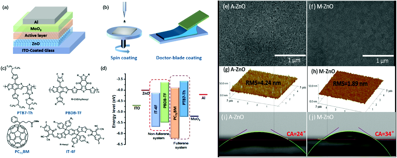 | ||
| Fig. 1 (a) Schematic illustration of the device architecture of the inverted OSCs. (b) Schematic diagram of the SC and DBC processes. (c) Molecular structures of PTB7-Th, PC71BM, PBDB-TF and IT-4F. (d) The energy level diagram of the inverted OSCs. SEM and AFM images of the ZnO films fabricated from acetone (A-ZnO (e, g)) and methanol (M-ZnO (f, h)) solvents. The contact angle between the (i) A-ZnO and (j) M-ZnO films and water. | ||
The widely studied PTB7-Th:PC71BM was used as the photoactive layer for cell fabrication. The current density–voltage (J–V) curves and the external quantum efficiency (EQE) spectra of the optimized devices are shown in Fig. 2, and the performance parameters are listed in Table 1. As can be seen from Table 1, the spin-coated devices with the A-ZnO and M-ZnO CBLs presented similar performances with a power conversion efficiency (PCE) of approximately 9.0%. In addition, these devices had similar statistical deviations of approximately 0.06%. This result revealed that the performance of the spin-coated small-area device is less dependent on the morphology of the bottom buffer layers. However, surprisingly, the DB-coated devices showed larger differences both in the optimized performance and performance homogeneity. Specifically, the A-ZnO CBL-based device exhibited an average PCE of 8.25% and a relatively large standard deviation of 0.47%, while the device with the M-ZnO CBL showed a higher average PCE of 8.98% and a lower standard deviation of 0.23%. This result demonstrated that the surface morphology of the ZnO CBL would greatly affect the device performance of the DB-coated devices, and a smooth ZnO CBL is essential for high performance of the DB-coated OSCs, which was attributed to the interfacial charge transport properties between the CBL and the organic active layer (vide infra). From the histogram of the performance parameters (Fig. S2†), we found that the larger performance difference between the A-ZnO and M-ZnO CBL-based DB-coated solar cells was mainly due to the fill factor (FF) rather than open-circuit voltage (VOC) and short-circuit current density (JSC). With a smooth M-ZnO CBL, a FF of 69% was achieved for the DB-coated OSCs, which was nearly comparable to that of the spin-coated cells, while when a rough A-ZnO CBL was used in the DB-coated OSCs, the FF was relatively low (66%). Besides this, the histogram of FF (as shown in Fig. S2(a)†) revealed that the M-ZnO CBL-based DB cells gave a much smaller variation than the A-ZnO CBL-based devices. For the M-ZnO CBL-based device, the FF varied from 66% to 70%, showing a small deviation. In contrast, the FF of the A-ZnO CBL-based device varied from 62% to 69%. Such a remarkably improved FF finally resulted in enhanced device performance. In addition, as indicated by the series (Rs) and shunt resistance (Rsh) of the devices, it was found that the A-ZnO CBL based DB-coated cells have larger Rs and smaller Rsh than other devices, which should be the main reason for the lower FF.
 | ||
| Fig. 2 (a) J–V characterization, (b) EQE spectra, and (c,d) the performance distribution of the PTB7-Th:PC71BM devices fabricated via SC and DBC. (e) J–V characterization, (f) EQE spectra, and (g, h) the performance distribution of the PBDB-TF:IT-4F devices fabricated via SC and DBC. | ||
| Entry | Active layer | Process | ZnO films | V OC (V) | J SC (mAcm−2) | FF (%) | PCE (%) | Ave. PCE ± std. dev. (%)a | R s (Ωcm2) | R sh (Ωcm2) |
|---|---|---|---|---|---|---|---|---|---|---|
| a Average performance calculated over 12 individual devices. | ||||||||||
| 1 | PTB7-Th:PC71BM | SC | A | 0.79 | 16.24 | 70 | 9.01 | 8.93±0.06 | 6.12 | 1877 |
| 2 | M | 0.79 | 16.91 | 69 | 9.22 | 9.12±0.07 | 5.64 | 1601 | ||
| 3 | PTB7-Th:PC71BM | DBC | A | 0.79 | 16.73 | 66 | 8.72 | 8.25±0.47 | 6.39 | 1642 |
| 4 | M | 0.79 | 16.37 | 69 | 9.33 | 8.98±0.13 | 5.93 | 2814 | ||
| 5 | PBDB-TF:IT-4F | SC | A | 0.86 | 20.30 | 71 | 12.40 | 12.22±0.19 | 5.48 | 1977 |
| 6 | M | 0.86 | 20.79 | 72 | 12.81 | 12.50±0.18 | 4.59 | 2118 | ||
| 7 | PBDB-TF:IT-4F | DBC | A | 0.86 | 20.09 | 68 | 11.74 | 11.22±0.53 | 6.27 | 1107 |
| 8 | M | 0.86 | 20.80 | 72 | 12.88 | 12.34±0.21 | 4.46 | 1959 | ||
To further investigate the influence of the ZnO buffer layer on the performance of OSCs and achieve high performance for the DB-coated cells, the high efficiency non-fullerene acceptor heterojunction system PBDB-TF:IT-4F![[thin space (1/6-em)]](https://www.rsc.org/images/entities/char_2009.gif) 38 was selected as the photoactive layer, and the organic active layers were fabricated through both SC and DBC. The main performance parameters of the PBDB-TF:IT-4F cells are also summarized in Table 1. As shown in Table 1, the highest performance and the standard deviations of the A-ZnO and M-ZnO CBL-based devices were similar for the spin-coated cells. Again, we found that the performance of the spin-coated cells was less sensitive to the ZnO CBL, which was similar to the results of the PTB7-Th:PC71BM devices. However, for the DB-coated devices, the overall performance, including the optimized performance and the performance distribution uniformity of the A-ZnO CBL-based devices, was poorer than that of the M-ZnO CBL-based devices. Though the PCE of the A-ZnO CBL-based spin-coated device reached above 12.5%, the DB-coated device with the same A-ZnO CBL gave a PCE of 11.22%. Meanwhile, the deviation (0.53%) was much larger than that of the spin-coated devices (0.21%). Nevertheless, the performance of the M-ZnO CBL-based DB-coated cells was obviously improved, which exhibited an average PCE of 12.34% and a deviation of 0.21%. And the optimized performance of the 0.12 cm2 device reached 12.88%, which was nearly the highest PCE for the DB-coated OSCs.39–42 Similar to the PTB7-Th:PC71BM solar cells, the performance variation between the A-ZnO and M-ZnO devices was also mainly caused by the FF.
38 was selected as the photoactive layer, and the organic active layers were fabricated through both SC and DBC. The main performance parameters of the PBDB-TF:IT-4F cells are also summarized in Table 1. As shown in Table 1, the highest performance and the standard deviations of the A-ZnO and M-ZnO CBL-based devices were similar for the spin-coated cells. Again, we found that the performance of the spin-coated cells was less sensitive to the ZnO CBL, which was similar to the results of the PTB7-Th:PC71BM devices. However, for the DB-coated devices, the overall performance, including the optimized performance and the performance distribution uniformity of the A-ZnO CBL-based devices, was poorer than that of the M-ZnO CBL-based devices. Though the PCE of the A-ZnO CBL-based spin-coated device reached above 12.5%, the DB-coated device with the same A-ZnO CBL gave a PCE of 11.22%. Meanwhile, the deviation (0.53%) was much larger than that of the spin-coated devices (0.21%). Nevertheless, the performance of the M-ZnO CBL-based DB-coated cells was obviously improved, which exhibited an average PCE of 12.34% and a deviation of 0.21%. And the optimized performance of the 0.12 cm2 device reached 12.88%, which was nearly the highest PCE for the DB-coated OSCs.39–42 Similar to the PTB7-Th:PC71BM solar cells, the performance variation between the A-ZnO and M-ZnO devices was also mainly caused by the FF.
As previously mentioned, it is interesting to find that both the performance and performance uniformity of the DB-coated devices are more sensitive to the ZnO CBLs. Such performance variation is mainly caused by the FF rather than VOC or JSC. To exclude the influence of the photoactive layer, AFM images and absorption spectra of the active layers on different ZnO CBLs were recorded. From the AFM images, we observed that the active layers on A-ZnO and M-ZnO exhibited similar surface roughnesses (Fig. S3†). In addition, the two films also presented nearly the same absorption spectra, proving that these active layers had similar film thicknesses (see the ESI, Fig. S4†). Therefore, we speculated that the difference in device performance was not caused by the thickness variation of the photoactive layers. As for the interfacial properties, we know that both the photoelectrical properties of the buffer layers and the interfacial contact between buffer layers and the organic photoactive layer would affect the device performance. Herein, since the spin-coated devices with different A-ZnO and M-ZnO CBLs gave similar device performance parameters, i.e., VOC, JSC, FF, and PCE, this indicated that the electrical properties of the A-ZnO and M-ZnO films were not considerably impacted by surface roughness. Therefore, the performance variation in the DB-coated devices could not be ascribed to the electrical properties of the ZnO layers but possibly to the interface charge transport properties between the CBL and the organic active layer.
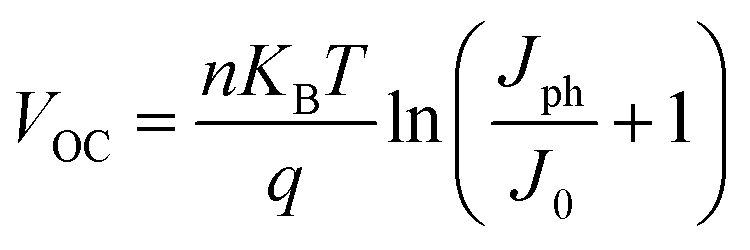
The light intensity-dependent J–V characteristics of the spin-coated and DB-coated devices were further measured to study the trap states in these different devices. Fig. 3(a) and (b) show the JSC and VOC of these cells measured under different light intensities. First, the JSC is incident light intensity-dependent with a relationship of J∝Iα, where α typically ranges from 0.85 to 1 for polymer solar cells. The deviation from α = 1 was ascribed to a small loss of carriers via bimolecular recombination and space charge effects.43,44 Herein, JSC was linearly correlated with the light intensity with a slope (α) of approximately 0.920 for all the devices, suggesting that bimolecular charge recombination and space charge effects are negligible for both the spin-coated and the DB-coated devices.45,46 From the VOCvs. light intensity curves, we found that there were obvious differences in the devices fabricated via the different methods and based on different ZnO CBLs. According to the literature, the VOC is determined by the difference in the rates of charge generation and charge recombination.47 For ideal p–n junction solar cells, the VOC can be described by the following equation:48
 | (1) |
 | ||
| Fig. 3 Light intensity dependence of the (a) JSC and (b) VOC of the PBDB-TF:IT-4F devices. (c) Electrochemical impedance spectra of the devices. | ||
The electrochemical impedance spectra (EIS) of these devices were measured in the dark to analyse the series resistances. As shown in the Nyquist plots of these devices in Fig. 3(c), we found that all the plots exhibited asymmetric semicircles and could be fitted with an equivalent circuit model (as shown in the inset of Fig. 3(c)) that comprised three resistances Rs, R1, and R2 and two capacitances C1 and C2. Using this module, detailed results of Rs, R1, and R2 were calculated and are shown in Table S1.† The results showed that Rs and R1 were nearly the same in these devices, while a large difference in R2 could be found among these devices. Therefore, Rs and R1 might be ascribed to the resistance of the system and the bulk heterojunction, respectively, and R2 could be attributed to the chemical resistance caused by the contact properties between the active layer and the ZnO CBL. Similar electrochemical impedance spectra have been reported by Wang et al.50 for inverted OSCs. Herein, the smaller R2 in the spin-coated cells than in the DB-coated cells indicated better interfacial contact for devices fabricated through SC. The observation of a very high R2 in the A-ZnO based DB-coated cells indicated a significantly poor interfacial contact, which was in good agreement with the device performance.
To better understand the reason for the ZnO-dependent performance homogeneity, laser beam-induced current (LBIC) mapping images of these devices were recorded, and a laser beam with a wavelength of 532 nm was used as the illumination source. Photocurrent mapping images of the devices were recorded via line scanning along the scan direction of both X and Y, and finally some colourful regions corresponding to relatively weak and strong photocurrent regions could be found. The device performances of the A-ZnO SC, M-ZnO SC, A-ZnO DBC, and M-ZnO DBC devices used for the LBIC mapping are listed in Table S2.† From Fig. 4(a–d), it was found that the A-ZnO SC, M-ZnO SC and M-ZnO DBC devices showed homogeneous current distribution. However, the current mapping image of the A-ZnO CBL-based DB-coated device contained some low current regions. Such a non-uniform LBIC distribution in the A-ZnO CBL-based DB-coated device might be ascribed to the relatively poor interfacial contact between the A-ZnO CBL and the DBC active layers.
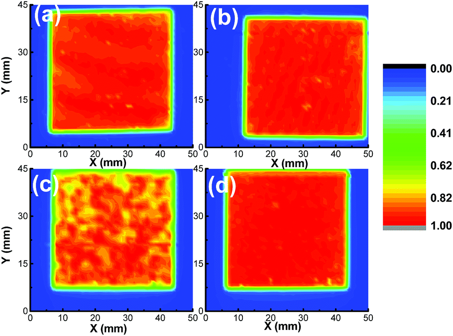 | ||
| Fig. 4 LBIC mapping of the spin-coated and DB-coated PBDB-TF:IT-4F devices: (a) A-ZnO/SC, (b) M-ZnO/SC, (c) A-ZnO/DBC, and (d) M-ZnO/DBC. | ||
On the basis of the above observations, we can make a conclusion that the higher sensitivity of the device performance and performance homogeneity to the ZnO buffer layer both for the DB-coated fullerene and non-fullerene devices relative to that of the spin-coated device could be due to the interfacial contact. Such a considerable difference could be further attributed to the different spreading forces and drying kinetics for these two different deposition technologies. As we know, the precursor inks of the photoactive layer are spread out through continuous centrifugal forces during SC, and thus, the photoactive precursor solution could effectively spread out on the surface of the bottom buffer layer and subsequently form a homogeneous film, whether the surface roughness of the bottom buffer layer is 1.89 or 4.24 nm. In contrast, the ink droplet spreads out under the shear force of the blade during the DBC process. Since shear forces are much milder than centrifugal forces, the mild spreading force during the DBC process can lead to inferior interfacial contact. In addition, another possible reason is the different drying dynamic kinetics of the SC and DBC processes. As we know, SC and DBC of the same ink formulation at the same temperature will favor faster drying during SC. However, during the DBC process, the solution droplet might tend to shrink naturally during the slow drying process51,52 and consequently form a poor interfacial contact. Under these circumstances, the photoactive layer morphology, film roughness, and especially the interfacial contact would be greatly impacted by the bottom CBL in the case of DBC. The M-ZnO CBL with a smooth and homogeneous ZnO surface will allow intimate contact with the photoactive blend layer, therefore leading to improved performance and less performance deviation. Fig. 5 shows the simplified schematic diagram of the traditional SC and printing processes on the A-ZnO and M-ZnO CBLs. We can see that good interfacial contact could be obtained with either a relatively smooth ZnO or a rough ZnO CBL in the spin-coated devices due to the larger spreading force and appropriate drying dynamic kinetics. However, for the DB-coated devices, an inferior interfacial contact could be formed when using a rough ZnO CBL since the active layer would not be well spread on the rough surface. Based on this result, it is also reasonable to speculate that the bottom electrode buffer layer would play a more significant role in the device performance and performance reproducibility during large-area R2R printing processes, since the R2R process is very fast.
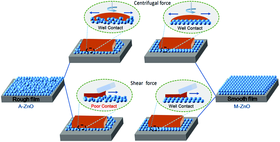 | ||
| Fig. 5 The schematic diagram of SC and DBC active layer on top of the A-ZnO and M-ZnO CBLs. | ||
The film uniformity, including the horizontal and vertical uniformities within multiple layers, is the greatest challenge for large-area printed photovoltaics. The horizontal uniformity influences the light absorption, and the vertical uniformity influences the interface charge transport and collection. Considering that the film uniformity is a critical issue for the scaling-up of solar cells,53 it is reasonable to speculate that the impact of the ZnO buffer layer on the device performance and performance homogeneity would be enhanced in large-area R2R-printed solar cells. Therefore, we also fabricated OSCs with areas of 0.75 and 1.04 cm2via DBC. As shown in the histogram of the device performance (Fig. S5†), we found that the average performance decreased gradually with an increase in the device area in both the A-ZnO and the M-ZnO buffer layer based devices due to the synergistic decrease in JSC and FF. However, for devices with the same size, the A-ZnO-based devices showed a lower average performance and a larger performance deviation than the M-ZnO devices. In particular, the performance of the 1.04 cm2 solar cells with the A-ZnO CBL varied from 6% to 8%, showing much poorer homogeneity than the M-ZnO-based devices. For the M-ZnO CBL based solar cells, an optimized performance of 10.03% and 9.22% was observed for the area of 0.75 and 1.04 cm2, respectively.
Finally, long-term stability of the device was also tested in our experiment. The long-term stability of the devices was tested in a N2-filled glove box under continuous illumination conditions. The evolution of VOC, JSC, FF and PCE of the unencapsulated PTB7-Th:PC71BM and PBDB-TF:IT-4F devices under continuous illumination conditions in a N2-filled glove box is shown in Fig. S6† and 6, respectively. For the PTB7-Th:PC71BM devices, we found that all the decay curves of the performance parameters (VOC, JSC, FF and PCE) revealed a fast decay process within 10 h and a slow decay process during long-time illumination. After about 950 h of decay, the device retained about 60–70% efficiency of the original performance. Additionally, the SC and DBC cells showed a similar degradation behavior. And the ZnO CBLs also presented a slight influence on the degradation process both for the spin-coated and DB-coated solar cells. However for the PBDB-TF:IT-4F solar cells, the long-term degradation behavior seems to be dependent on the fabrication process and the ZnO CBLs. Specifically, all the decay curves of the VOC, JSC, FF and PCE revealed a fast decay process within 20 h and a slow decay process during long-time illumination for these four devices. The decay trend of the VOC was much slower than that of the JSC and FF, indicating that the evolution of the active layer morphology and interface degradation contribute more to the device degradation. In comparison to the DB-coated devices, the devices fabricated via SC exhibited a slightly enhanced stability either using the A-ZnO or M-ZnO CBLs. After more than 1000 h of continuous illumination and working at the maximum power output point (mpp), the device performance retained approximately 90% and 50–75% of the initial value for the spin-coated and DB-coated devices, respectively. On one hand, these results revealed the excellent long-term stability of the PBDB-TF:IT-4F heterojunction solar cells, and on the other hand, these findings demonstrated that the degradation process was significantly impacted by the fabrication process of the active layers. Herein, the spin-coated device was more stable than the DB-coated device, which might be ascribed to the different active layer morphology degradations. Moreover, these results also showed that the ZnO CBL played a significant role in the device degradation. Similar to the ZnO CBL dependent device performance of the spin-coated and DB-coated devices, the degradation trend of these cells showed a different sensitivity to the ZnO CBL. Specifically, the spin-coated devices exhibited similar decay trends with either a smooth or a rough ZnO CBL. However, in the case of DBC, the A-ZnO-based devices decayed much faster than the M-ZnO devices, indicating that the long-term stability of the DB-coated devices was also highly dependent on the morphology of the bottom buffer layers. The above observations showed that the PBDB-TF:IT-4F devices were more sensitive to the ZnO CBL than the PTB7-Th:PC71BM cells, especially in the case of DB-coated cells. Such an interesting behavior of the two systems might be because different degradation mechanisms dominated the decay processes, i.e., the photoactive layer dominated degradation for PTB7-Th:PC71BM and the interface dominated degradation for PBDB-TF:IT-4F cells, which is reasonable since the IT-4F-based cell is intrinsically more stable.38 Though the underlying reason is not clear, this result showed that it is essential to obtain good interfacial contact between the active layer and the ZnO buffer layer to ensure long lifetime of printed solar cells.
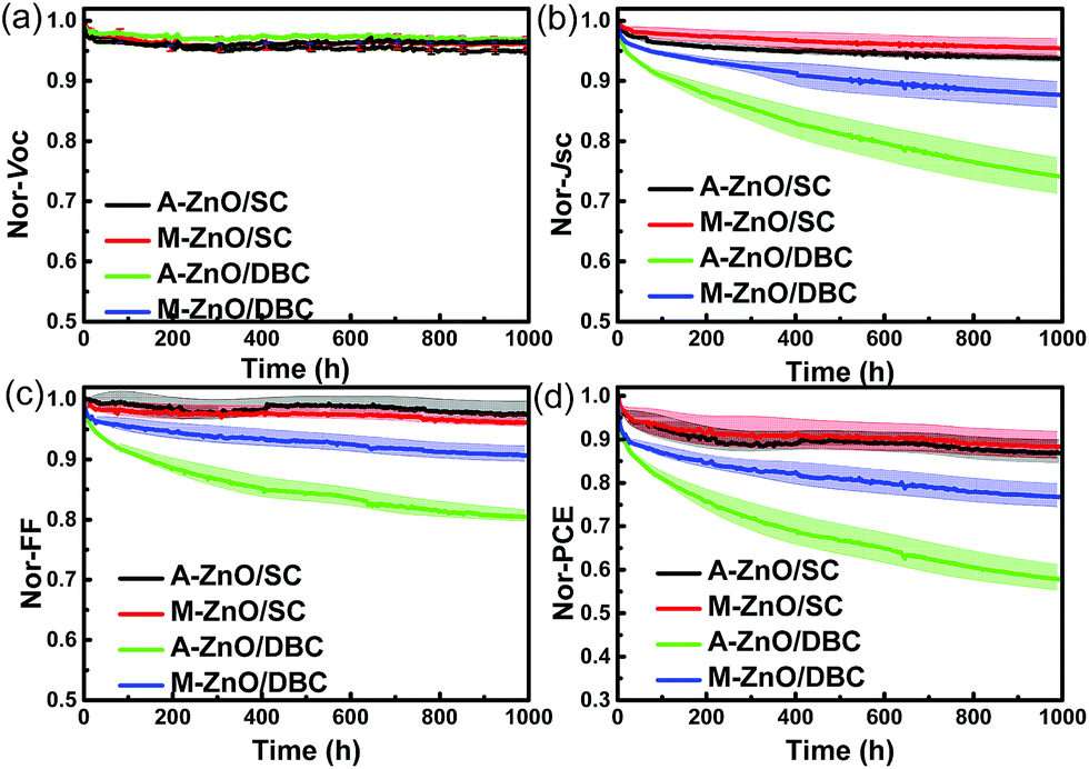 | ||
| Fig. 6 Normalized (a) VOC, (b) JSC, (c) FF, and (d) PCE decay of the spin- and DB-coated PBDB-TF:IT-4F inverted solar cells. | ||
Conclusions
In summary, we have fabricated high performance OSCs by doctor-blade coating through optimizing the surface morphology of the ZnO CBLs. The influence of the surface morphology of the ZnO CBLs on the device performance of inverted OSCs in the cases of SC and DBC was studied. The surface roughness of the ZnO CBLs exhibited a negligible influence on the optimized performance and performance uniformity as well as the long-term stability of the spin-coated solar cells. In contrast, the surface roughness significantly influenced the performance and stability of the DB-coated devices. Additionally, the difference in the highest performance and performance uniformity between SC and DBC devices is increased during the scaling-up of the solar cells. Such a considerable difference between SC and DBC originates from the different spreading forces and drying kinetics. A smoother ZnO buffer layer fabricated from methanol-based inks could benefit the interfacial contact between the CBL and the organic photoactive layer, and consequently could contribute to a higher performance and narrow performance distribution for the DB-coated devices. With good interfacial contact between the ZnO CBL and the active layer, high PCEs of 9.33% and 12.88% with narrow performance distributions were achieved in fullerene and non-fullerene acceptor-based heterojunction systems via DBC. The efficiency of 12.88% is the highest value for the DB-coated OSCs. To the best of our knowledge, this demonstration is the first to reveal the different sensitivities of the cell performance to the CBL morphology between SC and DBC. Since DBC is a roll-to-roll compatible fabrication technology, we believe that more efforts should be made to control the morphology of the bottom buffer layer in printed organic photovoltaics.Experimental section
Materials
Poly[[2,6′-4,8-di(5-ethylhexylthienyl)benzo[1,2-b;3,3-b′]dithiophene][3-fluoro-2[(2-ethylhexyl)carbonyl]thieno[3,4-b]thiophenediyl]] (PTB7-Th) was purchased from Solarmer Materials Inc. (Beijing). [6,6]-Phenyl-C71-butyric acid methyl ester (PC71BM) was provided by American Dye Source. PBDB-TF54 and IT-4F38 were synthesized as reported in previous references.
Synthesis and preparation of ZnO inks
ZnO nanoparticles were synthesized by employing KOH and Zn(OAc)2 as the starting materials and were reacted in anhydrous methanol.30 The ZnO crude products were precipitated three times in anhydrous methanol by centrifugation for 15 min at a speed of 5000 rounds per min (RPM). Finally, the ZnO nanoparticles were dispersed in acetone and methanol with a concentration of 10–15 mg mL−1.The fabrication of OSCs via spin coating
Inverted photovoltaic devices with an architecture of ITO/ZnO/donor:acceptor/MoO3/Al were fabricated. The patterned ITO glass substrates were subsequently precleaned in ultrasonic baths containing a detergent aqueous solution, deionized water, acetone, and isopropanol. Then, the cleaned ITO substrates were treated with UV-ozone for 30 min. The ZnO electron buffer layers were deposited on the ITO-coated glasses via SC of the acetone-dispersed (A-ZnO) and methanol-dispersed (M-ZnO) inks in air at 2000 rpm for 60 s. Then, the layers were annealed at 150 °C for 15 min in a nitrogen-filled glovebox. For the PTB7-Th:PC71BM-based fullerene inverted solar cells, PTB7-Th and PC71BM were dissolved in chlorobenzene with a weight ratio of 1:1.5 (25 mg mL−1 in total) and 3% (by volume) of 1,8-diiodooctane (DIO) as an additive via continuous stirring at 50 °C for 4 h. Then, the active layers (approximately 100 nm) were spin coated on both the A-ZnO and M-ZnO layers at 900 rpm. For the PBDB-TF:IT-4F non-fullerene inverted solar cells, PBDB-TF and IT-4F were first dissolved in chlorobenzene with a D:A ratio of 1:1 (20 mg mL−1 in total) along with the addition of a 3% volume ratio of DIO and then stirred at 40 °C overnight. Then, 90 nm thick active layers were spin coated on these two kinds of ZnO layers at approximately 1000 rpm. Afterwards, a 10 nm MoO3 anode buffer layer and a 100 nm Al electrode were subsequently deposited by thermal evaporation under 10−5 Pa. The active area of each device was 0.12 cm2 for the small-area devices and 0.75 cm2 and 1.04 cm2 for the large-scale devices, which were defined by the vertical overlap of the ITO cathode and Al anode.
The fabrication of OSCs via doctor-blade coating
The PTB7:PC71BM and the PBDB-TF:IT-4F active layers were DB coated with coating speeds of 10 and 50 mm s−1. The gap between the blade and the substrate was optimized in the two active systems to achieve the highest device performance. The optimized gaps were found to be 150 and 200 μm for the PTB7:PC71BM films and 100 and 130 μm for the PBDB-IF:IT-4F films on top of the A-ZnO and M-ZnO buffer layers. Then, 10 nm MoO3 and 100 nm Al electrodes were deposited.Characterization
The film thicknesses of the ZnO buffer layers and the active layers were measured using an Alpha Step profilometer (Veeco, Dektak 150). The surface morphology of the films was investigated using a Dimension 3100 atomic force microscope and a Quanta 400 FEG scanning electron microscope. The J–V curves of the OSCs were measured in a glove box by using a Keithley 2400 source meter under AM 1.5G solar illumination (100 mW cm−2) provided by a Newport 3A solar simulator. The EQE spectra of the devices were measured under simulated one sun operation conditions. The long-term stabilities of the unencapsulated devices were tested in a glove box (H2O <10 ppm, O2 <10 ppm) under continuous illumination using a thin film solar cell decay test system (PVLT-G8001 M, Suzhou D &R Instruments). A white LED light (color temperature, 6000 K) was used as the light source. The J–V curves were periodically swept every half an hour, and the VOC, JSC, FF, and PCE were recorded. During testing, all the devices were attached to an external load to reach the maximum power output point (mpp).55 Laser beam-induced current (LBIC) and photoluminescence (PL) mappings were recorded using a photoluminescence mapping instrument (FX2-MPL301-SIN, Zolix) with a 532 nm laser as the light source. The electrochemical impedance spectra were measured using an Autolab electrochemical workstation (Autolab PGSTAT 302N, Metrohm Autolab B.V.) at frequencies from 2MHz to 1000 Hz under dark conditions. During testing, the samples were kept inside a sealed box, where nitrogen was filled to avoid device degradation. The spectra were simulated using the software package ZSimpWin (Ametek Scientific Instruments).Conflicts of interest
There are no conflicts to declare.Acknowledgements
The work was financially supported by the National Natural Science Foundation of China (51773224), the Suzhou Science and Technology Project (SYG201735), Jiangsu Provincial Research Program (BK20181197), Jiangxi Provincial Research Program (2018BAB206017), the Jiangsu Key Laboratory for Carbon-Based Functional Materials & Devices, Soochow University, the Visiting Scholar Foundation of State Key Lab of Silicon Materials, Zhejiang University (SKL2018-04), the Ministry of Science and Technology of China (No 2016 YFA0200700), the Strategic Priority Research Program of the Chinese Academy of Sciences (Grant No. XDA09020201), and the Research Project of NANO-X Workstation, SINANO, CAS (Y5AAY11001).References
- X. L. Ma, Y. Mi, F. J. Zhang, Q. S. An, M. Zhang, Z. H. Hu, X. F. Liu, J. Zhang and W. H. Tang, Adv. Energy Mater., 2018, 8, 1702854 CrossRef.
- M. Zhang, F. J. Zhang, Q. S. An, Q. Q. Sun, W. B. Wang, X. L. Ma, J. Zhang and W. H. Tang, J. Mater. Chem. A, 2017, 5, 3589–3598 RSC.
- M. Zhang, F. J. Zhang, Q. S. An, Q. Q. Sun, W. B. Wang, J. Zhang and W. H. Tang, Nano Energy, 2016, 22, 241–254 CrossRef CAS.
- L. Meng, Y. Zhang, X. Wan, C. Li, X. Zhang, Y. Wang, X. Ke, Z. Xiao, L. Ding, Z. Xiao, H.-L. Yip, Y. Cao and Y. Chen, Science, 2018, 361, 1094–1098 CrossRef CAS PubMed.
- G. Q. Ji, Y. L. Wang, Q. Luo, K. Han, M. L. Xie, L. P. Zhang, N. Wu, J. Lin, S. G. Xiao, Y. Q. Li, L. Q. Luo and C. Q. Ma, ACS Appl. Mater. Interfaces, 2018, 10, 943–954 CrossRef CAS.
- N. Cho and J. H. Kim, Polymer, 2016, 40, 818–822 CAS.
- S. Sankaran, K. Glaser, S. Gartner, T. Rodlmeier, K. Sudau, G. Hernandez-Sosa and A. Colsmann, Org. Electron., 2016, 28, 118–122 CrossRef CAS.
- K. Zhang, Z. Chen, A. Armin, S. Dong, R. Xia, H.-L. Yip, S. Shoaee, F. Huang and Y. Cao, Sol. RRL, 2018, 2, 1700169 CrossRef.
- A. Singh, S. K. Gupta and A. Garg, Org. Electron., 2016, 35, 118–127 CrossRef CAS.
- T. Aernouts, T. Aleksandrov, C. Girotto, J. Genoe and J. Poortmans, Appl. Phys. Lett., 2008, 92, 033306 CrossRef.
- M. Helgesen, J. E. Carle and F. C. Krebs, Adv. Energy Mater., 2013, 3, 1664–1669 CrossRef CAS.
- J. Alstrup, M. Jorgensen, A. J. Medford and F. C. Krebs, ACS Appl. Mater. Interfaces, 2010, 2, 2819–2827 CrossRef CAS.
- L. Mao, B. W. Luo, L. L. Sun, S. X. Xiong, J. C. Fan, F. Qin, L. Hu, Y. Y. Jiang, Z. F. Li and Y. H. Zhou, Mater. Horiz., 2018, 5, 123–130 RSC.
- H. Zhang, H. Yao, W. Zhao, L. Ye and J. Hou, Adv. Energy Mater., 2016, 6, 1502177 CrossRef.
- H. W. Ro, J. M. Downing, S. Engmann, A. A. Herzing, D. M. DeLongchamp, L. J. Richter, S. Mukherjee, H. Ade, M. Abdelsamie, L. K. Jagadamma, A. Amassian, Y. Liu and H. Yan, Energy Environ. Sci., 2016, 9, 2835–2846 RSC.
- W. Jie, F. Fei, Q. Luo, S. Nie, W. Na, X. Chen, W. Su, Y. Li and C. Q. Ma, ACS Appl. Mater. Interfaces, 2017, 9, 7834–7842 CrossRef.
- X. Chen, W. Guo, L. Xie, C. Wei, J. Zhuang, W. Su and Z. Cui, ACS Appl. Mater. Interfaces, 2017, 9, 37048–37054 CrossRef CAS.
- N. Wu, Q. Luo, Z. Bao, J. Lin, Y. Q. Li and C. Q. Ma, Sol. Energy Mater. Sol. Cells, 2015, 141, 248–259 CrossRef CAS.
- X. Y. Du, O. Lytken, M. S. Killian, J. M. Cao, T. Stubhan, M. Turbiez, P. Schmuki, H. P. Steinrck, L. M. Ding, R. H. Fink, N. Li and C. J. Brabec, Adv. Energy Mater., 2017, 7, 1601959 CrossRef.
- P. G. Karagiannidis, N. Kalfagiannis, D. Georgiou, A. Laskarakis, N. A. Hastas, C. Pitsalidis and S. Logothetidis, J. Mater. Chem., 2012, 22, 14624–14632 RSC.
- R. C. I. MacKenzie, V. S. Balderrama, S. Schmeisser, R. Stoof, S. Greedy, J. Pallares, L. F. Marsal, A. Chanaewa and E. Von Hauff, Adv. Energy Mater., 2016, 6, 1501742 CrossRef.
- C. Sun, Z. H. Wu, Z. H. Hu, J. Y. Xiao, W. C. Zhao, H. W. Li, Q. Y. Li, S. W. Tsang, Y. X. Xu, K. Zhang, H. L. Yip, J. H. Hou, F. Huang and Y. Cao, Energy Environ. Sci., 2017, 10, 1784–1791 RSC.
- F. C. Krebs, M. Jørgensen, K. Norrman, O. Hagemann, J. Alstrup, T. D. Nielsen, J. Fyenbo, K. Larsen and J. Kristensen, Sol. Energy Mater. Sol. Cells, 2009, 93, 422–441 CrossRef CAS.
- T. R. Andersen, H. F. Dam, M. Hösel, M. Helgesen, J. E. Carlé, T. T. Larsen-Olsen, S. A. Gevorgyan, J. W. Andreasen, J. Adams and N. Li, Energy Environ. Sci., 2014, 7, 2925–2933 RSC.
- F. C. Krebs, N. Espinosa, M. Hösel, R. R. Søndergaard and M. Jørgensen, Adv. Mater., 2014, 26, 29–38 CrossRef CAS.
- F. C. Krebs, Sol. Energy Mater. Sol. Cells, 2009, 93, 394–412 CrossRef CAS.
- I. Burgués-Ceballos, M. Stella, P. Lacharmoise and E. Martínez-Ferrero, J. Mater. Chem. A, 2014, 2, 17711–17722 RSC.
- Y. Sun, J. H. Seo, C. J. Takacs, J. Seifter and A. J. Heeger, Adv. Mater., 2011, 23, 1679–1683 CrossRef CAS.
- T. R. Andersen, F. Almyahi, N. A. Cooling, D. Elkington, L. Wiggins, A. Fahy, K. Feron, B. Vaughan, M. J. Griffith and A. J. Mozer, J. Mater. Chem. A, 2016, 4, 15986–15996 RSC.
- W. J. E. Beek, M. M. Wienk, M. Kemerink, X. N. Yang and R. A. J. Janssen, J. Phys. Chem. B, 2005, 109, 9505–9516 CrossRef CAS.
- T. Stubhan, M. Salinas, A. Ebel, F. C. Krebs, A. Hirsch, M. Halik and C. J. Brabec, Adv. Energy Mater., 2012, 2, 532–535 CrossRef CAS.
- Z. Q. Xie and W. Frank, Adv. Energy Mater., 2017, 1602573 CrossRef.
- J. F. Wei, G. Q. Ji, C. J. Zhang, L. P. Yan, Q. Luo, C. Wang, Q. Chen, J. L. Yang, L. W. Chen and C. Q. Ma, ACS Nano, 2018, 12, 5518–5529 CrossRef CAS.
- Z. Liang, Q. Zhang, O. Wiranwetchayan, J. Xi, Z. Yang, K. Park, C. Li and G. Cao, Adv. Funct. Mater., 2012, 22, 2194–2201 CrossRef CAS.
- Z. Ma, Z. Tang, E. Wang, M. R. Andersson, O. Inganäs and F. Zhang, J. Phys. Chem. C, 2012, 116, 24462–24468 CrossRef CAS.
- P. Li, T. Jiu, G. Tang, G. Wang, J. Li, X. Li and J. Fang, ACS Appl. Mater. Interfaces, 2014, 6, 18172–18179 CrossRef CAS.
- N. Wu, Q. Luo, X. S. Qiao and C. Q. Ma, Mater. Res. Express, 2015, 2, 12590 Search PubMed.
- W. Zhao, S. Li, H. Yao, S. Zhang, Y. Zhang, B. Yang and J. Hou, J. Am. Chem. Soc., 2017, 139, 7148–7151 CrossRef CAS.
- W. C. Zhao, S. Q. Zhang, Y. Zhang, S. S. Li, X. Y. Liu, C. He, Z. Zheng and J. H. Hou, Adv. Mater., 2018, 30, 1704837 CrossRef.
- Y. B. Lin, Y. Z. Jin, S. Dong, W. H. Zheng, J. Y. Yang, A. L. Liu, F. Liu, Y. F. Jiang, T. P. Russell, F. L. Zhang, F. Huang and L. T. Hou, Adv. Energy Mater., 2018, 8, 171942 Search PubMed.
- L. Zhang, B. J. Lin, B. Hu, X. B. Xu and W. Ma, Adv. Mater., 2018, 30, 1800343 CrossRef.
- L. Ye, Y. Xiong, Q. Q. Zhang, S. S. Li, C. Wang, Z. Jiang, J. H. Hou, W. You and H. Ade, Adv. Mater., 2018, 30, 1705485 CrossRef.
- S. R. Cowan, A. Roy and A. J. Heeger, Phys. Rev. B: Condens. Matter Mater. Phys., 2010, 82, 245207 CrossRef.
- L. J. A. Koster, V. D. Mihailetchi, H. Xie and P. W. M. Blom, Appl. Phys. Lett., 2005, 87, 203502 CrossRef.
- L. J. Koster, M. Kemerink, M. M. Wienk, K. Maturová and R. A. Janssen, Adv. Mater., 2011, 23, 1670–1674 CrossRef CAS.
- V. Gupta, A. K. K. Kyaw, H. W. Dong, S. Chand, G. C. Bazan and A. J. Heeger, Sci. Rep., 2013, 3, 1965 CrossRef.
- C. Dan, Y. Kim, J. Labram, T. D. Anthopoulos and J. R. Durrant, J. Phys. Chem. Lett., 2015, 2, 2759–2763 Search PubMed.
- G. A. H. Wetzelaer, M. Kuik, M. Lenes and P. W. M. Blom, Appl. Phys. Lett., 2011, 99, 1789 CrossRef.
- S. A. Hawks, G. Li, Y. Yang and R. A. Street, J. Appl. Phys., 2014, 116, 074503 CrossRef.
- Y. Yan, F. L. Cai, L. Y. Yang, J. H. Li, Y. W. Zhang, F. Qin, C. X. Xiong, Y. H. Zhou, D. G. Lidzey and T. Wang, Adv. Mater., 2017, 29, 1604044 CrossRef PubMed.
- X. Gu, H. Yan, T. Kurosawa, B. C. Schroeder, K. L. Gu, Y. Zhou, J. W. To, S. D. Oosterhout, V. Savikhin and F. Molina-Lopez, Adv. Energy Mater., 2016, 6, 1601225 CrossRef.
- S. Pröller, F. Liu, C. Zhu, C. Wang, T. P. Russell, A. Hexemer, P. Müller-Buschbaum and E. M. Herzig, Adv. Energy Mater., 2016, 6, 1501580 CrossRef.
- L. Mao, J. H. Tong, S. X. Xiong, F. Y. Jiang, F. Qin, W. Meng, B. W. Luo, Y. Liu, Z. F. Li, Y. Y. Jiang, C. Fuentes-Hernandez, B. Kippelen and Y. H. Zhou, J. Mater. Chem. A, 2017, 5, 3186–3192 RSC.
- M. Zhang, X. Guo, W. Ma, H. Ade and J. Hou, Adv. Mater., 2015, 27, 4655–4660 CrossRef CAS.
- M. O. Reese, S. A. Gevorgyan, M. Jorgensen, E. Bundgaard, S. R. Kurtz, D. S. Ginley, D. C. Olson, M. T. Lloyd, P. Moryillo, E. A. Katz, A. Elschner, O. Haillant, T. R. Currier, V. Shrotriya, M. Hermenau, M. Riede, K. R. Kirov, G. Trimmel, T. Rath, O. Inganas, F. L. Zhang, M. Andersson, K. Tvingstedt, M. Lira-Cantu, D. Laird, C. McGuiness, S. Gowrisanker, M. Pannone, M. Xiao, J. Hauch, R. Steim, D. M. DeLongchamp, R. Rosch, H. Hoppe, N. Espinosa, A. Urbina, G. Yaman-Uzunoglu, J. B. Bonekamp, A. J. J. M. vanBreemen, C. Girotto, E. Voroshazi and F. C. Krebs, Sol. Energy Mater. Sol. Cells, 2011, 95, 1253–1267 CrossRef CAS.
Footnote |
| † Electronic supplementary information (ESI) available. See DOI: 10.1039/c8ta08873j |
| This journal is © The Royal Society of Chemistry 2019 |