
 Open Access Article
 This Open Access Article is licensed under a Creative Commons Attribution-Non Commercial 3.0 Unported Licence
Automated solvent vapor annealing with nanometer scale control of film swelling for block copolymer thin films†
Hanna
Hulkkonen
 *a,
Turkka
Salminen
b and
Tapio
Niemi
*a
*a,
Turkka
Salminen
b and
Tapio
Niemi
*a
aNanophotonics, Faculty of Engineering and Natural Sciences, Tampere University, 33101 Tampere, Finland. E-mail: hanna.hulkkonen@tuni.fi; tapio.niemi@tuni.fi
bTampere Microscopy Center, Tampere University, 33101 Tampere, Finland
First published on 13th September 2019
Abstract
Molecular self-assembly of block copolymers has been pursued as a next generation high-resolution, low-cost lithography technique. Solvent vapor annealing is a promising way of achieving self-assembled patterns from polymers with high interaction parameters, χ, or high molecular weights. Compared to thermal annealing, the assembly in a solvated state can be much faster, but the film swelling process is typically challenging to control and reproduce. We report the design and implementation of an automated solvent annealing system that addresses these issues. In this system the film swelling is controlled via local heating or cooling, which enables exceptionally fast and precise modulation of the swelling. The swelling of the polymer films follows preprogrammed annealing profiles with the help of a feedback loop that compares and tunes the film thickness with respect to the set point. The system therefore enables complex annealing profiles such as rapid cyclic swelling and deswelling. We show that the orientation of the pattern morphology and the amount of lattice defects are influenced by the used annealing profile. We demonstrate that optimized profiles significantly shorten the annealing time (<15 min) of high-χ and high-molecular weight poly(styrene-b-2-vinylpyridine).
Introduction
Fabrication of nanostructures is becoming steadily more important as nanotechnology is being adopted into all types of manufacturing processes. Many devices and systems used in the modern society are becoming progressively smaller and taking advantage of components with nanoscale dimensions in order to be more efficient. For quite some time, top-down photolithography has been the cornerstone of nanofabrication but in some fields, it is now reaching its limitations. The emergence of sophisticated bottom-up methods is offering new possibilities to let the 2D and 3D nanomaterials and nanodevices build themselves using self-assembling processes. One promising strategy is block copolymer (BCP) self-assembly where chemically dissimilar polymer molecules are driven to phase-separate into periodic, three-dimensional nanostructures.1–4 The size of the structures can be scaled up or down by tuning the molecular weight and the chemical dissimilarity, known as the Flory–Huggins parameter χ, of the BCPs. Currently BCP patterns in the 5 to 200 nm size range can be produced.5,6 However, the pattern dimensions are only truly limited by the present-day polymer synthesis methods and self-assembly kinetics. Theoretically, patterns with domains as small as 1 nm or larger than 300 nm could be made using ultra-low or ultra-high molecular weight BCPs.7–9 Considerable effort has been put into directing the self-assembly (DSA) of low molecular weight BCPs into sub-10 nm sized structures for semiconductor industry applications including high-density memory devices,10,11 integrated circuit layouts,12,13 and most recently, Fin field-effect transistors (FinFETs).14 High molecular weight BCPs have found their uses in applications where dense patterning and large-area coverage is needed such as in filtration membranes,15 antireflective coatings,16,17 and optical metamaterials.18,19For application purposes, the main challenges of BCP-based nanofabrication have been related to self-assembly; control of the pattern features and minimization of defects.20 Chemically or topographically pre-patterned substrates are often used to control the orientation and the long-range lateral alignment of the BCP patterns.21–24 The self-assembly of BCPs also requires annealing to enhance polymer mobility and facilitate the phase separation. In thermal annealing the BCP films are heated above the glass transition temperature (Tg) for increased mobility.25,26 Another alternative is solvent vapor annealing (SVA) where the solvent vapor swells and plasticizes the BCP, reducing the Tg below the room temperature, screening unfavorable interactions and reducing the time needed for self-assembly.27 Inherently SVA is very simple and can be done in a sealed chamber that contains a solvent reservoir and the sample.28,29 Non-equilibrium BCP morphologies can be obtained using selective or mixed solvents.3,30,31 Solvothermal annealing processes have also been explored, and in this method both the solvent and the sample are heated to shorten the required annealing time.32–34 SVA is particularly interesting for assembling BCPs that display slow self-assembly dynamics due to high molecular weight6 (high-MW) or high Flory–Huggins interaction parameters (high-χ).35
Despite the huge potential of SVA, it has previously not been attractive for the semiconductor technology industry due to the lack of reproducibility compared to thermal annealing. Even minor changes in the environment, such as fluctuations in the ambient humidity or temperature, can drastically change the outcome of SVA. It has then been identified via grazing-incidence small angle scattering (GISAXS) that the degree of swelling of the film is a critical factor that affects the BCP morphology. Order–order and order–disorder transitions (ODT) have been shown to occur at precise, polymer-specific swelling ratios.30,36 The degree of swelling also affects the lateral ordering of the BCP patterns, with the best order obtained when the film solvent content is close to the order–disorder transition concentration.37,38 Better control of the film swelling has been achieved using flow SVA systems where the solvent vapor is fed continuously into the chamber using a carrier gas flow. The film swelling is controlled by changing the partial vapor pressure inside the chamber by mixing multiple gas streams.39–41 Typically, sample chambers have had to be minuscule to compensate for the tardiness of the control via gas-flow mixing. Initially, it can take up to 15 to 30 min for the chamber to reach a saturated atmosphere and for the film to reach a steady swollen state.37,41,42 Further changes implemented via gas mixing can take up to 3 to 5 min to occur.43 The total annealing time has been in the range of hours.
Several actively-controlled annealing systems with some degree of automation have been introduced during the past couple of years. Jin et al.44 demonstrated control of film swelling via argon flow that was adjusted using a feedback loop. Lundy et al.45 suggested feedback-controlled annealing to maintain a constant temperature differential between the solvent and the substrate to obtain supersaturation conditions. Since film swelling was not monitored, it is unclear how stable or accurate the method is. Nelson et al.46,47 presented an alternative way of computer controlling the chamber pressure by adjusting the flow rates at both the inlet and outlet valves. Solvent could be quickly pushed into the film using increased chamber pressure, which was done by setting the inlet flow higher than the flow at the outlet. Feedback control was not yet implemented, but extremely constant swollen film thickness could be maintained via manual corrections.
It seemed necessary to develop a SVA system that is fast and precise and has the potential for wafer-scale processing. Furthermore, repeatability and applicability of solvent annealing could be improved by minimizing user- and environment-related variations. In this article, we report the design and implementation of an automated SVA device that can achieve high swelling ratios and fast swelling modulation by regulating the solvent vapor atmosphere near the wafer either by heating or cooling the local environment. The swelling of the polymer thin films is monitored and computer-controlled making it possible to use predetermined swelling profiles. The applicability of the SVA device is demonstrated using high-MW, high-χ poly(styrene-b-2-vinylpyridine) (PS–P2VP) thin films. The diffusivity of these high segregation strength polymers is typically low and the order–disorder transition limit high, leading to slow self-assembly kinetics and poor ordering.
Results and discussion
SVA system setup
We built an automated SVA system (Fig. 1) that allows for precision control of the annealing process with the fastest modulation of the film swelling that has been demonstrated so far. The setup consists of a custom-made annealing chamber with a cylindrical body (∅ = 75 mm, V ∼ 100 ml) that can fit semiconductor wafers up to 2 inch in diameter. The copper stage inside the chamber can be heated or cooled using a thermoelectric cooler (TEC). Thermoelectric heating/cooling enables extremely fast and accurate temperature modulations. In our setup, the stage temperature range is from −10 °C to +70 °C and the mean absolute deviation from the temperature set point was measured to be ±0.005 °C. The temperature of the sample stage is monitored with a temperature transducer. The solvent vapor is generated in a bubbler system, where dry nitrogen carrier gas is bubbled through a temperature-stabilized solvent reservoir and fed into the chamber. Contrary to conventional flow annealing devices, the gas stream is not diluted using a secondary N2 gas line. However, a pure N2 stream can be directed into the chamber for purging.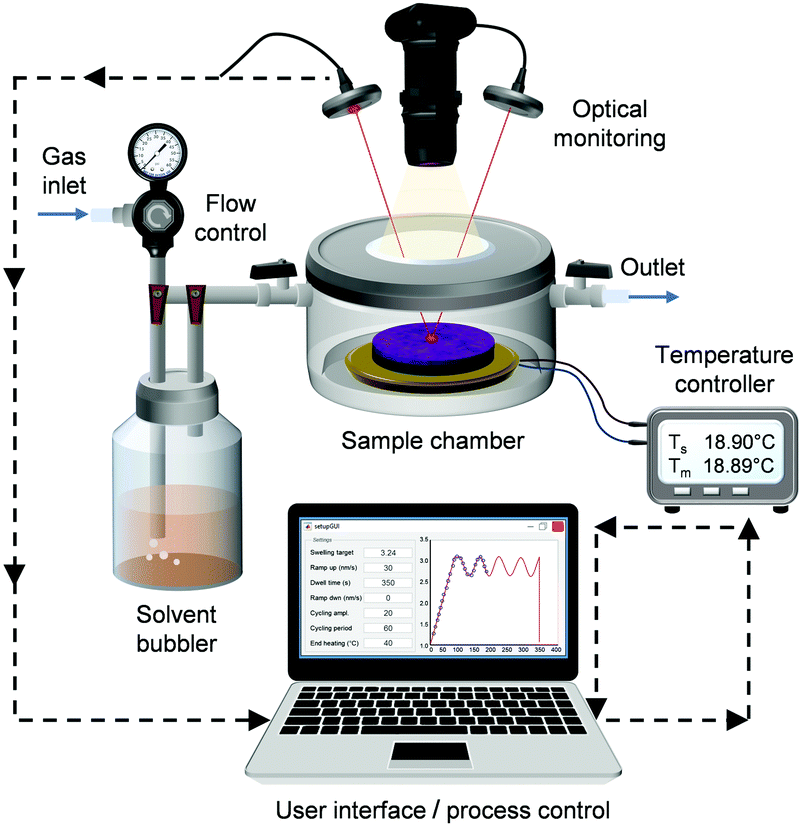 | ||
| Fig. 1 Schematic of the automated solvent vapor flow annealing system. | ||
The chamber lid is fully detachable and has a quartz window for optical monitoring. Spectroscopic reflectometry was used to monitor the swelling of the film via the change in film thickness. Spectral reflectance is measured every 30 ms over a 320–800 nm wavelength range. The thickness of the film is determined by continuously fitting the measured spectrum to a model of a single thin film on a substrate. The optical constants of a dry BCP thin film were assumed to follow the dispersion relation of the majority-component polymer. The thickness prior to SVA was also measured using an ellipsometer. In the case of dry PS–P2VP thin films (∼45 nm), the reflectometry and ellipsometry results differed from each other on average only by 1.1 nm proving that the chosen thin film model is valid. For swollen films, the spectral reflectance fitting worked best when the thin film was assumed to have a refractive index that changed with the addition of solvent. A video of the real-time thickness fitting during SVA can be found in the ESI† (Video SV1).
A CMOS camera with a long working distance objective operating in dark-field illumination provides live video of the thin film during annealing. The video feed can be used to monitor the quality of the films and quantify film dewetting. The largest area that can be viewed is ∼1 cm × 1 cm. Thus, in case of small wafer pieces, the whole sample surface could be monitored. Similar video monitoring of film dewetting has been implemented by Jin et al.44 with a more limited field of view. Other possible in situ characterization methods include epifluorescence microscopy, quartz crystal microbalances42 and GISAXS.30,36,37
Control of film swelling
According to our understanding, the swelling of the thin films in our system is controlled by changing the relative saturation of the solvent vapor using temperature. It has been shown that higher relative saturation increases the swelling of polymer films.41,48,49 The extent of the swelling depends on the solubility of the polymer in the solvent.50 In our SVA system, the relative saturation can be increased in the vicinity of the sample by decreasing the stage temperature, which pushes more solvent into the BCP film. An increase in the temperature has the opposite effect. This type of swelling control mechanism is very fast and remarkably precise if the feedback loop and temperature response of the sample stage are fast enough.The relative saturation P/Peq is the ratio of the partial pressure of the solvent in the chamber to the equilibrium vapor pressure. As displayed in Fig. 2a, both pressures can be altered by changing the temperature. The equilibrium vapor pressure of a solvent is given by the semi-empirical Antoine equation:
| Peq [mmHg] = 10A−B/(C+T) | (1) |
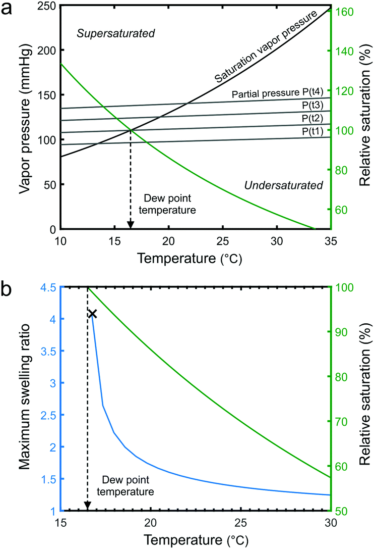 | ||
| Fig. 2 (a) Temperature dependence of the saturation vapor pressure and the partial pressure of THF in the chamber. The four different P(t1)–P(t4) scenarios represent increasing filling of the chamber with THF vapor. The relative saturation P(t2)/Peq changes with the temperature. (b) The maximum calculated sorption of THF into a PS thin film increases with increasing relative saturation. Vapor begins to condense close to the dew point temperature (P(t2)/Peq = 100%) and the polymer dewets. | ||
The swelling behavior of polymer thin films can be modelled as a dissolution process according to regular solution theory. At a relative saturation P/Peq, the maximum equilibrium sorption of solvent into a homopolymer thin film can be described as:50
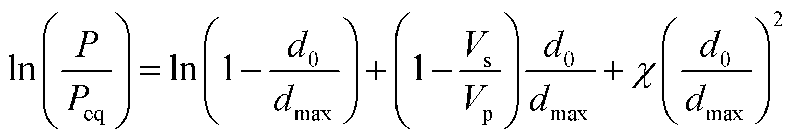 | (2) |
The maximum equilibrium sorption of THF into a PS thin film is modelled in Fig. 2b. It can be observed that the swelling ratio becomes highly sensitive to the relative vapor saturation as the dew point temperature is approached. Close to the dew point, minute changes in the temperature (T < ±0.5 °C) are enough to drastically modulate the swelling ratio. Our SVA device with its temperature-controlled stage can operate in this region, a few tenths of a degree from the dew point, without issues with solvent condensation. The tuning of the P/Peq is effective primarily in the vicinity of the sample and stage surface (ESI,† Fig. S1 shows a measurement for water vapor). Since the solvent vapor is not close to the dew point elsewhere in the chamber, the chamber walls, lid and gas pipes do not need to be heated to prevent unwanted condensation. However, should the stage temperature decrease below the dew point, solvent vapor will condense on the stage and thin film swelling will become uncontrollable.
Automated annealing
One of our aims was to improve the reliability of SVA, which is essential for an industrially viable lithography technique. Therefore, a MATLAB based script was written to handle the annealing process from data collection to signal processing, computation and instrument control. The Instrument Controller Toolbox of MATLAB was set to communicate with the spectrometer, TEC module and the CMOS camera. A user-friendly graphical interface was built on top where the user could design the annealing run and set the relevant parameters. During the annealing run the thickness of the BCP thin film follows a predetermined swelling profile. The swelling of the thin film is actively controlled via the temperature of the sample stage. The thickness of the swollen film is compared to the target set point and the temperature is adjusted accordingly via a PID (proportional-integral-derivative) control feedback mechanism. The feedback loop is capable of controlling the film swelling every 30 ms. Mean deviation from the thickness target set point is typically smaller than ±0.2 nm. The swelling ratio SR is calculated as the thickness of the swollen film d divided by the original film thickness d0.Fig. 3 displays the optically measured swelling of a high-molecular weight PS–P2VP thin film during feedback-controlled and uncontrolled SVA in THF, toluene and acetone. The uncontrolled SVA was performed by keeping the stage at a constant temperature (T = 20 °C) and using a constant vapor flow. The shape of the swelling curve is greatly affected by the set flow rate and the solubility of the BCP in the solvent. According to Hildebrand53 solubility parameters, toluene (δTOL = 18.2 MPa1/2) is considered a good solvent for the PS-majority PS–P2VP (δPS = 18.7 MPa1/2) and thus the BCP swells more in toluene than in a less-suitable solvent such as acetone (δACE = 20.3 MPa1/2). Overall, the solvent uptake in uncontrolled SVA is quite slow and the maximum swelling ratio is relatively low. Room temperature fluctuations and seasonal changes are also known to influence the swelling curve when no feedback loop is implemented.44 The feedback-controlled thin film swelling presented in Fig. 3 and Fig. S2, S3 (ESI†) follows a predetermined swelling profile. The profile consists of an unrestricted solvent uptake period (10–40 s), a linear up-ramping regime at a predetermined rate, a steady dwell regime and a deswelling or quenching regime. The deswelling of the thin film can be done at a controlled rate (nm min−1). Solvent can also be removed instantly (quenching) to preserve the morphology obtained in the swollen state by purging the chamber with N2. The removal of the residual solvent content can be enhanced by simultaneously heating up the sample stage to 40–50 °C. In this type of feedback-controlled SVA device, BCP thin films can be made to swell quickly and to the desired swelling ratio, irrespective of the type of solvent used. The swelling control method based on relative saturation is applicable to not only different solvents but also different polymers. The controlled swelling of PDMS-majority PS–PDMS is demonstrated in ESI,† Fig. S3. Similar to the PS–P2VP, the uncontrolled film swelling of PS–PDMS in toluene is moderate but with the feedback-control, high SR can be reached. The temperature-controlled feedback system also eliminates the unwanted swelling variations that would arise from seasonal changes or changes in the ambient temperature.
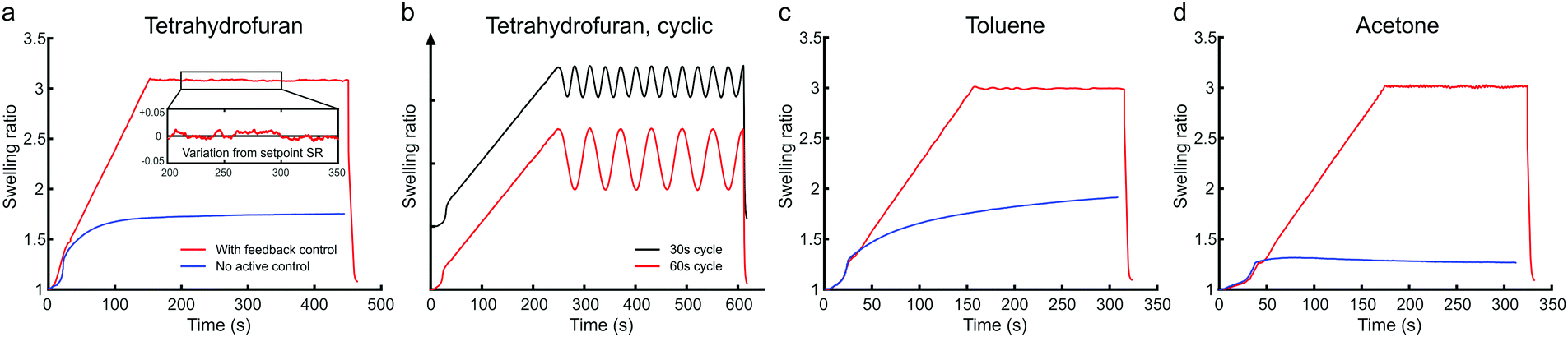 | ||
| Fig. 3 Solvent annealing profiles of high-molecular weight PS–P2VP thin films annealed in (a) and (b) THF, (c) toluene and (d) acetone. The uncontrolled swelling of the BCP film in each solvent is displayed in blue while feedback-controlled swelling according to a predetermined high-SR swelling profile is in red or black. Inset in (a) displays the deviation of the measured SR from the set point. The possibility of cyclic annealing is shown in (b) with cyclic modulation of the SR in 30 s and 60 s periods. The cyclic profiles are vertically offset for clarity. | ||
The fast, controlled modulation of the film swelling enables the use of complex annealing profiles. In our SVA device, the steady dwell regime can be replaced with controlled ramping or cycling regimes. Fig. 3(b) demonstrates two annealing profiles, where the film swelling ratio was modulated rapidly in 30 s and 60 s cycles. The cycle period can be as fast as 5 s in feedback-controlled operation and less than 1 s in an open-loop system that does not use the measured SR as a corrective input. Dynamical simulations have suggested that repeating swelling and deswelling cycles could improve the perpendicular orientation of BCP domains in thick BCP films.54 To the best of our knowledge, this is the first time that fast cyclic solvent annealing has been experimentally realized.
Performance evaluation with high-molecular weight BCPs
The SVA process has notably been susceptible to even minor changes in the annealing conditions or the surrounding environment making reproducibility an issue. Predetermined swelling profiles make it possible to precisely repeat experiments and explore how different process parameters influence the self-organization behavior of BCPs. The degree of swelling, SR, has been recognized via GISAXS studies to dictate order–order and order–disorder transitions in the BCP films, and influence the domain spacing and the degree of lateral ordering.30,37 To verify the functionality of our annealing device we scrutinized the effect of the SR on the morphology of high-MW PS–P2VP thin films.In the first experiment 45 nm thick PS–P2VP (Mn = 188 kg mol−1) films were spin-coated on unmodified Si wafers from toluene–THF solutions. Fig. 4 displays scanning electron microscope (SEM) images of the platinum-stained BCP thin films after annealing with increasing swelling ratios using THF as a near-neutral annealing solvent. A ramp up rate of 0.6 SR per min was used and quenching was done immediately when target was reached with no dwell period. The micellar-like as-spun morphology was observed to improve with increasing swelling ratio until SR ∼ 3.5. A well-ordered hexagonally packed cylinder morphology with a domain spacing L0 ∼ 75 nm could be achieved in 4 minutes – or in little over 2 minutes if the ramp rate was increased to 1.0 SR per min.
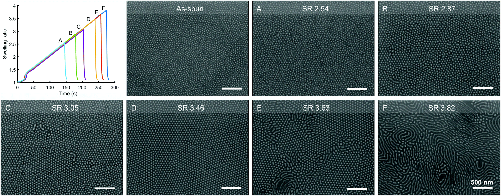 | ||
| Fig. 4 Cylinder-forming PS–P2VP 188 kg mol−1 thin films annealed in THF at increasing swelling ratios. Films were quenched when target SR was reached to preserve the obtained BCP morphology. SEM images (A)–(F) of the platinum stained thin films display the change in BCP morphology with increasing SR values. Perpendicularly oriented and well-ordered cylinders were achieved around SR = 3.5 (D). Terracing occurred with SR > 3.6 (E and F). | ||
With SR > 3.6 the 188 kg mol−1 thin films exhibited a mixed morphology consisting of regions with perpendicular and parallel cylinders. The regions appeared to be single- and multi-layer areas that followed spinodal decomposition patterns. The appearance of these areas as well as possible dewetting could be observed during annealing from the camera images. Multilayering or terracing is known to occur due to commensurability issues between the film thickness and the equilibrium domain spacing L0 of the BCP morphology.55,56 Here terracing occurred when SR × d0 > 2L0. With higher SR, the film morphology consisted mainly of parallel cylinders that grew in length but with no significant lateral order. This morphology behavior is consistent with previous research on the effects of SR on low-molecular weight polystyrene–polylactide BCPs (18–75 kg mol−1).47
The self-assembly of high-MW BCPs is typically hindered by the low mobility of long-chained polymers. As a result, it is challenging to achieve good lateral ordering of the BCP features, and solvent annealing of high-MW BCPs can take hours6,15 or even days.57 We tried annealing 258 kg mol−1 PS–P2VP thin films at a maximum feasible SR and then examined the growth of ordered cylinder grains in time. Fig. 5 and Fig. S4a (ESI†) illustrate the defect density of 258 kg mol−1 PS–P2VP thin films after 0 min, 10 min and 25 min of annealing dwell time. The blue regions depict locations where the lattice is not perfectly hexagonal, i.e. the PVP cylinders have fewer or more than six neighboring cylinders. The lattice defect density after up-ramping was 31.2 defects per μm2, which deceased to 17.4 μm−2 after 10 min and finally to 15.6 μm−2 after 25 min of dwell time. This shows that grain coarsening and point defect annihilation is fastest during the first 10 minutes, after which the grain growth slows down. This is consistent with the grain size coarsening following a power-law ξ ∼ tα where α = 0.2–0.3 for thin films.26,58 After 25 min of dwell time there are very few point defects left and most of the lattice imperfections arise from the grain boundaries. Elimination of these grain boundary defects would require significant reorientation of neighboring grains.
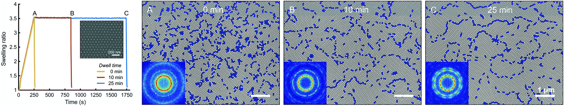 | ||
| Fig. 5 Cylinder-forming PS–P2VP 258 kg mol−1 thin films annealed in THF at same swelling ratio but with increasing dwell times. (A)–(C) Defects in the BCP morphology after 0, 10 and 25 min of annealing dwell time. Perfectly ordered regions are mapped in gray. Defect locations where the hexagonal lattice is not six-fold coordinated are mapped in blue. Insets (A)–(C) show FFT of SEM images. | ||
Previous research has shown that the highest degree of order and the largest grain sizes are achieved when solvent annealing is done close to the ODT limit.36,38 Our swelling studies using high segregation strength BCPs were restricted more by the film commensurability than the ODT. SVA was done at an SR value that was just below the multilayering limit. A cautious estimate of the ODT concentration of 258 kg mol−1 PS–P2VP (N ∼ 2480) would be ϕPS–P2VP = 0.136, corresponding to a SR of 7.33 (see ESI† for calculation). Thus, higher SR values could likely be used and larger grains achieved if the cylinder reorientation process was suppressed. This could be done using neutral brush layers or top coats that govern the preferred orientation of the BCP domains.59–61 On unmodified substrates, the largest grain sizes that we achieved with the high-MW BCPs were in the range of several microns. Long-distance order and alignment can be achieved using substrates with topographic or chemical patterns that direct the self-assembly of the BCPs (DSA). We also tested the feedback-controlled SVA with these types of prepatterned substrates. The DSA of high-MW PS–P2VP on a Si trench pattern is demonstrated in Fig. S4b (ESI†), where highly aligned rows of perpendicular cylinders were achieved along the trench length.
The possibility of large area self-assembly was also explored since BCP lithography would be ideal for engineering materials with new surface properties. Subwavelength BCP patterns have been already used to produce nanostructured antireflective coatings17 and anisotropic refractive index metamaterials.19 So far, we have managed to optimize the whole BCP self-assembly and SVA process for quarter pieces of 2-inch Si wafers. Perpendicularly oriented BCP cylinders with a large grain size could be achieved over the quarter wafer by combining a high SR value (3.0 < SR< 3.5) with a 10–15 min annealing dwell time. Fig. 6a shows an unpatterned Si quarter wafer and a wafer where the 188 kg mol−1 PS–P2VP cylinder pattern has been etched into the Si surface. The shallow pores depicted in Fig. 6b modify the refractive index of the Si surface,62 which can be seen as a uniform color change over the patterned area. A full analysis of the BCP morphology over a quarter wafer can be found in ESI,† Fig. S5.
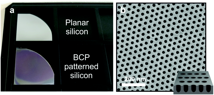 | ||
| Fig. 6 (a) High-MW BCP self-assembly done on quarter-wafer scale using the automated SVA system. The BCP cylinder pattern is etched into Si causing the wafer color to change due to an effective refractive index change. (b) Top-down SEM image of the dry etched Si surface. The inset depicts the shallow pore structure that is obtained. | ||
Conclusions
Improvements in scalability and reliability are a key step in making BCP lithography commercially viable. Also better control, understanding and reproducibility of the solvent annealing process are needed. Since the solvent content in the thin films is an essential factor governing the final morphology and lateral order, more precise control of the swelling is required. In this paper, we describe the design and operation of an automated SVA system that is capable of modulating the film swelling with nanometer precision. The film swelling behavior is manipulated by changing the relative vapor saturation locally, near the surface of the sample. This control implementation uses local heating or cooling, which is a much faster method than the typical one using gas flow mixing. The advantage of feedback-controlled swelling is that the annealing process becomes insensitive to minor variations in the ambient conditions, gas flow rate and solvent vapor concentration.With feedback-controlled SVA, different aspects of the film swelling profile can be isolated and their influence on the BCP self-assembly evaluated. For practical applications, the influence of SVA parameters on defect reduction, lateral ordering and self-assembly kinetics are of great interest. We demonstrated the utility of the SVA device by annealing high segregation strength polymers that typically display slow self-assembly kinetics due to low chain mobility. We have shown that 258 kg mol−1 PS–P2VP thin films can be made to self-organize into well-ordered cylinder patterns in under 15 minutes by optimizing the swelling profile. Complex swelling profiles are also possible, and we demonstrated controlled cyclic solvent annealing for the first time.
Experimental section
Thin film preparation
PS–P2VP cylinder-forming diblock copolymers were purchased from Polymer Source Inc. and used as received. The number average molecular weights of the BCPs were 258 kg mol−1 (MPS = 185 kg mol−1, MPVP = 73 kg mol−1, PDI = 1.17) and 188 kg mol−1 (MPS = 135 kg mol−1, MPVP = 53 kg mol−1, PDI = 1.18) with a PS volume fraction fPS = 0.72. Analytical grade solvents acetone, toluene and anhydrous tetrahydrofuran (THF, contains 250 ppm BHT as inhibitor) were obtained from Sigma-Aldrich. The BCPs were dissolved in a 7![[thin space (1/6-em)]](https://www.rsc.org/images/entities/char_2009.gif) :3 mixture of toluene:THF to obtain 0.5–1.0% (w/v) solutions. The solutions were left to stir overnight and filtered using a 0.22 μm pore size syringe filter to remove any undissolved particulates. Test grade (100) silicon wafers with the native oxide intact were washed using acetone and isopropanol followed by oxygen plasma cleaning for 1 min (Oxford Plasmalab System100). The BCP thin films were fabricated on 1/4 pieces of 2-inch Si wafers by spin coating at 2500–3000 rpm for ∼60 s in a closed chamber SSE OPTIcoat spinner. The thin films were immediately soft-baked at 125 °C for 2 min to remove any residual solvent. Samples were diced into 1 cm × 1 cm pieces and the initial thickness of the films was measured from the center of the pieces using a HeNe laser ellipsometer (Rudolph Research AutoEL III) at a 70° incident angle.
:3 mixture of toluene:THF to obtain 0.5–1.0% (w/v) solutions. The solutions were left to stir overnight and filtered using a 0.22 μm pore size syringe filter to remove any undissolved particulates. Test grade (100) silicon wafers with the native oxide intact were washed using acetone and isopropanol followed by oxygen plasma cleaning for 1 min (Oxford Plasmalab System100). The BCP thin films were fabricated on 1/4 pieces of 2-inch Si wafers by spin coating at 2500–3000 rpm for ∼60 s in a closed chamber SSE OPTIcoat spinner. The thin films were immediately soft-baked at 125 °C for 2 min to remove any residual solvent. Samples were diced into 1 cm × 1 cm pieces and the initial thickness of the films was measured from the center of the pieces using a HeNe laser ellipsometer (Rudolph Research AutoEL III) at a 70° incident angle.
Solvent annealing device setup
The SVA chamber consisted of a custom-made stainless steel body and a detachable lid. The chamber had a maximum internal volume of V = 103 ml and could fit substrate wafers up to 2 inch in diameter. The copper stage plate was bonded to a thermoelectric cooler module (MultiComp, TEC 110 W, 12 A). The TEC element could either heat or cool the stage depending on the direction and magnitude of an electrical current driven through it (Thorlabs ITC4005 TEC controller). Temperature of the sample stage was monitored with a temperature transducer (AD590MF) for the feedback loop.Dry nitrogen gas was bubbled through a temperature-stabilized solvent reservoir to generate the solvent vapor. The flow rate of the carrier gas was set constant using a gas regulator and a Brooks Instrument Sho-rate gas flow meter. The solvent vapor was fed into the chamber from a ring-structure at the bottom to ensure more uniform vapor distribution. The chamber inlet and outlet were equipped with ball valves making it possible to cut off all flows and make the chamber airtight. The solvent reservoir could also be bypassed so that pure nitrogen gas was fed through the chamber (purging). A Thorlabs TSP01 USB Data Logger was installed inside the SVA chamber to monitor the temperature of the gas vapor. The whole SVA setup was constructed in a temperature and humidity controlled clean room to minimize external influences.
The chamber allowed optical monitoring through a quartz viewport. A USB-connected CMOS camera (Thorlabs DCC1645C) was installed above the viewport to provide live video of the thin film surface during annealing. An LED ring light (Thorlabs OSL2 Fiber Illuminator) was used for sample illumination and the system was set up to record in dark-field mode. The thickness and swelling of the polymer film was determined in situ using spectroscopic reflectometry with an Ocean Optics spectrometer (HR4000) and a UV-Vis light source with a spot size of approx. 4 mm. To account for changes in the signal intensity and ambient lighting, the system was calibrated and referenced using a clean Si wafer before each run. The dry and swollen film thicknesses were determined by fitting a thin film model to the measured spectral data in real-time.63 The model used optical constants that change with the addition of solvent according to the Lorentz–Lorenz rule of mixing.64 For PS–P2VP, it was assumed the refractive index would comply with that of the majority block PS. Either a constant refractive index (nPS = 1.59) or a wavelength dependent dispersion formula65 was applicable. A refractive index of 1.407 was used for THF. Dispersion equations were used for toluene66 and acetone.67
Automated annealing process
The BCP thin films were annealed in the solvent annealing device described above. The system was operated via a graphical user interface that was connected to the TEC controller, spectrometer and CMOS camera. Samples were placed on the TEC plate in the chamber and the chamber was flushed with dry N2. Solvent vapor was introduced into the chamber via the temperature-stabilized bubbler at a constant N2 carrier flow rate of 100 ml min−1. BCP films were annealed in the solvent + N2 vapor flow so that the film SR (or thickness) followed a predetermined profile. The extent of swelling was measured in real-time using reflectometry and controlled using a feedback loop that automatically adjusted the temperature of the sample stage by TEC. Currently, only the proportional gain in the PID controller was used. The up ramping rates were varied from 0.6 to 1.0 SR per min and annealing (dwell) times from 0 to 25 min. At the end, the swollen thin films were vitrified by purging the chamber with dry N2. Additional heating (40 °C) was used to remove the residual solvent from the films.Sample characterization
A metal salt infiltration process68 was used to enhance imaging contrast between the two blocks of the BCP. The thin films were immersed in a 1 mM Na2PtCl4 + 0.1% HCl(aq) solution for 10–15 min, washed with deionized water and blow dried with nitrogen. The anionic platinum complexes bind specifically to the protonated PVP domains. The morphologies of the platinum-stained BCP films were examined with a field-emission scanning electron microscope (Carl Zeiss ULTRA 55) operated at 3 kV. For BCP lithography, the PVP cylinders were selectively removed by dipping in warm ethanol and the pattern was etched into Si by SF6/O2 dry etching.62Morphology analysis and defect counting were done using ImageJ269 and MATLAB R2015b. The SEM images were converted into binary black-and-white images with automatic thresholding and noise was reduced by removing outlier pixels. The center positions were used to generate a Voronoi diagram, and the number of vertex edges was counted to determine the amount of lattice defects. The periodic hexagonal morphology was analyzed using Fast Fourier Transform (FFT) from 1024 × 1024 pixel binary images.
Conflicts of interest
There are no conflicts to declare.Acknowledgements
We would like to thank Markus Hiekkamäki for programming the interface between the external hardware and the control software for our solvent annealing device. We thank also Dr Sokol Ndoni from the Technical University of Denmark for providing the PS-PDMS polymers. This work was supported by Tampere University under Grant No. #83026. The work is part of the Academy of Finland Flagship Programme, Photonics Research and Innovation (PREIN), decision #320165.Notes and references
- C. M. Bates and F. S. Bates, Macromolecules, 2017, 50, 3–22 CrossRef CAS.
- C. Park, J. Yoon and E. L. Thomas, Polymer, 2003, 44, 6725–6760 CrossRef CAS.
- M. A. Chavis, D.-M. Smilgies, U. B. Wiesner and C. K. Ober, Adv. Funct. Mater., 2015, 25, 3057–3065 CrossRef CAS PubMed.
- A. Rahman, P. W. Majewski, G. Doerk, C. T. Black and K. G. Yager, Nat. Commun., 2016, 7, 13988 CrossRef PubMed.
- J. G. Kennemur, L. Yao, F. S. Bates and M. A. Hillmyer, Macromolecules, 2014, 47, 1411–1418 CrossRef CAS.
- E. Kim, H. Ahn, S. Park, H. Lee, M. Lee, S. Lee, T. Kim, E.-A. Kwak, J. H. Lee, X. Lei, J. Huh, J. Bang, B. Lee and D. Y. Ryu, ACS Nano, 2013, 7, 1952–1960 CrossRef CAS PubMed.
- Q. P. Chen, L. Barreda, L. E. Oquendo, M. A. Hillmyer, T. P. Lodge and J. I. Siepmann, ACS Nano, 2018, 12, 4351–4361 CrossRef CAS.
- J. K. D. Mapas, T. Thomay, A. N. Cartwright, J. Ilavsky and J. Rzayev, Macromolecules, 2016, 49, 3733–3738 CrossRef CAS.
- R. N. Carmean, T. E. Becker, M. B. Sims and B. S. Sumerlin, Chem, 2017, 2, 93–101 CAS.
- J. Frascaroli, S. Brivio, F. Ferrarese Lupi, G. Seguini, L. Boarino, M. Perego and S. Spiga, ACS Nano, 2015, 9, 2518–2529 CrossRef CAS.
- A. Kikitsu, T. Maeda, H. Hieda, R. Yamamoto, N. Kihara and Y. Kamata, IEEE Trans. Magn., 2013, 49, 693–698 CAS.
- M. P. Stoykovich, H. Kang, K. C. Daoulas, G. Liu, C.-C. Liu, J. J. de Pablo, M. Müller and P. F. Nealey, ACS Nano, 2007, 1, 168–175 CrossRef CAS PubMed.
- H. Yi, X. Y. Bao, R. Tiberio and H. S. P. Wong, Nano Lett., 2015, 15, 805–812 CrossRef CAS PubMed.
- C.-C. Liu, E. Franke, Y. Mignot, R. Xie, C. W. Yeung, J. Zhang, C. Chi, C. Zhang, R. Farrell, K. Lai, H. Tsai, N. Felix and D. Corliss, Nat. Electron., 2018, 1, 562–569 CrossRef CAS.
- S. Park, Y. Kim, H. Ahn, J. H. Kim, P. J. Yoo and D. Y. Ryu, Sci. Rep., 2016, 6, 36326 CrossRef.
- S. Rasappa, H. Hulkkonen, L. Schulte, S. Ndoni, J. Reuna, T. Salminen and T. Niemi, J. Colloid Interface Sci., 2019, 534, 420–429 CrossRef CAS PubMed.
- P. Mokarian-Tabari, R. Senthamaraikannan, C. Glynn, T. W. Collins, C. Cummins, D. Nugent, C. O’Dwyer and M. A. Morris, Nano Lett., 2017, 17, 2973–2978 CrossRef CAS.
- S. Vignolini, N. A. Yufa, P. S. Cunha, S. Guldin, I. Rushkin, M. Stefik, K. Hur, U. Wiesner, J. J. Baumberg and U. Steiner, Adv. Mater., 2012, 24, OP23–OP27 CrossRef CAS PubMed.
- J. Y. Kim, H. Kim, B. H. Kim, T. Chang, J. Lim, H. M. Jin, J. H. Mun, Y. J. Choi, K. Chung, J. Shin, S. Fan and S. O. Kim, Nat. Commun., 2016, 7, 12911 CrossRef.
- IEEE, International Roadmap for Devices and Systems 2017 – Emerging Research Materials, https://irds.ieee.org/editions/2017.
- L. D. Williamson, R. N. Seidel, X. Chen, H. S. Suh, P. Rincon Delgadillo, R. Gronheid and P. F. Nealey, ACS Appl. Mater. Interfaces, 2016, 8, 2704–2712 CrossRef CAS PubMed.
- T.-H. Chang, S. Xiong, R. M. Jacobberger, S. Mikael, H. S. Suh, C.-C. Liu, D. Geng, X. Wang, M. S. Arnold, Z. Ma and P. F. Nealey, Sci. Rep., 2016, 6, 31407 CrossRef PubMed.
- I. Bita, J. K. W. Yang, Y. S. Jung, C. A. Ross, E. L. Thomas and K. K. Berggren, Science, 2008, 321, 939–943 CrossRef CAS PubMed.
- S.-J. Jeong, J. E. Kim, H.-S. Moon, B. H. Kim, S. M. Kim, J. B. Kim and S. O. Kim, Nano Lett., 2009, 9, 2300–2305 CrossRef CAS.
- F. Ferrarese Lupi, T. J. Giammaria, M. Ceresoli, G. Seguini, K. Sparnacci, D. Antonioli, V. Gianotti, M. Laus and M. Perego, Nanotechnology, 2013, 24, 315601 CrossRef CAS.
- P. W. Majewski and K. G. Yager, Soft Matter, 2016, 12, 281–294 RSC.
- C. Sinturel, M. Vayer, M. Morris and M. A. Hillmyer, Macromolecules, 2013, 46, 5399–5415 CrossRef CAS.
- S. H. Kim, M. J. Misner, T. Xu, M. Kimura and T. P. Russell, Adv. Mater., 2004, 16, 226–231 CrossRef CAS.
- Y. S. Jung and C. A. Ross, Nano Lett., 2007, 7, 2046–2050 CrossRef CAS.
- M. Y. Paik, J. K. Bosworth, D.-M. Smilgies, E. L. Schwartz, X. Andre and C. K. Ober, Macromolecules, 2010, 43, 4253–4260 CrossRef CAS PubMed.
- S. Rasappa, L. Schulte, D. Borah, H. Hulkkonen, S. Ndoni, T. Salminen, R. Senthamaraikannan, M. A. Morris and T. Niemi, Microelectron. Eng., 2018, 192, 1–7 CrossRef CAS.
- X. Zhang, K. D. Harris, N. L. Y. Wu, J. N. Murphy and J. M. Buriak, ACS Nano, 2010, 4, 7021–7029 CrossRef CAS PubMed.
- W. I. Park, K. Kim, H. I. Jang, J. W. Jeong, J. M. Kim, J. Choi, J. H. Park and Y. S. Jung, Small, 2012, 8, 3762–3768 CrossRef CAS.
- W. I. Park, S. Tong, Y. Liu, I. W. Jung, A. Roelofs and S. Hong, Nanoscale, 2014, 6, 15216–15221 RSC.
- W. I. Park, Y. J. Choi, J. M. Yun, S. W. Hong, Y. S. Jung and K. H. Kim, ACS Appl. Mater. Interfaces, 2015, 7, 25843–25850 CrossRef CAS PubMed.
- X. Gu, I. Gunkel, A. Hexemer and T. P. Russell, Macromolecules, 2016, 49, 3373–3381 CrossRef CAS.
- X. Gu, I. Gunkel, A. Hexemer, W. Gu and T. P. Russell, Adv. Mater., 2014, 26, 273–281 CrossRef CAS.
- A. Baruth, M. Seo, C. H. Lin, K. Walster, A. Shankar, M. A. Hillmyer and C. Leighton, ACS Appl. Mater. Interfaces, 2014, 6, 13770–13781 CrossRef CAS PubMed.
- K. A. Cavicchi and T. P. Russell, Macromolecules, 2007, 40, 1181–1186 CrossRef CAS.
- J. D. Cushen, L. Wan, G. Pandav, I. Mitra, G. E. Stein, V. Ganesan, R. Ruiz, C. G. Willson and C. J. Ellison, J. Polym. Sci., Part B: Polym. Phys., 2014, 52, 36–45 CrossRef CAS.
- K. W. Gotrik, A. F. Hannon, J. G. Son, B. Keller, A. Alexander-Katz and C. A. Ross, ACS Nano, 2012, 6, 8052–8059 CrossRef CAS PubMed.
- D. T. Hoang, J. Yang, K. Paeng, Y. Kwon, O. S. Kweon and L. J. Kaufman, Rev. Sci. Instrum., 2016, 87, 015106 CrossRef PubMed.
- D. Posselt, J. Zhang, D.-M. Smilgies, A. V. Berezkin, I. I. Potemkin and C. M. Papadakis, Prog. Polym. Sci., 2017, 66, 80–115 CrossRef CAS.
- C. Jin, B. C. Olsen, E. J. Luber and J. M. Buriak, Chem. Mater., 2017, 29, 176–188 CrossRef CAS.
- R. Lundy, S. P. Flynn, C. Cummins, S. M. Kelleher, M. N. Collins, E. Dalton, S. Daniels, M. A. Morris and R. Enright, Phys. Chem. Chem. Phys., 2017, 19, 2805–2815 RSC.
- G. Nelson, C. Drapes, M. Grant, R. Gnabasik, J. Wong and A. Baruth, Micromachines, 2018, 9, 271 CrossRef PubMed.
- A. Baruth, M. Seo, C. H. Lin, K. Walster, A. Shankar, M. A. Hillmyer and C. Leighton, ACS Appl. Mater. Interfaces, 2014, 6, 13770–13781 CrossRef CAS PubMed.
- A. Knoll, R. Magerle and G. Krausch, J. Chem. Phys., 2004, 120, 1105–1116 CrossRef CAS PubMed.
- B.-J. Niebuur, J. Puchmayr, C. Herold, L. Kreuzer, V. Hildebrand, P. Müller-Buschbaum, A. Laschewsky and C. Papadakis, Materials, 2018, 11, 850 CrossRef PubMed.
- J. Jaczewska, A. Budkowski, A. Bernasik, I. Raptis, J. Raczkowska, D. Goustouridis, J. Rysz and M. Sanopoulou, J. Appl. Polym. Sci., 2007, 105, 67–79 CrossRef CAS.
- I. Smallwood, Handbook of Organic Solvent Properties, Elsevier, Oxford, 1996 Search PubMed.
- J. A. Emerson, D. T. W. Toolan, J. R. Howse, E. M. Furst and T. H. Epps, Macromolecules, 2013, 46, 6533–6540 CrossRef CAS.
- W. Zeng, Y. Du, Y. Xue and H. L. Frisch, in Physical Properties of Polymers Handbook, ed. J. E. Mark, Springer New York, New York, 2007, pp. 289–303 Search PubMed.
- S. P. Paradiso, K. T. Delaney, C. J. García-Cervera, H. D. Ceniceros and G. H. Fredrickson, Macromolecules, 2016, 49, 1743–1751 CrossRef CAS.
- C. T. Black, C. Forrey and K. G. Yager, Soft Matter, 2017, 13, 3275–3283 RSC.
- M. J. Maher, J. L. Self, P. Stasiak, G. Blachut, C. J. Ellison, M. W. Matsen, C. M. Bates and C. G. Willson, ACS Nano, 2016, 10, 10152–10160 CrossRef CAS PubMed.
- Q. Yang and K. Loos, Polymers, 2017, 9, 525 CrossRef PubMed.
- C. T. Black and K. W. Guarini, J. Polym. Sci., Part A: Polym. Chem., 2004, 42, 1970–1975 CrossRef CAS.
- H. Yoshida, H. S. Suh, A. Ramírez-Hernández, J. I. Lee, K. Aida, L. Wan, Y. Ishida, Y. Tada, R. Ruiz, J. de Pablo and P. F. Nealey, J. Photopolym. Sci. Technol., 2013, 26, 55–58 CrossRef CAS.
- W. J. Durand, M. C. Carlson, M. J. Maher, G. Blachut, L. J. Santos, S. Tein, V. Ganesan, C. J. Ellison and C. G. Willson, Macromolecules, 2016, 49, 308–316 CrossRef CAS.
- S. Ji, C.-C. Liu, J. G. Son, K. Gotrik, G. S. W. Craig, P. Gopalan, F. J. Himpsel, K. Char and P. F. Nealey, Macromolecules, 2008, 41, 9098–9103 CrossRef CAS.
- H. H. Hulkkonen, T. Salminen and T. Niemi, ACS Appl. Mater. Interfaces, 2017, 9, 31260–31265 CrossRef CAS PubMed.
- P. Yeh, Optical waves in layered media, Wiley-Interscience, Hoboken, NJ, 2005 Search PubMed.
- R. Mehra, J. Chem. Sci., 2003, 115, 147–154 CrossRef CAS.
- N. Sultanova, S. Kasarova and I. Nikolov, Acta Phys. Pol., A, 2009, 116, 585–587 CrossRef CAS.
- S. Kedenburg, M. Vieweg, T. Gissibl and H. Giessen, Opt. Mater. Express, 2012, 2, 1588 CrossRef CAS.
- J. Rheims, J. Köser and T. Wriedt, Meas. Sci. Technol., 1997, 8, 601–605 CrossRef CAS.
- J. Chai, D. Wang, X. Fan and J. M. Buriak, Nat. Nanotechnol., 2007, 2, 500–506 CrossRef PubMed.
- C. T. Rueden, J. Schindelin, M. C. Hiner, B. E. DeZonia, A. E. Walter, E. T. Arena and K. W. Eliceiri, BMC Bioinf., 2017, 18, 529 CrossRef PubMed.
Footnote |
| † Electronic supplementary information (ESI) available. See DOI: 10.1039/c9sm01322a |
| This journal is © The Royal Society of Chemistry 2019 |