
 Open Access Article
 This Open Access Article is licensed under a
 Creative Commons Attribution 3.0 Unported Licence
Nanocomposite of nickel oxide nanoparticles and polyethylene oxide as printable hole transport layer for organic solar cells†
Marta
Ruscello
 a,
Tanmoy
Sarkar
b,
Artem
Levitsky
b,
Giovanni Maria
Matrone
c,
Nikolaos
Droseros
d,
Stefan
Schlisske
ae,
Eleni
Sachs
ae,
Patrick
Reiser
af,
Eric
Mankel
af,
Wolfgang
Kowalsky
ag,
Natalie
Banerji
d,
Natalie
Stingelin
ch,
Gitti L.
Frey
b and
Gerardo
Hernandez-Sosa
*ae
a,
Tanmoy
Sarkar
b,
Artem
Levitsky
b,
Giovanni Maria
Matrone
c,
Nikolaos
Droseros
d,
Stefan
Schlisske
ae,
Eleni
Sachs
ae,
Patrick
Reiser
af,
Eric
Mankel
af,
Wolfgang
Kowalsky
ag,
Natalie
Banerji
d,
Natalie
Stingelin
ch,
Gitti L.
Frey
b and
Gerardo
Hernandez-Sosa
*ae
aInnovationLab GmbH, Speyerer Strasse 4, 69115 Heidelberg, Germany
bDepartment of Materials Science and Engineering, Technion – Israel Institute of Technology, Haifa 32000, Israel
cDepartment of Materials and Centre for Plastic Electronics, Imperial College London, London SW7 2AZ, UK
dDepartment of Chemistry and Biochemistry, University of Bern, Freiestrasse 3, CH-3012 Bern, Switzerland
eLight Technology Institute, Karlsruhe Institute of Technology, Engesserstrasse 13, 76131 Karlsruhe, Germany. E-mail: gerardo.sosa@kit.edu
fSurface Science Division, Materials Science Department, Technische Universität Darmstadt, Jovanka-Bontschits-Straße 2, 64287 Darmstadt, Germany
gInstitut für Hochfrequenztechnik, Technische Universität Braunschweig, Schleinitzstrasse 22, 38106 Braunschweig, Germany
hSchool of Materials Science & Engineering, School of Chemical & Biomolecular Engineering, Georgia Institute of Technology, Ferst Drive, Atlanta, Georgia 30332, USA
First published on 8th April 2019
Abstract
We focused on the low-temperature fabrication (∼100 °C) of nanoparticle-based NiOx hole transport layers for organic solar cells. We used high molecular weight polyethylene oxide (PEO) as a sacrificial additive for the processing of NiOx nanoparticle (NP) dispersions which is removed from the film by oxygen plasma prior to the active layer deposition. Through comprehensive characterization by optical, electrical and scanning probe techniques we show that an optimal NiOx![[thin space (1/6-em)]](https://www.rsc.org/images/entities/char_2009.gif) :PEO ratio allows to disperse the NPs, hindering their aggregation and maximizing device performance. Finally, we demonstrate the practical relevance of our approach by inkjet printing the NiOx:PEO blends to produce hole transport layers (HTLs) for P3HT:PCBM bulk heterojunction solar cells with comparable efficiencies to devices produced with high-temperature precursor-based approaches. The utilization of P3HT:PCBM as active layer material is meant to offer an optimum standard for the introduction of the presented HTL processing approach and its applicability to a wider range of hybrid systems and multilayer optoelectronic devices.
:PEO ratio allows to disperse the NPs, hindering their aggregation and maximizing device performance. Finally, we demonstrate the practical relevance of our approach by inkjet printing the NiOx:PEO blends to produce hole transport layers (HTLs) for P3HT:PCBM bulk heterojunction solar cells with comparable efficiencies to devices produced with high-temperature precursor-based approaches. The utilization of P3HT:PCBM as active layer material is meant to offer an optimum standard for the introduction of the presented HTL processing approach and its applicability to a wider range of hybrid systems and multilayer optoelectronic devices.
Introduction
In the field of printable organic and hybrid electronics, increasing attention has been recently dedicated to novel interlayers that enable the optimal functioning of the electronic device.1–7 These interlayers provide an improved energetic alignment of the device electrodes to the semiconducting active layers, reducing contact resistance effects and providing a more efficient charge injection/extraction.8–13In recent years, high work-function solution-processed transition metal oxides (TMOs) such as non-stoichiometric nickel oxide (NiOx), molybdenum oxide (MoO3), vanadium oxide (V2O5), and tungsten oxide (WO3) have become promising candidates for hole injection/extraction interlayers for photovoltaic and organic light emitting devices.14 Particularly for photovoltaics, these TMOs have successfully been used to replace the commonly used PEDOT:PSS buffer layer due to their better chemical stability, lower acidity and hygroscopicity, as well as their high optical transparency and facile synthesis.4,6,15,16 NiOx is a p-type semiconductor and exhibits low electron affinity (1.8–2.1 eV), high work function (5.0–5.6 eV) and wide optical band gap (>3.0 eV). In contrast to MoO3, WO3, and V2O5, the valence band of NiOx is well aligned for hole transport with the highest occupied molecular orbital (HOMO) levels of many typical p-type conjugated polymers.17 Recently, NiOx layers, obtained through a sol–gel process from nickel organic salts precursors, have been successfully utilized in organic (OPV) and perovskite photovoltaic devices, showing improved device performance and stability.18–24 However, the used sol–gel process required a high temperature treatment (250–400 °C) to induce the decomposition of the precursor into a crystalline NiOx nanoparticle (NP) layer followed by a plasma treatment which further oxidizes the nanoparticles. The latter treatment enhances the non-stoichiometry of mixed nickel oxidation states, and, in-turn, the layer's conductivity.25,26 Such sol–gel systems can be printed using inkjet, leading to injection layers which display performances in various organic and dye-sensitized solar cells that are comparable to spin-coated systems.27–29 In spite of these encouraging results, the high processing temperatures that are required to produce well-performing layers are not compatible with flexible plastic substrates and would be a drawback for the fabrication of cost-efficient devices by high-throughput printing or coating technologies.30,31
In this work, we demonstrate a low temperature process (∼100 °C) for NiOx layers and their integration in organic solar cells by inkjet printing, via use of NiOx nanoparticles blended with high molecular weight polyethylene oxide (PEO) as a sacrificial processing additive that do not require any high temperature treatment.
Experimental section
NiOx layer fabrication
The NiOx dispersion (Avantama, Switzerland) was sonicated for 5 minutes before use and filtered with a 0.2 μm PTFE filter. PEO (Mw = 1000000 g mol−1, Sigma Aldrich) was dissolved in ethanol at a concentration of 1 mg ml−1 and kept at 50 °C in ambient atmosphere for at least 1 h before use. The PEO solution was then added to the NiOx dispersion to obtain blends NiOx:PEO with the content of NiOx ranging from 10 to 99.9% wt. These solutions were spin-coated in ambient condition with ω = 2000 rpm, a = 1000 rpm s−1 and t = 40 s just after mixing. The films were then annealed on a hot plate at 100 °C for 10 min and treated with oxygen plasma for 1 min. For inkjet-printed NiOx or NiOx:PEO layers, the NiOx:PEO compositions were kept the same as in the spin-coating process, though diethylene glycol was added to the ink formulation in a ratio of ethanol:diethylene glycol 1:3 vol to adjust the viscosity. The NiOx or NiOx:PEO thin films were printed using a DiMatix DMP 2831 inkjet printer with a 10 pL cartridge using a custom designed waveform. The jetting voltage was fixed at 21 V. The maximum jetting frequency was set to 3 kHz, the print head temperature was set to 40 °C, and the substrate was kept at ambient temperature. The printing of a uniform NiOx or NiOx:PEO film was achieved with an optimized drop spacing of 15 μm. The inkjet-printed layers were dried in a vacuum chamber at 2 × 10⁻³ mbar and subsequently treated as the spin-coated counterparts. For the active layer deposition, samples were moved into a nitrogen-filled glove-box.
Solar cells fabrication and characterization
Glass/ITO substrates were first cleaned in detergent, water, acetone and 2-propanol under sonication for 15 min, respectively, and treated by oxygen plasma for 5 min. P3HT (Mw = 72800 g mol−1, RR = 98%) and PC60BM (99%, Solenne), were separately dissolved in 1,2-dichlorobenzene at a concentration of 20 mg ml−1 and kept at 50 °C in nitrogen atmosphere for at least 18 h. Mixed solutions were prepared at least 2 h prior to fabrication. The P3HT:PCBM ratio was kept at 1:0.9. The spin-coat parameters of the P3HT:PCBM active layer were ω = 800 rpm, a = 500 rpm s−1 and t = 120 s and delivered layer thicknesses of ≈90 nm. Subsequently, the samples were annealed in the glove-box at 150 °C for 10 min. For the cathode contact, 10 nm of Ca followed by 100 nm of Ag were evaporated in a vacuum system with a base pressure of 1 × 10⁻⁷ mbar. For the J–V curves, a sun simulator (with spectral distribution AM 1.5G) was used as a light source. The intensity of the lamp was calibrated with a silicon reference cell (RERA Systems RR 106 O) to be 1000 W m−2. The current was measured with a source meter unit (Keithley 2636A). Series and Shunt resistances were calculated from linear fitting of the current measured under illumination at open circuit and 0 V voltage bias, respectively.
Thin-film characterization
Thin film thicknesses were characterized using a spectroscopic ellipsometer (SENtech Senpro) at a wavelength from 350 to 1050 nm and angles from 50 to 70°. The NiOx, NiOx:PEO and PEO complex refractive index, N = n + ik was obtained using a Cauchy parameterized model with the help of the Sentech software. UV-vis spectroscopy was measured by illumination with an AvaLight-DH-S-BAL light source and detection with an AvaSpec ULS3648 spectrometer. The transmittance spectra were measured in the range between 300 to 1000 nm on quartz and ITO substrates. Experimental details of the transient absorption measurements and the following analysis are collected in the ESI.† The Kelvin probe characterization was performed using a KP020 single point system by KP Technology. The system was equipped with a gold tip with a diameter of 2 mm, and its energetic resolution is ≈20 meV. The free surface energies (SFE) were determined via contact angle measurements with a KRÜSS DSA 100 drop shape analyzing system. Deionized water and diiodomethane droplets with a nominal volume of 0.75 μL were placed on the substrate. The contours of the drops and their contact angles, as well as the SFE calculations, were extracted with the help of the KRÜSS software. The photoelectron spectroscopy characterization was performed using a PHI VersaProbe II scanning XPS microprobe. The spectrometer is equipped with a monochromatized Al-Kα X-ray source, an Omicron HIS 13-helium discharge lamp, and a concentric hemispherical analyzer. Detail spectra of the core level lines were recorded with a pass energy of 11.75 eV, for the secondary electron edges 0.58 eV were chosen. The spectra and secondary electron edges are referenced in binding energy with respect to the Fermi edge and the core level lines of in situ cleaned Ag, metal foil. The transmission electron microscopy (TEM) samples were prepared by drop-casting the diluted (1:2 in ethanol) solution of NiOx nanoparticles or the NiOx:PEO blends onto a copper grid, and imaged using a FEI Tecnai T20 system with a LaB6 electron source, operated at a working voltage of 200 kV. High-resolution top view SEM images were obtained using the Zeiss Ultra Plus high-resolution scanning electron microscope (HRSEM), equipped with a Schottky field emission electron source. The images were acquired using both secondary electrons and backscattered electrons detectors, at an accelerating voltage of 2 kV and at a working distance of ∼3.5 mm. Samples were prepared by spin-coating on silicon wafer substrates. The EDS mapping were performed at 4 kV accelerating voltage and at 6.5 mm working distance. The EDS measurements were conducted with Kα and Lα signals of carbon and nickel, respectively. The samples were fabricated with a thickness of 400 nm for instrumental accuracy. Due to the excessive thickness, oxygen plasma treatment was not performed on these samples.
Results and discussion
Fig. 1 shows the JV-characteristics of spin cast P3HT:PCBM bulk-heterojunction solar cells and their corresponding figures of merit as a function of NiOx:PEO ratio in the HTL. The NiOx:PEO HTL thicknesses ranged between 4 and 8 nm and exhibited high optical transparency (>85%) in the visible range (see Table S1 and Fig. S1 of the ESI†). The measured thicknesses are in agreement with the nominal thicknesses (∼10 nm) reported in the literature for NiOx HTLs used in OPV devices.22,32 All HTLs were annealed at 100 °C and oxygen plasma treated prior to the deposition of the active layer. This is a necessary step for the formation of the more conductive species NiOOH by further oxidation during the plasma treatment and consequently for the optimized performance of the devices (see Fig. S2†).19,26,33 In the same figure we plotted for comparison a device on bare plasma-cleaned ITO (i.e. no HTL), showing a clear improvement in device performance with NiOx as HTL, and a device with PEDOT:PSS, with a PCE of 3.00% that confirms the quality of the P3HT:PCBM active layer. The utilization of P3HT:PCBM as active layer material, although not exhibiting a high performance compared to state-of-the-art organic and perovskites based PVs, is meant to offer an optimum standard for the introduction of the presented HTL processing approach.
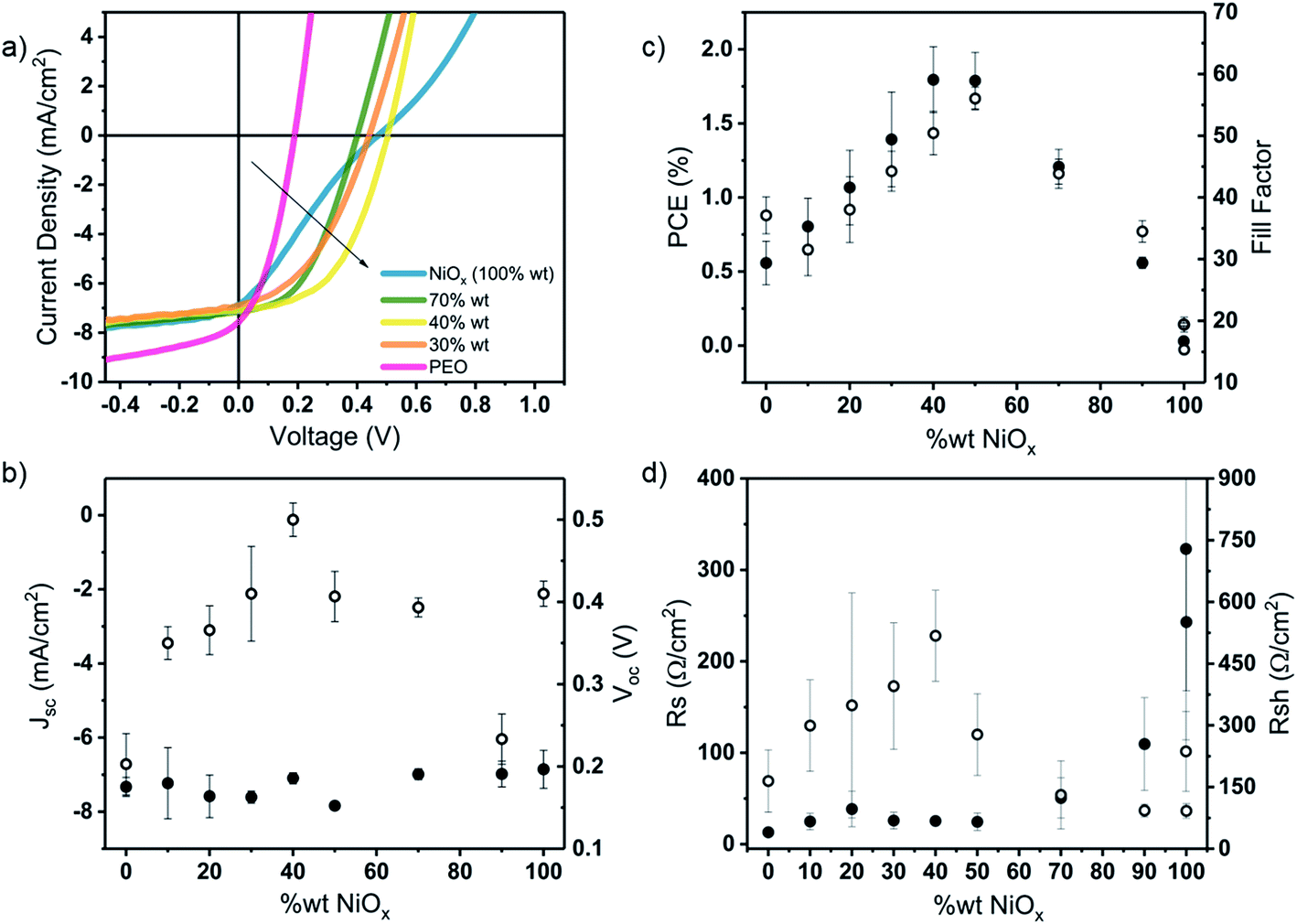 | ||
| Fig. 1 Current density vs. voltage characteristics (a), deduced Jsc (closed circles) and Voc (open circles) (b), deduced PCE (closed circles) and FF (open circles) (c), deduced Rs (closed circles) and Rsh (open circles) (d) of solar cells with the general structure: glass/ITO/NiOx:PEO/P3HT:PC60BM/Ca/Ag as a function of NiOx concentration used to spin-coat the HTL. Curves and data points represent averages of at least eight devices. | ||
From Fig. 1b and c we can deduce that devices with either neat NiOx or PEO HTLs show lower performances than any of the devices with HTLs composed of NiOx:PEO blends. While the short-circuit current (Jsc) is not affected by the HTL, the power conversion efficiency (PCE), fill factor (FF), and open-circuit voltage (Voc) show a bell-shaped dependency with PEO content, with the best overall performance at a NiOx:PEO ratio of 40:60% wt. Through the oxygen plasma treatment, a work function of ≈5.0 eV is obtained independent of the PEO content with exception of the neat PEO on ITO (3.8 eV) (see Fig. S3†). This significantly lower WF in the neat PEO HTL causes an energy level mismatch that leads to a loss in Voc (0.3 V) with respect to that of the best working blend. Devices with a neat NiOx NP HTL are characterized by a distinct S-shape of the JV curve, with substantial losses in FF in comparison to devices with the optimized blend HTL. These losses are commonly attributed to an imbalance in the charge carrier extraction,34,35 suggesting an excessive interface resistance induced by a poor HTL morphology. For the NiOx:PEO blends the presence of PEO seems to be necessary for better photovoltaic performance.
To assess the reason for the bell-shaped efficiency dependency with HTL composition, we extracted the shunt (Rsh) and series resistance (Rs) of all devices, Fig. 1d. We identify two contradicting dependence relationships between blend composition and the device performance which show the best compromise at a NiOx:PEO ratio of 40% wt. In the case of NiOx content >40% wt, the device performance is limited by an increasing Rs. Rs is caused by injection barriers in the device, so we can infer that denser NiOx NP layers are not favorable for efficient hole extraction from the solar cell. In the case of HTL blends with NiOx content <40% wt, Rs values are relatively little affected by composition, however, Rsh strongly depends on composition with a maximum at 40% wt. We conclude that a further decrease in NP concentration < 40% wt does not allow for the formation of a dense nanoparticle layer, thus providing energetically inferior paths for the photocurrent which leads to a decrease of the Rsh and consequently a reduction in the output of the solar cell.
The transient absorption (TA) spectra, after excitation with 500 nm, of P3HT:PCBM films deposited on the optimal 40% wt NiOx:PEO HTL are shown in Fig. 2, while the ones deposited on different NiOx:PEO ratios are depicted in Fig. S4a–c.† At early time delays (0.2 ps), the TA spectra are dominated by the ground state bleaching (GSB) of P3HT below 640 nm, and the stimulated emission (SE) of P3HT excitons centred at 700 nm. At longer time delays (after about 10–20 ps), the SE is replaced by a flat positive band due to charge absorption and the GSB has a significantly reduced amplitude. In agreement with literature,36–38 these spectral changes are due to P3HT exciton dissociation by charge transfer to PCBM. The unusual decrease of the GSB during charge transfer has previously been attributed to a different degree of delocalization of the P3HT excitons and charges.36
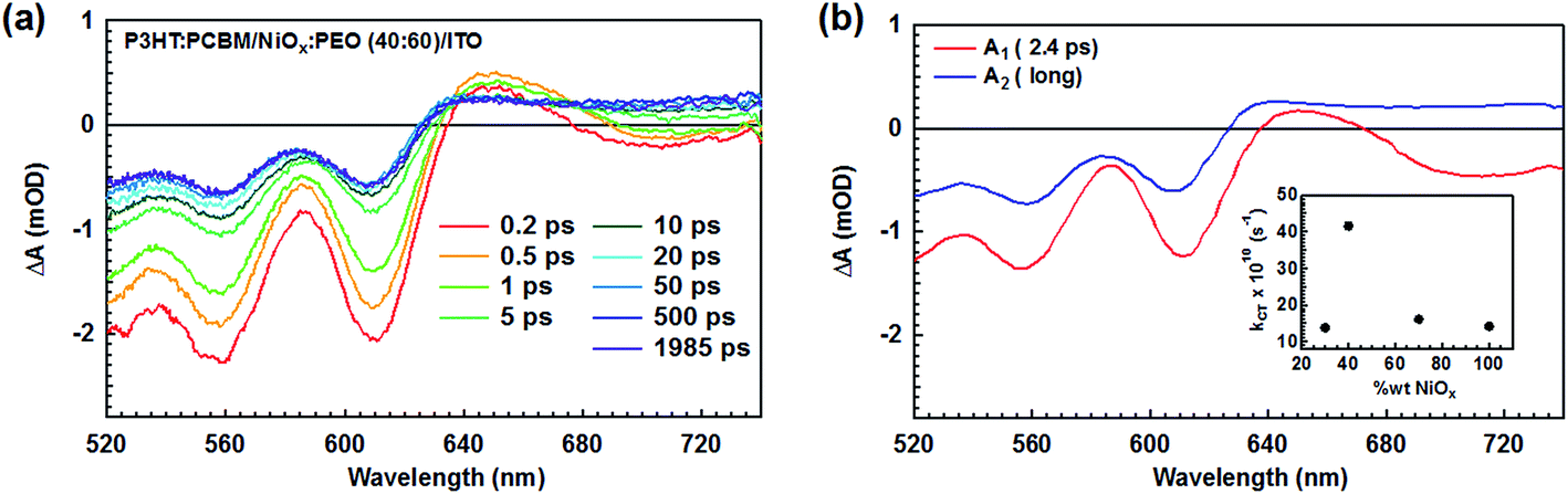 | ||
| Fig. 2 (a) TA Spectra at different time delays after excitation with 500 nm pulses of the HTL with the optimal structure, (b) DAS of the blend with the optimal morphology. The inset shows the charge transfer rate as a function of the % wt of NiOx content. | ||
We have quantified the time constant for the charge transfer by globally analysing the dynamics at all probe wavelengths with an exponential function including an offset. The corresponding amplitude spectra are shown in Fig. 2b and S4d–f,† with the fast component corresponding to the charge transfer and the offset corresponding to long-lived charges. Charge transfer is fastest (2.4 ps) for the 40% wt NiOx:PEO HTL and slower (around 6–7 ps) for the other NiOx:PEO ratios, as illustrated in the inset of Fig. 2b. This points to a slightly modified morphology of the P3HT:PCBM blend with the different HTLs, leading to different time scales for exciton diffusion through P3HT domains before they reach a PCBM interface for dissociation. Although the TA results point to the smallest P3HT domains for the optimal 40% wt NiOx:PEO HTL, the similar absorption spectra of all samples deposited on NiOx:PEO indicate that the aggregation/crystallinity of P3HT remains comparable (Fig. S4g†). Moreover, the charge transfer in all samples is much faster than the exciton lifetime in neat P3HT films (about 400 ps),39,40 so that no significant difference in exciton recombination loss is expected, in agreement with their similar short-circuit current. There is also no sign of charge recombination within the 1 ns experimental time window in any of the samples, showing the absence of fast geminate charge recombination (which would occur within a few nanoseconds).37 We conclude that small morphological changes in P3HT:PCBM are induced by the different HTLs, but that they do not lead to significant differences in the charge generation efficiency that could explain the important changes in device efficiency.
X-ray Photoelectron Spectroscopy (XPS) measurements were performed to investigate the surface chemical composition of the NiOx layers before and after the plasma treatment, as it may strongly influence the interfacial energy alignment with the BHJ material, thereby the final photovoltaic performance. Fig. 3 presents the O 1s, C 1s and Ni 2p XPS spectra for NiOx:PEO HTL with various compositions. Before and after plasma treatment, the spectral distribution of the O 1s and the Ni 2p peaks ascribed to NiOx are not heavily affected, as in previously reported NiOx HTL films prepared by sol–gel methods.19,26 This suggests that the ratio between different oxidation states in the NiOx NPs remains unaltered after plasma treatment. Interestingly, the Ni 2p peak is observed to increase in intensity for the blends while remaining constant for the neat NiOx layer. Simultaneously, the C 1s and the O 1s (534 eV) component of PEO are substantially reduced after plasma treatment. This can be explained by the PEO being etched away – at least partly – during the plasma treatment i.e. decapping the surface of the NiOx NP component. This is corroborated by the improvement in the device performances observed after plasma treatment as shown in Fig. S2.† The XPS characterization and the effect of the plasma treatment on device performances suggest that the main role of the PEO in the blends is to improve the arrangement of the NP in the film, acting as a sacrificial processing additive. Similar device performance improvements have been reported for OPVs with ZnO(NP):poly-vinylpyrrolidone interlayers through surface etching by UV-ozone treatment.41
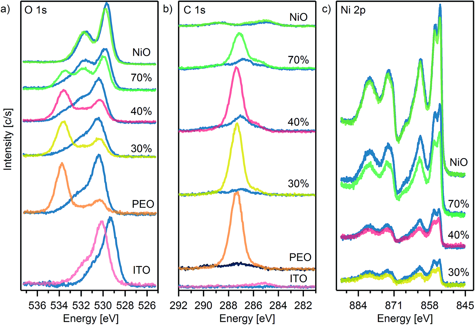 | ||
| Fig. 3 O 1s, C 1s and Ni 2p XPS spectra for ITO, NiOx, PEO, and different NiOx:PEO blends before and after oxygen plasma treatment. Blue trace is the corresponding XPS spectrum after plasma treatment. | ||
The NiOx:PEO HTLs were further investigated by transmission electron microscopy (TEM) and scanning electron microscopy (SEM) with further energy dispersive X-ray spectroscopy (EDS) analysis to clarify the role of PEO in the film formation. Fig. 4a–h shows TEM images of layers of NiOx:PEO with 100%, 70%, 40%, and 30% wt NiOx, where the NPs appear as darker objects dispersed in a bright PEO matrix. The images were acquired on layers thinner than the ones used for devices to avoid imaging disturbance. After plasma treatment, the suspended part of the film was mostly lost due to the etching of PEO and the lack of structural support from the substrate (Fig. S5†). The average interplanar spacing for a NiOx NP, presented in the inset in Fig. 4b, corresponds to the 〈111〉 planes of NiO structure (dhkl = 0.24 nm), confirming the crystalline nature of the NiOx NPs.42–44 The neat NiOx layers (Fig. 4a and b) are dense with several focal planes, indicating the existence of multiple layers of NPs. Blending with PEO causes a gradual dilution and a decrease of the agglomerate sizes of the NPs from an average of ∼55 nm to ∼30 nm as observed in Fig. 4c–h, although some large agglomerates are still present in the blend with 30% wt NiOx.
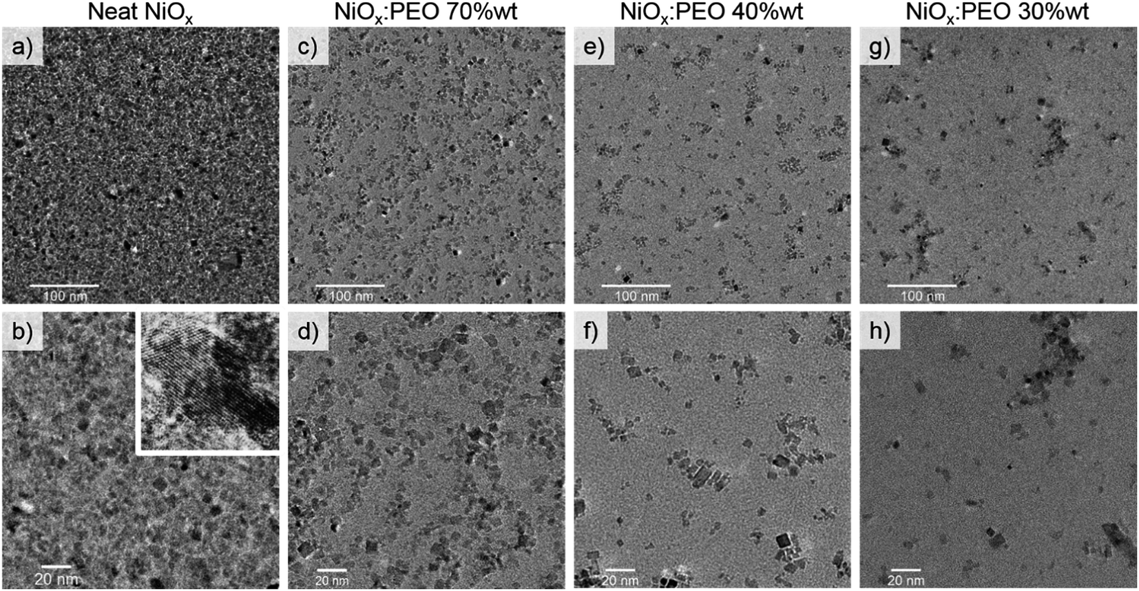 | ||
| Fig. 4 Low magnification (upper panels) and high-magnification (lower panels) TEM images of NiOx:PEO HTLs with different NiOx content. NiOx nanoparticles with diameters of 5–15 nm are observed. The inset (bottom, left panel) shows a close-up image of a single NiOx nanoparticle, the width of the image is 6 nm. | ||
The TEM images show that reducing NiOx content leads to a non-continuity of the HTL (on the nano-scale). At a NiOx NP concentration of 40% wt the coverage is however sufficient to reduce the barrier for charge carrier extraction, effectively screening the effects of the bare areas. Moreover, the nanoscale NP distribution can be directly linked to the resistances in the final devices presented in Fig. 1d. A thick and dense layer of NP, as in the neat NiOx HTLs, causes an increase in the Rs and a decrease in the Rsh, while the separation between the nanoparticles that can be notable depending on the PEO content causes a discontinuity in the HTL that is reflected in the decreased Rsh of the devices.
The surface morphology of the blends on a larger scale was investigated through SEM. Fig. 5 presents the secondary electrons (SE) and back scattered electron (BSE) images of the best working HTL blend (40:60% wt NiOx:PEO) pristine and after plasma treatment. The SE images give information about the surface topography of the film, while the BSE images give additional information on the chemical composition of the sample surface because the contrast depends on the atomic weight, so the Ni-rich zones are bright, and the C-rich zones are dark.
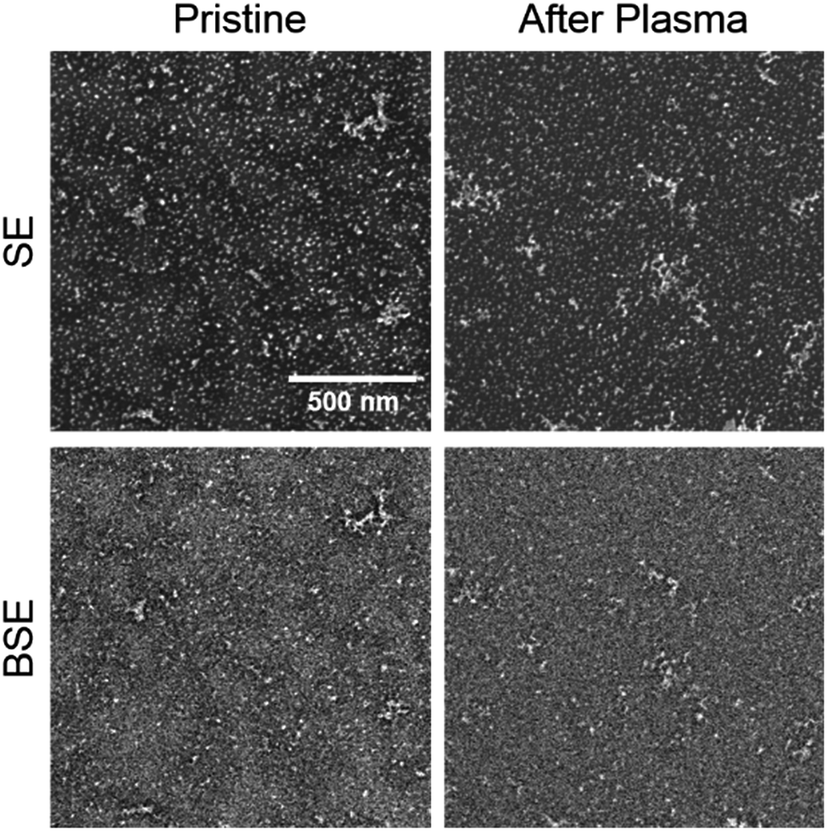 | ||
| Fig. 5 SEM images (SE and BSE modes) of the 40% wt NiOx:PEO HTL, pristine and after plasma treatment. The scale bar corresponds to 500 nm. | ||
The images before plasma treatment show bright NiOx particles and large organic dark “stain” regions indicating a phase separation of the blend components when deposited into a thin layer. After the oxygen plasma treatment, the dark organic “stains” are no longer observable suggesting removal of the PEO leaving behind a NiOx-rich surface. Fig. S6† shows the corresponding images for three other blend compositions reflecting this behavior as well as the neat NiOx HTL.
Element mapping by EDS on SEM images of pristine HTL are displayed in Fig. 6. It can be observed that the continuity and the homogeneity of the NiOx distribution are preserved for the blend layers with 70 and 40% wt NiOx, while HTLs with 30% wt NiOx shows a separation of domains comprised of NiOx-rich islands.
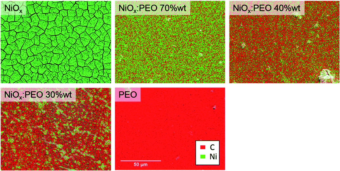 | ||
| Fig. 6 SEM images and EDS mapping of element C (in red) and Ni (in green) of thick NiOx:PEO films with different NiOx content. The cracks on the NiOx film are due to the slow drying process to obtain the desired high thickness required to perform the EDS analysis. The scale bar corresponds to 50 μm. | ||
Finally, devices with inkjet-printed HTL with the optimal blend composition (NiOx 40% wt) were fabricated, after considering the surface wettability (see Fig. S7 and Table S2†) and developing a printable ink formulation. Since the fabrication of layers from ethanol-based solutions is challenging due to the low viscosity and fast evaporation of the solvent (boiling temperature, Tb = 78.4 °C),30,31,45 we incorporated the more viscous diethylene glycol (DEG) (Tb = 197.3 °C) to the as-received NP suspension.
The post-treatments of these layers included vacuum drying, annealing at 100 °C and oxygen plasma treatment. The characteristics of devices fabricated with HTLs from the DEG-containing solutions are displayed in Fig. 7 and relevant parameters are summarized in Table 1. We fabricated spin-coated and inkjet-printed HTLs from the blend as well as neat PEO and NiOx to determine the influence of the printing technique on the device performance. In all cases, the inkjet-printed HTLs resulted in the best performing devices with higher Voc and Jsc, and consequently PCEs. Furthermore, introducing DEG resulted in an improved device performance compared to devices processed from ethanol-only HTLs shown in Fig. 1. Due to its higher boiling point, DEG slows down the drying process, leading to a different film formation dynamics. For the inkjet printing process, a longer drying time provides the necessary time for coalescence of the deposited drops. Notably, the results show that the inclusion of PEO is necessary to obtain the well performing of the NiOx HTLs, with an average PCE = 2.37%. This performance is comparable to the ones obtained in literature with NiOx precursors (sol–gel method) that require a thermal treatment >200 °C.29 Our approach, thus, provides an excellent low-temperature alternative that enables inkjet printing of NiOx HTLs for solution-processed photovoltaics application.
 | ||
| Fig. 7 J–V curves of solar cells with different HTLs prepared by spin coating (dotted line) or inkjet printing (full line). All HTLs were deposited with diethylene glycol as solvent additive. Represented curves are closest to the average of at least four devices. | ||
| J sc (mA cm−2) | V oc (V) | FF | PCE (%) | ||
|---|---|---|---|---|---|
| NiOx | Spin coated | −7.27 ± 0.12 | 0.43 ± 0.01 | 59 ± 3 | 1.87 ± 0.2 |
| Inkjet-printed | −5.20 ± 0.71 | 0.37 ± 0.06 | 34 ± 3 | 0.69 ± 0.2 | |
| NiOx:PEO | Spin coated | −7.09 ± 0.16 | 0.50 ± 0.02 | 50 ± 3 | 1.79 ± 0.2 |
| Inkjet-printed | −7.15 ± 0.23 | 0.54 ± 0.01 | 61 ± 2 | 2.37 ± 0.1 | |
| PEO | Spin coated | −7.33 ± 0.21 | 0.20 ± 0.04 | 37 ± 3 | 0.56 ± 0.1 |
| Inkjet-printed | −6.57 ± 0.40 | 0.31 ± 0.10 | 35 ± 8 | 0.76 ± 0.5 | |
Conclusions
In summary, we demonstrated a low-temperature (100 °C) processing approach for solution-processed NiOx NP-based hole transport layers and its application for organic photovoltaic devices. PEO was utilized as a processing additive, which improves NiOx film formation and can subsequently be removed prior to device fabrication. We showed that an optimal ratio of 40:60% wt between NiOx NP and PEO permits a good dispersion of the nanoparticles without leading to too dense layers that lead to high resistances necessary for maximizing device efficiency. The NiOx:PEO solutions were processed both by spin coating and formulated for use by inkjet printing exhibiting devices performances comparable to precursor-based sol–gel produced NiOx layers that require post-treatments at high temperature. The utilization of P3HT:PCBM as active layer material, although not exhibiting a high performance compared to state-of-the-art organic and perovskites based PVs, offers an optimum standard for the introduction of the presented HTL processing approach. Therefore, we expect that the low-temperature process reported here by blending NiOx with a sacrificial polymer additive can be applicable to a wider range of hybrid systems and interfaces in multilayer optoelectronic devices resulting in device architectures more suitable for the industrial processing of printed devices on plastic substrates.
Conflicts of interest
There are no conflicts of interest to declare.Statement of contribution
M. R. prepared all the samples and characterized films and devices. G. H. S. provided interpretation of device data. A. L. and T. S. performed TEM, SEM and EDS characterization, G. L. F. provided interpretation of scanning microscopy data. G. M. M. performed optical transmission, optical microscopy and contact angle measurements. N. D. performed the transient absorption analysis, N. B. provided interpretation of transient absorption spectra. S. S. and E. S. performed inkjet printing experiments and the surface free energy characterization. P. R. and E. M. performed XPS experiments. M. R., W. K., N. S. and G. H. S. developed concept and planned experiments. M. R., N. S., N. B., G. L. F. and G. H. S. wrote the manuscript. All authors approved the final manuscript and provided feedback.Acknowledgements
This work was financially supported by the EC through the Horizon 2020 Marie Skłodowska-Curie ITN project INFORM (Grant Agreement 675867). The authors thank N. Strobel and M. Dyson for fruitful discussion.Reference
- X. Li, W. Zhang, K. Usman and J. Fang, Small Molecule Interlayers in Organic Solar Cells, Adv. Energy Mater., 2018, 8(28), 1702730, DOI:10.1002/aenm.201702730.
- S. Sato, S. Ohisa, Y. Hayashi, R. Sato, D. Yokoyama, T. Kato, M. Suzuki, T. Chiba, Y.-J. Pu and J. Kido, Air-Stable and High-Performance Solution-Processed Organic Light-Emitting Devices Based on Hydrophobic Polymeric Ionic Liquid Carrier-Injection Layers, Adv. Mater., 2018, 30(18), 1705915, DOI:10.1002/adma.201705915.
- T. Chiba, Y.-J. Pu and J. Kido, Solution-Processable Electron Injection Materials for Organic Light-Emitting Devices, J. Mater. Chem. C, 2015, 3(44), 11567–11576, 10.1039/c5tc02421h.
- X. Yu, T. J. Marks and A. Facchetti, Metal Oxides for Optoelectronic Applications, Nat. Mater., 2016, 15(4), 383–396, DOI:10.1038/nmat4599.
- C. Glynn and C. O'Dwyer, Solution Processable Metal Oxide Thin Film Deposition and Material Growth for Electronic and Photonic Devices, Adv. Mater. Interfaces, 2017, 4, 1600610 CrossRef.
- W. C. H. Choy and D. Zhang, Solution-Processed Metal Oxides as Efficient Carrier Transport Layers for Organic Photovoltaics, Small, 2016, 12(4), 416–431, DOI:10.1002/smll.201502258.
- M. Ruscello, S. Stolz, D. L. Gonzalez Arellano, F. Ullrich, S. Hillebrandt, E. Mankel, A. Pucci, W. Kowalsky, T. Emrick and A. L. Briseno, et al., Electron Injection and Interfacial Trap Passivation in Solution-Processed Organic Light-Emitting Diodes Using a Polymer Zwitterion Interlayer, Org. Electron., 2017, 50, 384–388, DOI:10.1016/j.orgel.2017.08.014.
- T. H. Lai, S. W. Tsang, J. R. Manders, S. Chen and F. So, Properties of Interlayer for Organic Photovoltaics, Mater. Today, 2013, 16(11), 424–432, DOI:10.1016/j.mattod.2013.10.001.
- S. Stolz, M. Petzoldt, S. Dück, M. Sendner, U. H. F. Bunz, U. Lemmer, M. Hamburger and G. Hernandez-Sosa, High-Performance Electron Injection Layers with a Wide Processing Window from an Amidoamine-Functionalized Polyfluorene, ACS Appl. Mater. Interfaces, 2016, 8(20), 12959–12967, DOI:10.1021/acsami.6b03557.
- Z. Yin, J. Wei and Q. Zheng, Interfacial Materials for Organic Solar Cells: Recent Advances and Perspectives, Adv. Sci., 2016, 3(8), 1–37, DOI:10.1002/advs.201500362.
- S. Shao, K. Zheng, T. Pullerits and F. Zhang, Enhanced Performance of Inverted Polymer Solar Cells by Using Poly(Ethylene Oxide)-Modified ZnO as an Electron Transport Layer, ACS Appl. Mater. Interfaces, 2013, 5(2), 380–385, DOI:10.1021/am302408w.
- O. Malinkiewicz, A. Yella, Y. H. Lee, G. M. M. Espallargas, M. Graetzel, M. K. Nazeeruddin and H. J. Bolink, Perovskite Solar Cells Employing Organic Charge-Transport Layers, Nat. Photonics, 2014, 8, 128–132, DOI:10.1038/nphoton.2013.341.
- S. B. Jo, J. H. Lee, M. Sim, M. Kim, J. H. Park, Y. S. Choi, Y. Kim, S. G. Ihn and K. Cho, High Performance Organic Photovoltaic Cells Using Polymer-Hybridized ZnO Nanocrystals as a Cathode Interlayer, Adv. Energy Mater., 2011, 1(4), 690–698, DOI:10.1002/aenm.201100154.
- F. Wang, Z. Tan and Y. Li, Solution-Processable Metal Oxides/Chelates as Electrode Buffer Layers for Efficient and Stable Polymer Solar Cells, Energy Environ. Sci., 2015, 8(4), 1059–1091, 10.1039/c4ee03802a.
- S. Chen, J. R. Manders, S.-W. Tsang and F. So, Metal Oxides for Interface Engineering in Polymer Solar Cells, J. Mater. Chem., 2012, 24202–24212, 10.1039/c2jm33838f.
- K. Zilberberg, J. Meyer and T. Riedl, Solution Processed Metal-Oxides for Organic Electronic Devices, J. Mater. Chem. C, 2013, 1(32), 4796, 10.1039/c3tc30930d.
- M. T. Greiner, M. G. Helander, Z. B. Wang, W. M. Tang and Z. H. Lu, Effects of Processing Conditions on the Work Function and Energy-Level Alignment of NiO Thin Films, J. Phys. Chem. C, 2010, 114(46), 19777–19781, DOI:10.1021/jp108281m.
- S. Hietzschold, S. Hillebrandt, F. Ullrich, J. Bombsch, V. Rohnacher, S. Ma, W. Liu, A. Köhn, W. Jaegermann and A. Pucci, et al., Functionalized Nickel Oxide Hole Contact Layers: Work Function versus Conductivity, ACS Appl. Mater. Interfaces, 2017, 9(45), 39821–39829, DOI:10.1021/acsami.7b12784.
- F. Ullrich, S. Hillebrandt, S. Hietzschold, V. Rohnacher, T. Marszalek, W. Kowalsky, R. Lovrincic, S. Beck, E. Mankel and A. Pucci, Correlation between Chemical and Electronic Properties of Solution-Processed Nickel Oxide, ACS Appl. Energy Mater., 2018, 1(7), 3113–3122, DOI:10.1021/acsaem.8b00284.
- Y. Hou, W. Chen, D. Baran, T. Stubhan, N. A. Luechinger, B. Hartmeier, M. Richter, J. Min, S. Chen and C. O. R. Quiroz, et al., Overcoming the Interface Losses in Planar Heterojunction Perovskite-Based Solar Cells, Adv. Mater., 2016, 5112–5120, DOI:10.1002/adma.201504168.
- W. Yang, Z. Yu, W. Liu, C.-Z. Li and H. Chen, Aqueous Solution-Processed NiO x Anode Buffer Layers Applicable for Polymer Solar Cells, J. Polym. Sci., Part A: Polym. Chem., 2017, 55(4), 747–753, DOI:10.1002/pola.28427.
- F. Jiang, W. C. H. Choy, X. Li, D. Zhang and J. Cheng, Post-Treatment-Free Solution-Processed Non-Stoichiometric NiOx Nanoparticles for Efficient Hole-Transport Layers of Organic Optoelectronic Devices, Adv. Mater., 2015, 27(18), 2930–2937, DOI:10.1002/adma.201405391.
- Y. Wei, K. Yao, X. Wang, Y. Jiang, X. Liu, N. Zhou and F. Li, Improving the Efficiency and Environmental Stability of Inverted Planar Perovskite Solar Cells via Silver-Doped Nickel Oxide Hole-Transporting Layer, Appl. Surf. Sci., 2018, 427, 782–790, DOI:10.1016/j.apsusc.2017.08.184.
- J. Cheng, X. Ren, H. L. Zhu, J. Mao, C. Liang, J. Zhuang, V. A. L. Roy and W. C. H. Choy, Pre- and Post-Treatments Free Nanocomposite Based Hole Transport Layer for High Performance Organic Solar Cells with Considerably Enhanced Reproducibility, Nano Energy, 2017, 34, 76–85, DOI:10.1016/j.nanoen.2017.02.021.
- H. Lee, E. Puodziukynaite, Y. Zhang, J. C. Stephenson, L. J. Richter, D. a Fischer, D. M. Delongchamp, T. Emrick and A. L. Briseno, Poly(Sulfobetaine Methacrylate)s as Electrode Modi Fi Ers for Inverted Organic Electronics, J. Am. Chem. Soc., 2015, 137, 540–549, DOI:10.1021/ja512148d.
- E. L. Ratcliff, J. Meyer, K. X. Steirer, A. Garcia, J. J. Berry, D. S. Ginley, D. C. Olson, A. Kahn and N. R. Armstrong, Evidence for Near-Surface NiOOH Species in Solution-Processed NiOx Selective Interlayer Materials: Impact on Energetics and the Performance of Polymer Bulk Heterojunction Photovoltaics, Chem. Mater., 2011, 23(22), 4988–5000, DOI:10.1021/cm202296p.
- H. Hu, J. Zhu, M. Chen, T. Guo and F. Li, Inkjet-Printed p-Type Nickel Oxide Thin-Film Transistor, Appl. Surf. Sci., 2018, 441, 295–302, DOI:10.1016/j.apsusc.2018.02.049.
- R. Brisse, R. Faddoul, T. Bourgeteau, D. Tondelier, J. Leroy, S. Campidelli, T. Berthelot, B. Geffroy and B. Jousselme, Inkjet Printing NiO-Based p-Type Dye-Sensitized Solar Cells, ACS Appl. Mater. Interfaces, 2017, 9(3), 2369–2377, DOI:10.1021/acsami.6b12912.
- A. Singh, S. K. Gupta and A. Garg, Inkjet Printing of NiO Films and Integration as Hole Transporting Layers in Polymer Solar Cells, Sci. Rep., 2017, 7(1), 1775, DOI:10.1038/s41598-017-01897-9.
- G. Cummins and M. P. Y. Desmulliez, Inkjet Printing of Conductive Materials: A Review, Circuit World, 2012, 38(4), 193–213, DOI:10.1108/03056121211280413.
- J. S. Gebauer, V. Mackert, S. Ognjanović and M. Winterer, Tailoring Metal Oxide Nanoparticle Dispersions for Inkjet Printing, J. Colloid Interface Sci., 2018, 526, 400–409, DOI:10.1016/j.jcis.2018.05.006.
- M. Jlassi, I. Sta, M. Hajji and H. Ezzaouia, Optical and Electrical Properties of Nickel Oxide Thin Films Synthesized by Sol–Gel Spin Coating, Mater. Sci. Semicond. Process., 2014, 21(1), 7–13, DOI:10.1016/j.mssp.2014.01.018.
- H. Zhang, J. Cheng, F. Lin, H. He, J. Mao, K. S. Wong, A. K. Y. Jen and W. C. H. Choy, Pinhole-Free and Surface-Nanostructured Niox Film by Room-Temperature Solution Process for High-Performance Flexible Perovskite Solar Cells with Good Stability and Reproducibility, ACS Nano, 2016, 10(1), 1503–1511, DOI:10.1021/acsnano.5b07043.
- B. Ecker, H. J. Egelhaaf, R. Steim, J. Parisi and E. Von Hauff, Understanding S-Shaped Current–Voltage Characteristics in Organic Solar Cells Containing a TiOx Interlayer with Impedance Spectroscopy and Equivalent Circuit Analysis, J. Phys. Chem. C, 2012, 116(31), 16333–16337, DOI:10.1021/jp305206d.
- J. C. Wang, X. C. Ren, S. Q. Shi, C. W. Leung and P. K. L. Chan, Charge Accumulation Induced S-Shape J–V Curves in Bilayer Heterojunction Organic Solar Cells, Org. Electron., 2011, 12(6), 880–885, DOI:10.1016/j.orgel.2011.02.016.
- R. A. Marsh, J. M. Hodgkiss, S. Albert-Seifried and R. H. Friend, Effect of Annealing on P3HT:PCBM Charge Transfer and Nanoscale Morphology Probed by Ultrafast Spectroscopy, Nano Lett., 2010, 10(3), 923–930, DOI:10.1021/nl9038289.
- I. A. Howard, R. Mauer, M. Meister and F. Laquai, Effect of Morphology on Ultrafast Free Carrier Generation in Polythiophene:Fullerene Organic Solar Cells, J. Am. Chem. Soc., 2010, 132(42), 14866–14876, DOI:10.1021/ja105260d.
- J. Guo, H. Ohkita, H. Benten and S. Ito, Charge Generation and Recombination Dynamics in Poly(3-Hexylthiophene)/Fullerene Blend Films with Different Regioregularities and Morphologies, J. Am. Chem. Soc., 2010, 132(17), 6154–6164, DOI:10.1021/ja100302p.
- N. Banerji, S. Cowan, E. Vauthey and A. J. Heeger, Ultrafast Relaxation of the Poly(3-Hexylthiophene) Emission Spectrum, J. Phys. Chem. C, 2011, 115(19), 9726–9739, DOI:10.1021/jp1119348.
- S. Cook, A. Furube and R. Katoh, Analysis of the Excited States of Regioregular Polythiophene P3HT, Energy Environ. Sci., 2008, 1(2), 294, 10.1039/b805643a.
- C. E. Small, S. Chen, J. Subbiah, C. M. Amb, S. W. Tsang, T. H. Lai, J. R. Reynolds and F. So, High-Efficiency Inverted Dithienogermole-Thienopyrrolodione-Based Polymer Solar Cells, Nat. Photonics, 2012, 6(2), 115–120, DOI:10.1038/nphoton2011317.
- H. L. Chen, Y. M. Lu and W. S. Hwang, Characterization of Sputtered NiO Thin Films, Surf. Coat. Technol., 2005, 198(1–3), 138–142, DOI:10.1016/j.surfcoat.2004.10.032.
- J. Zhang, J. Wang, Y. Fu, B. Zhang and Z. Xie, Efficient and Stable Polymer Solar Cells with Annealing-Free Solution-Processible NiO Nanoparticles as Anode Buffer Layers, J. Mater. Chem. C, 2014, 2(39), 8295–8302, 10.1039/c4tc01302f.
- U. Kwon, B.-G. Kim, D. C. Nguyen, J.-H. Park, N. Y. Ha, S.-J. Kim, S. H. Ko, S. Lee, D. Lee and H. J. Park, Solution-Processible Crystalline NiO Nanoparticles for High-Performance Planar Perovskite Photovoltaic Cells, Sci. Rep., 2016, 6(1), 30759, DOI:10.1038/srep30759.
- X. Liu, T. J. Tarn, F. Huang and J. Fan, Recent Advances in Inkjet Printing Synthesis of Functional Metal Oxides, Particuology, 2015, 19, 1–13, DOI:10.1016/j.partic.2014.05.001.
Footnote |
| † Electronic supplementary information (ESI) available. See DOI: 10.1039/c9se00216b |
| This journal is © The Royal Society of Chemistry 2019 |