
 Open Access Article
 This Open Access Article is licensed under a
 Creative Commons Attribution 3.0 Unported Licence
Photoelectrochemical water oxidation of GaP1−xSbx with a direct band gap of 1.65 eV for full spectrum solar energy harvesting†
Mahdi
Alqahtani
 ab,
Sanjayan
Sathasivam
c,
Lipin
Chen
d,
Pamela
Jurczak
a,
Rozenn
Piron
d,
Christophe
Levallois
d,
Antoine
Létoublon
d,
Yoan
Léger
d,
Soline
Boyer-Richard
d,
Nicolas
Bertru
d,
Jean–Marc
Jancu
d,
Charles
Cornet
*d,
Jiang
Wu
*a and
Ivan P.
Parkin
*c
ab,
Sanjayan
Sathasivam
c,
Lipin
Chen
d,
Pamela
Jurczak
a,
Rozenn
Piron
d,
Christophe
Levallois
d,
Antoine
Létoublon
d,
Yoan
Léger
d,
Soline
Boyer-Richard
d,
Nicolas
Bertru
d,
Jean–Marc
Jancu
d,
Charles
Cornet
*d,
Jiang
Wu
*a and
Ivan P.
Parkin
*c
aDepartment of Electronic and Electrical Engineering, University College London, London WC1E 7JE, UK. E-mail: jiangwu@uestc.edu.cn
bKing Abdulaziz City for Science and Technology (KACST), Riyadh 12371, Saudi Arabia. E-mail: i.p.parkin@ucl.ac.uk
cDepartment of Chemistry, University College London, London WC1H 0AJ, UK
dUniv Rennes, INSA Rennes, CNRS, Institut FOTON – UMR 6082, F-35000 Rennes, France. E-mail: charles.cornet@insa-rennes.fr
First published on 3rd April 2019
Abstract
Hydrogen produced using artificial photosynthesis, i.e. solar splitting of water, is a promising energy alternative to fossil fuels. Efficient solar water splitting demands a suitable band gap to absorb near full spectrum solar energy and a photoelectrode that is stable in strongly alkaline or acidic electrolytes. In this work, we demonstrate for the first time, a perfectly relaxed GaP0.67Sb0.33 monocrystalline alloy grown on a silicon substrate with a direct band gap of 1.65 eV by molecular beam epitaxy (MBE) without any evidence of chemical disorder. Under one Sun illumination, the GaP0.67Sb0.33 photoanode with a 20 nm TiO2 protective layer and 8 nm Ni co-catalyst layer shows a photocurrent density of 4.82 mA cm−2 at 1.23 V and an onset potential of 0.35 V versus the reversible hydrogen electrode (RHE) in 1.0 M KOH (pH = 14) aqueous solution. The photoanode yields an incident-photon-to-current efficiency (IPCE) of 67.1% over the visible range between wavelengths 400 nm to 650 nm. Moreover, the GaP0.67Sb0.33 photoanode was stable over 5 h without degradation of the photocurrent under strong alkaline conditions under continuous illumination at 1 V versus RHE. Importantly, the direct integration of the 1.65 eV GaP0.67 Sb0.33 on 1.1 eV silicon may pave the way for an ideal tandem photoelectrochemical system with a theoretical solar to hydrogen efficiency of 27%.
Introduction
The combustion of fossil fuels such as coal and oil is recognised as one of the major sources of climate change due to the emission of greenhouse gasses such as carbon dioxide. Due to the impact of global warming on society, there is an urgent need to find alternative energy sources that are clean, renewable, and abundant.1 In this regard, the photoelectrochemical (PEC) splitting of water to oxygen and hydrogen using solar radiation is considered as a promising technology.2,3 To fulfil the sustainable energy objective, PEC systems need to be a cost-effective, stable in strongly alkaline or acidic electrolytes, and harvest a large portion of the solar spectrum. Despite the high solar-to-hydrogen conversion efficiency of monolithic photovoltaic-biased PEC cells and multiple absorbers, the complexity of their fabrication and prohibitive cost hinder their use for large-scale applications.4–6 For metal oxides, large band gaps (usually larger than 2 eV) limit solar light absorption which typically leads to a lower solar to hydrogen (STH) conversion efficiency.7,8 In that case, using a single photoelectrode, i.e., one absorber photoelectrode, with a direct band gap (ideally 1.6 eV) provides a desirable and potentially low-cost approach due to a balanced combination of simplicity in fabrication and efficient photon harvesting for PEC water splitting. For example, a single semiconductor with a band gap of 1.6 eV can yield a maximum solar-to-hydrogen (STH) efficiency of 30% under one sun illumination.2 However, due to the relatively high overpotential and the requirement of four holes per oxygen molecule, the water oxidation process presents a bottleneck for realization of efficient and practical water splitting systems. Therefore, the development of high-performance PEC water splitting systems has been hindered due to the lack of an ideal photoanode material that has a sufficiently narrow bandgap and is stable under strongly alkaline or acidic conditions. On the other hand, it is well known that the band edges of III–V semiconductor alloys, are adjustable by controlling their composition, such that the band gap of GaP1−xSbx can be tuned from 2.26 eV (bandgap of GaP) to 0.72 eV (bandgap of GaSb).9 More importantly, GaP1−xSbx with a band gap of 1.6–2.3 eV is a promising top absorber on a Si (1.1 eV) bottom absorber that may pave the way for ideal tandem PEC systems corresponding to a theoretical solar to hydrogen efficiency of 27%.10 For instance, Sunkara et al. have demonstrated that GaP with 3% antimony being incorporated, has a direct bandgap of 2.68 eV that enhances the absorption spectrum but leads to relatively low photocurrent density due to the large bandgap. However, it is commonly known that growing a high-quality structure of GaP with a high content of Sb on a silicon substrate is challenging, due to the large lattice mismatch. Furthermore, the stability of III–V semiconductor photoanodes for water oxidation is a critical challenge when operated in contact with aqueous solutions.Protective layers and catalysts can stabilize the photoanodes by reducing the kinetic overpotential and prevent the accumulation of holes at the semiconductor photoelectrode surface in strongly alkaline solution. Titanium dioxide (TiO2), is one of the best layers to protect the surfaces of III–V materials from photocorrosion. The strategy uses either an ultra-thin layer to allow the charge transfer via tunnelling9 or a “leaky” defect-state formed in a thicker TiO2 layer11 due to the high intrinsic chemical stability.12,13 Metallic oxygen evolution reaction (OER) catalysts, such as Ni, are earth-abundant catalysts that facilitate the efficient water oxidation in strong alkaline solution.14
In this work, for the first time we fabricated GaP1−xSbx on a silicon substrate by molecular beam epitaxy (MBE) with a high concentration of Sb (x = 0.33) that allows the band gap to be reduced to a direct bandgap of 1.65 eV. By using an atomic-layer deposition (ALD) grown-TiO2 (20 nm) as the protection layer and Ni (8 nm) as an oxygen evolution co-catalyst, the GaP0.67Sb0.33 photoanode exhibited a high photocurrent density of 4.82 mA cm−2 at 1.23 V and an onset potential of 0.35 V versus the reversible hydrogen electrode (RHE) in 1.0 M KOH (pH = 14) electrolyte under one sun illumination. The narrow bandgap of the GaP0.67Sb0.33 photoanode leads to an incident-photon-to-current efficiency (IPCE) value of 67.1% for wavelengths 400 nm to 650 nm. Moreover, the GaP0.67Sb0.33 photoanode was stable for 5 h without degradation in the photocurrent under strong alkaline conditions under continuous illumination at 1 V versus RHE.
Results and discussion
The structural properties of the GaP0.67Sb0.33 photoanode were analysed by scanning transmission electron microscopy (STEM). The cross-sectional STEM images in both low and high magnification of the nominally undoped 1 μm-thick GaP0.67Sb0.33 grown on a Si substrate photoanode used for PEC water splitting are shown in Fig. 1a. It shows the presence of numerous crystal twins, originating from the GaP0.67Sb0.33/Si interface, which introduce non-optimized growth initiation steps.12,14 Nevertheless, the structural quality of the GaP0.67Sb0.33 grown on a Si substrate is much improved compared with previous studies.15,16 As shown later, it is remarkable that despite the presence of these crystal defects, and the absence of intentional doping, the photocurrent of the GaP0.67Sb0.33 grown on Si photoanode remains high compared to a reference n-doped GaP photoanode (see Fig. S7 in the ESI†) (with a much lower density of crystal defects). This behaviour is related to the presence of emerging antiphase boundaries (APBs) in the structure. Indeed, common strategies to annihilate APBs9,17 were not used to grow this sample, resulting in APBs propagating over the whole volume of the GaP0.67Sb0.33 epilayer, as shown in Fig. 1a. This results in an average unintentional n-doping level of 1018 cm−3, acting as electrical shunts in the structure.18,19 Photogenerated carriers in the GaP0.67Sb0.33 epilayer are then brought to the surface or to the GaP0.67Sb0.33/Si interface more easily. Finally, the presence of APBs is also expected to create intermediate bandgap energy levels.20–22 STEM energy dispersive X-ray spectroscopy (EDS) measurements were carried out for elemental composition extraction. Chemical analysis of the GaP0.67Sb0.33 on the Si photoanode is shown in Fig. 1b. Elemental profiles of the GaP0.67Sb0.33/Si interface are plotted for the involved chemical species (Si, Ga, P and Sb). They show that the projected interface between GaP0.67Sb0.33 and Si is relatively well defined, with an apparent intermixing layer of around 5 nm at most. This transition area is more likely due to the residual roughness of the Si substrate, than due to real GaP0.67Sb0.33 on Si intermixing.21Fig. 1b also shows that the P and Sb contents are stable within the layer, indicating an overall composition homogeneity of the sample, within the EDS resolution. The XPS analysis of the surface also shows the formation of a very standard GaP0.67Sb0.33-based native oxide (see Fig. S1, ESI†). Fig. 1c presents the results of X-ray diffraction (XRD) analysis on the GaP0.67Sb0.33 grown on a Si substrate. A miscut of 6.1 ± 0.05° is observed toward the [110] direction, from the positions of the Si Bragg peaks, in agreement with the substrate specifications. The scan exhibits a well-defined GaP0.67Sb0.33 Bragg peak. Reciprocal space maps carried out on either (224) (Fig. 1c inset) or (004) reflections (see Fig. S2, ESI†) show a full plastic relaxation of the GaP0.67Sb0.33 layer. Very similar values of the GaP0.67Sb0.33 lattice parameter have been extracted from both the RSM and
  scan, confirming the full plastic relaxation rate and giving a mean lattice parameter of 0.5665 ± 0.0005 nm. The antimony content in GaP0.67Sb0.33X = 0.33 ± 0.01 is then inferred from these values.15 The observed position of the GaP0.67Sb0.33 peak overlaps the relaxation line (bold dashed line in the inset). This actually corresponds to a supplementary tilt of the order of 0.4°. This is classically interpreted as the contribution of the miscut on the plastic relaxation process. A Δα Nagai angle of 0.25° is calculated as:
 | (1) |
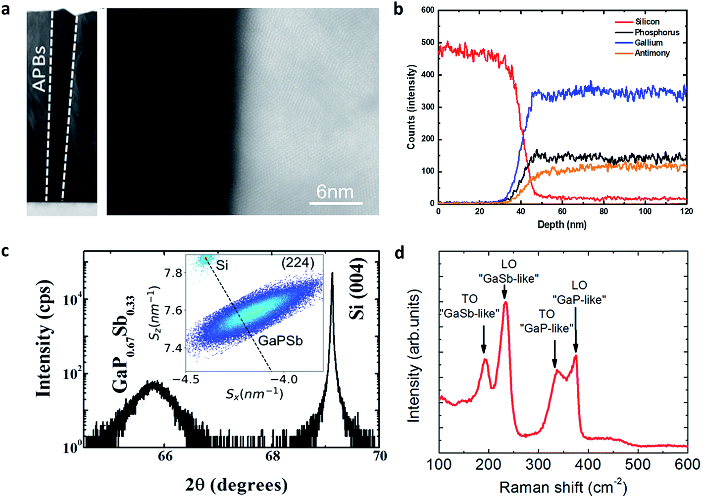 | ||
| Fig. 1 Structural characterization of the GaP0.67Sb0.33 photoanode. (a) The cross-sectional high-resolution STEM images of GaP0.67Sb0.33 grown on a Si substrate. (b) Si, Ga, Sb, and P concentration depth profiles for GaP0.67Sb0.33 grown on a silicon substrate using energy dispersive X-ray spectroscopy (EDS). (c) X-ray diffraction ω/2θ scan performed in the vicinity of the Si (004) Bragg reflection showing the distant GaP0.67Sb0.33 peak. The inset shows the reciprocal space map around (224) illustrating the full relaxation state of GaP0.67Sb0.33 (Sx and Sz are the projected coordinates in the right handed Cartesian, with the z axis parallel to the surface normal).43 (d) Raman scattering spectrum of the GaP0.67Sb0.33 photoanode showing the two-mode (GaP-like and GaSb-like) structuration, composed of both LO and TO phonons. | ||
To further investigate the electronic properties of the GaP0.67Sb0.33 grown on Si photoanode, the band structure of the unstrained GaP0.67Sb0.33 alloy was calculated using a tight-binding method, with an extended basis sp3d5s* tight binding Hamiltonian;26 this is shown in Fig. 2a. The bandgaps obtained in the Γ, L and X valleys are respectively 1.753, 1.784 and 2.071 eV at 0 K. The alloy therefore has a direct bandgap band structure. The value found in these calculations is in good agreement with the one determined from the absorption spectrum deduced by ellipsometry measurements at 300 K (see Fig. S3, ESI†) (1.65 eV), considering a conventional 50–70 meV temperature shift. It is also consistent with the IPCE curve presented in Fig. 4c that shows significant photocurrent generation just below 750 nm. Finally, the bandgap determined in this study is also in agreement with pioneering studies on GaP1−xSbx of Loualiche et al.27 Water redox potentials of H+/H2 and O2/H2O are relatively positioned as marked by black dashed lines in Fig. 2a, with respect to the GaP0.67Sb0.33 alloy valence band. To do this, we have used the absolute band line-up between GaP and GaSb28 and the absolute band line-ups between GaP and the water redox potentials.29 An energy shift of 0.41 eV is needed to align the valence band maximum and the O2/H2O energy level, as illustrated by the blue dashed lines in Fig. 2a. In the present study, the large band bending in the GaP0.67Sb0.33 grown on a Si substrate cannot be predicted accurately, because of the surface pinning and the presence of APBs. Therefore, the advantages of GaP0.67Sb0.33 through accurate monitoring of the Sb content, as compared to GaP, extends the absorption spectral range and direct band gap transition.
 | ||
| Fig. 2 Electronic and optical properties of the GaP0.67Sb0.33 photoanode. (a) Band structure of the bulk unstrained GaP0.67Sb0.33 at 0 K. Bandgaps of 1.753, 1.784 and 2.071 eV are respectively computed for the Γ, L and X valleys. Relative positions of the water redox potentials are superimposed. (b) Temperature-dependent photoluminescence spectra between 15 K and 150 K showing a large Stokes shift, evidencing carrier localization. The inset shows the corresponding Arrhenius plot for the two transitions, being the Low Energy Line (LEL) and High Energy Line (HEL). | ||
The optical properties of the GaP0.67Sb0.33 photoanode were further studied using photoluminescence (PL) spectroscopy, as shown in Fig. 2b. Fig. 2b shows the temperature dependent PL analysis on this sample. The PL signal was detected up to 150 K. At first, two transitions are clearly distinguishable, at respectively 1.22 eV (Low Energy Line-LEL), and 1.38 eV (High Energy Line-HEL). From the experimental absorption curve presented in Fig. 4c, and calculations presented in Fig. 2a, the emission properties of the sample cannot be attributed to the bandgap of the bulk GaP0.67Sb0.33 (that lies around 1.7 eV at low temperature). This strong Stokes shift is necessarily a consequence of deep carrier localisation in the GaP0.67Sb0.33 layer. The PL peaks were fitted by using a two-component Gaussian curve to deduce the Arrhenius evolutions for each PL peak, as shown in Fig. 2b inset. The fitting of Arrhenius evolutions requires 3 activation energies which are identical for the two lines: 8 meV, 30 meV and 130 meV. The first one is attributed to a small alloy disorder, while the other two represent the detrapping of localized carriers to extended states. Interestingly, if the photoluminescence is not robust with increasing temperature, the 15 K PL intensity is significantly larger than the one usually measured in GaP-based quantum dots or quantum wells that are of the indirect type.30 We therefore conclude that this PL signal comes from localization of excitons in the sample, with a direct bandgap. However, due to the various crystal defects shown in Fig. 1, the non-radiative lifetime is short, and redistribution of carriers to the non-radiative centres hampers the observation of room temperature PL. It is worth noting that localization of carriers around non-radiative or radiative centres does not prevent good operation of the photoanode. The presence of antiphase boundaries, acting as preferential transport channels (and thus preventing the carriers from approaching non-radiative centres) may again explain this observation.
Fig. 3a and b show the schematic diagram of the structure for the GaP0.67Sb0.33 photoanode coated with a protection layer TiO2 after being combined with the Ni co-catalyst. The experimental setup that was used for the photoelectrochemical measurements consisted of a working electrode (GaP0.67Sb0.33), reference electrode (Ag/AgCl), and counter electrode (platinum coil). The PEC performance of GaP0.67Sb0.33 photoanodes were investigated using a standard three-electrode configuration in 1.0 M KOH electrolyte (pH = 14) under one sun illumination. The photocurrent density–voltage (J–V) curve for the GaP0.67Sb0.33 without a coated photoanode is shown in Fig. 3c. Under AM 1.5G simulated one sun illumination, it shows that the onset potential for GaP0.67Sb0.33 without the photoanode coating is 0.4 V versus the reversible hydrogen electrode (RHE) and this onset potential correlates with the flat band potential of the photoanode which is also determined by Mott–Schottky measurements in Fig. 3d. The saturated photocurrent density was 13.26 mA cm−2 at 1.23 V versus the reversible hydrogen electrode (RHE). In addition, to determine the flat band potentials of the GaP0.67Sb0.33 without the photoanode coating and donor concentration, we performed Mott–Schottky measurements in three electrode configurations in 1.0 M KOH (pH = 14) as shown in Fig. 3d. The slope is positive which indicates the electrode is an n-type material. The flat band potential (VFB) and the donor concentration were 0.5 V and 3.86 × 1015 cm−3versus RHE, respectively (see the Experimental section). On the other hand, an ALD-TiO2 of 20 nm thickness was deposited directly onto the surface of the GaP0.67Sb0.33 photoanode as a protection layer from photocorrosion. Metallic nickel (Ni) 8 nm was deposited onto the surface of the GaP0.67Sb0.33–TiO2 photoanode as a co-catalyst using a thermal evaporator (see Materials characterisation). X-ray photoelectron spectroscopy (XPS) analysis confirmed the GaP0.67Sb0.33 coated with TiO2 and Ni (see Fig. S4 and S5 in the ESI†).
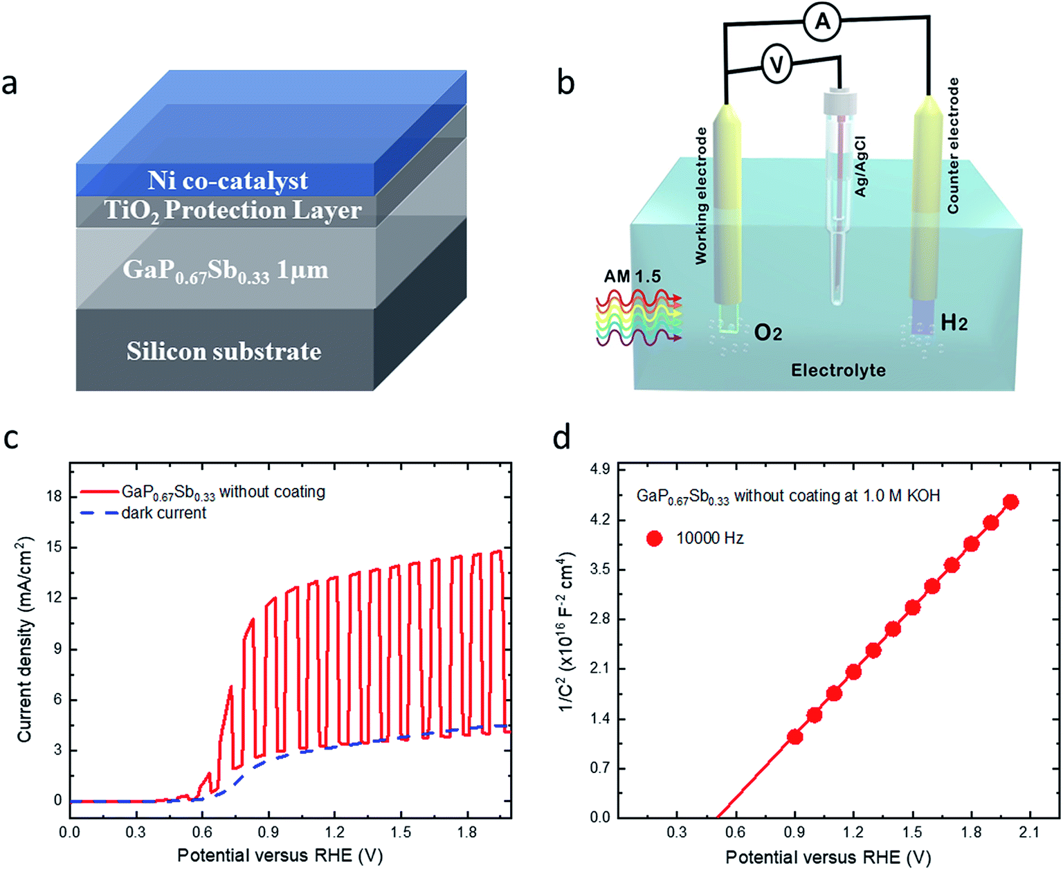 | ||
| Fig. 3 (a) Schematic diagram of the structure for the GaP0.67Sb0.33 photoanode coated with a protection layer (TiO2) and co-catalyst (Ni). (b) The experimental setup using a three-electrode system for the photoelectrochemical measurements. (c) Current density versus applied voltage (J–V) curve of GaP0.67Sb0.33 without the photoanode coating in 1.0 M KOH (pH = 14) electrolyte under simulated AM1.5 illumination versus RHE. (d) Mott–Schottky (M–S) plot as a function of the applied potential (E) for GaP0.67Sb0.33 without the photoanode coating at 10 kHz. | ||
Fig. 4a presents the current density versus potential (J–V) for GaP0.67Sb0.33 coated with TiO2 and Ni and GaP0.67Sb0.33 coated with Ni photoanodes in 1.0 M KOH (pH = 14) electrolyte under one sun illumination. As shown in Fig. 4a, the GaP0.67Sb0.33 coated with 8 nm of Ni showed an onset potential of 0.37 V and a saturated current density of 3.84 mA cm−2 at 1.23 V versus RHE. In contrast, the GaP0.67Sb0.33 coated with TiO2 (20 nm) and Ni (8 nm) showed significant improvement by increasing the photocurrent and slightly anodic shift of the onset potential relative to that of the GaP0.67Sb0.33 coated with Ni (8 nm). The onset potential shifted slightly to 0.35 V and the current density was increased to 4.82 mA cm−2 at 1.23 V versus RHE. In the absence of light, the dark current was zero compared to GaP0.67Sb0.33 without coating and GaP0.67Sb0.33 coated with Ni (8 nm) photoanodes which is attributed to the effectiveness of the protection layer formed by TiO2 with the Ni co-catalyst. Obviously, it showed the GaP0.67Sb0.33 coated with TiO2 and the Ni photoanode improved the PEC performance and photostability. On the other hand, the current density versus potential (J–V) after six potential sweeping scans is shown in Fig. 4b for three electrodes: GaP0.67Sb0.33 without coating, GaP0.67Sb0.33 coated with Ni (8 nm), and GaP0.67Sb0.33 coated with TiO2 (20 nm) and Ni (8 nm). As shown in Fig. 4b, the GaP0.67Sb0.33 without coating exhibited a sharp reduction in the photocurrent due to the photocorrosion during water oxidation which is consistent with the stability of the electrode in the next discussion. In contrast, the GaP0.67Sb0.33 coated with Ni and GaP0.67Sb0.33 coated with TiO2 and Ni showed no change in the photocurrent density versus potential (J–V) behaviour under the same conditions which suggests that there is good protection of the TiO2 layer and high activity of the Ni catalyst.31,32 Moreover, the photocurrent produced by the Si wafer photoanode is negligible in the absence of the GaP0.67Sb0.33 absorber (see Fig. S6, ESI†).
 | ||
| Fig. 4 Current density versus applied voltage (J–V) curve of GaP0.67Sb0.33 coated with Ni 8 nm and GaP0.67Sb0.33 coated with TiO2 20 nm and Ni 8 nm photoanodes in 1.0 M KOH electrolyte under simulated AM1.5 illumination versus RHE. (b) Current density versus applied voltage (J–V) curve (scan number 6) for the GaP0.67Sb0.33 photoanodes from (a). (c) Incident photon-to-current conversion efficiency (IPCE) of the GaP0.67Sb0.33 without coating, GaP0.67Sb0.33 coated with Ni 8 nm, and GaP0.67Sb0.33 coated with TiO2 20 nm and Ni 8 nm in 1.0 M KOH electrolyte at 1.23 V versus RHE and the optical absorption spectrum (for GaP0.67Sb0.33) that shows a bandgap absorption edge at 1.65 eV, (see Fig. S3, ESI†). (d) Photocurrent density versus time (J–t) characteristics for GaP0.67Sb0.33 without coating and GaP0.67Sb0.33 coated with Ni 8 nm photoanodes in 1.0 KOH (pH = 14) aqueous solution under one sun illumination. | ||
The incident photon-to-current conversion efficiency (IPCE) as a function of wavelength for the GaP0.67Sb0.33 photoanodes was further investigated at an applied bias of 1.23 V versus RHE in 1.0 M KOH electrolyte (pH = 14). As shown in Fig. 4c, the narrow bandgap of the GaP0.67Sb0.33 photoanode shows an enhanced photoresponse over the visible light range from 400 nm to 700 nm, which leads to high photocurrent density. This observation is consistent with the measured optical absorption coefficient of GaP0.67Sb0.33 in Fig. 4c and shows the benefit of the incorporation of Sb. For the GaP0.67Sb0.33 without the photoanode coating, the maximum IPCE was 58.5% at 400 nm which decreases rapidly to 18.6% at 550 nm. The poor PEC performance is attributed the oxidation/corrosion of the electrode, which is in agreement with the significantly reduced photocurrent as shown in the sixth measurement of the linear scanning voltammetry (Fig. 4b). As compared with a reference GaP photoanode, the maximum IPCE value for the GaP photoanode (see Fig. S7 in the ESI†) was ∼53.2% at 400 nm which decreases towards longer wavelengths (>550 nm). This is due to the large and indirect band gap of GaP (2.26 eV).12 By depositing 8 nm Ni as a co-catalyst, significant improvement was noticed. A maximum of 63% IPCE was achieved for the GaP0.67Sb0.33 electrode coated with 8 nm Ni at 400 nm and it gradually decreases to 53.4% at 550 nm. The IPCE of the GaP0.67Sb0.33 photoanode coated with Ni (8 nm) over the visible light region from 400 nm to 650 nm is as high as 51.16% due to a highly active oxygen evolution catalyst.33–35 In contrast, the GaP0.67Sb0.33 photoanode coated with TiO2 (20 nm) and Ni (8 nm) reached a high IPCE of 76.4% at 400 nm and 67.1% between 400 nm and 650 nm, which indicates efficient and fast charge transfer to the semiconductor/electrolyte interface. Beyond 700 nm, the IPCE falls and tends to zero around 750 nm in agreement with the energy bandgap (1.65 eV) deduced from the measured GaP0.67Sb0.33 absorption spectrum. The stability of III–V semiconductors is the critical challenge in aqueous solution.36 To assess the stability of the GaP0.67Sb0.33 photoanodes, the photocurrent density versus the time (J–t) characteristics of electrodes were investigated at a constant potential of 1 V versus RHE in a corrosive solution of 1.0 M KOH (pH = 14) as shown in Fig. 4d and 5a. The photocurrent of GaP0.67Sb0.33 without coating significantly decreased which is attributed to photocorrosion. However, after the modification of the GaP0.67Sb0.33 surface by deposition (8 nm) of Ni as a co-catalyst which is denoted as GaP0.67Sb0.33 coated with Ni (8 nm), the photocurrent remained constant for around 1.30 h with little decay in the current density and decreased sharply after that. Clearly, depositing Ni onto the surface of the GaP0.67Sb0.33 photoanode (GaP0.67Sb0.33 coated with Ni 8 nm) reduced the photocorrosion of the electrode. In contrast, using the corrosion resistant TiO2 (20 nm) layer and Ni co-catalyst (8 nm) gave drastic improvement in the stability of the electrode (GaP0.67Sb0.33 coated with TiO2 (20 nm) and Ni (8 nm)) as shown in Fig. 5a. The photocurrent of GaP0.67Sb0.33 coated with TiO2 (20 nm) and Ni (8 nm) remained stable for 5 h without degradation whereas the GaP0.67Sb0.33 without the protective TiO2 layer failed within 1.30 h. These results are attributed to the well-known corrosion resistance of TiO2 in combination with the highly active Ni catalyst, which is consistent with previous reports.37
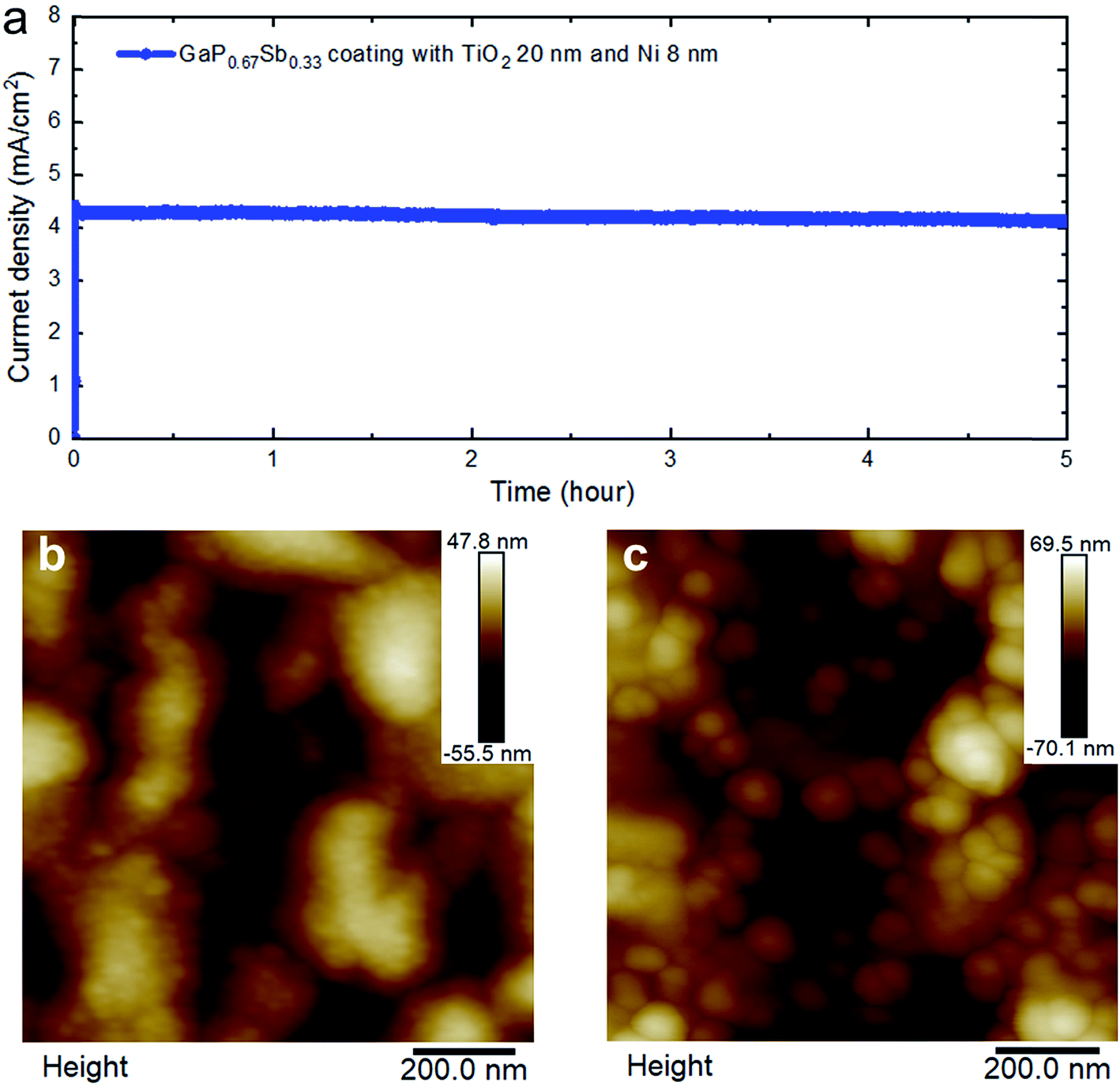 | ||
| Fig. 5 (a) Photocurrent density versus time (J–t) for GaP0.67Sb0.33 coated with TiO2 20 nm and Ni 8 nm photoanodes in 1.0 KOH (pH = 14) aqueous solution under one sun illumination. (b) Atomic force microscopy image morphology before the PEC test for the GaP0.67Sb0.33 coated with TiO2 20 nm and Ni 8 nm photoanodes. (c) AFM image morphology after five hours of PEC testing for the GaP0.67Sb0.33 coated with TiO2 20 nm and Ni 8 nm photoanodes (see Fig. S10 ESI†). | ||
To further investigate the morphology of GaP0.67Sb0.33 coated with TiO2 and the Ni photoanode before and after the 5 h stability test in 1.0 M KOH (pH = 14) electrolyte, we studied the surface of the electrode by atomic force microscopy (AFM) as shown in Fig. 5b and c. Growth of GaP0.67Sb0.33 directly on a Si substrate is challenging due to a large lattice mismatch between the two materials which causes strain to build up in the GaP0.67Sb0.33 layer. As the strain is released, dislocations form within the crystal leading to creation of defects and high surface roughness. The atomic force microscopy (AFM) image of the GaP0.67Sb0.33 surface without coating (as grown by MBE) is shown in Fig. 5b and Fig. S8 (ESI†). The RMS (root-mean-square) roughness of this surface has been calculated at 13.3 nm. After deposition of TiO2 by ALD and the Ni catalyst by thermal evaporation, the surface morphology, as shown in Fig. S9 ESI,† remains comparable to the GaP0.67Sb0.33 without coating as grown by MBE with a slight increase of the RMS surface roughness to 15.3 nm. In contrast, the morphology of the surface of GaP0.67Sb0.33 coated with TiO2 and Ni after 5 h of stability tests was changed slightly as the sharp features smooth out as shown in Fig. 5c and in S10 ESI.† However, the overall RMS roughness increases to 20.6 nm which could be attributed to the etching of the photoanode surface due to the corrosive high pH solution. From these observations, it can be inferred that the quality of the as-grown GaP0.67Sb0.33 semiconductor has the most impact on the surface roughness of the final sample (GaP0.67Sb0.33 coated with TiO2 and Ni).
Conclusion
In conclusion, we have demonstrated a direct bandgap GaP0.67Sb0.33 photoanode which offers a high absorption coefficient and substantial solar spectrum coverage. The GaP0.67Sb0.33 alloy was epitaxially grown on silicon substrates, which are potentially cost-effective for water oxidation compared to their III–V thin film counterparts. Additionally, the reduction of photoelectrode complexity and hence cost by using a single semiconductor absorber provides an alternative to expensive technologies, e.g. multijunction PEC cells. The growth of 1.65 eV GaP0.67Sb0.33 directly on 1.1 eV Si offers new opportunities for the economic fabrication of the ideal tandem PEC device. Under one sun simulated solar light irradiation, the GaP0.67Sb0.33 photoanode shows a high photocurrent density of 4.82 mA cm−2 at 1.23 V and onset potential of 0.35 V versus RHE in 1.0 M KOH (pH = 14) aqueous solution. Furthermore, the photoanode was stable for 5 h without any change in the photocurrent density at 1 V vs. RHE and a high IPCE of up to 67.1% through the visible range from 400 nm to 650 nm was achieved.Experimental section
MBE growth
The GaP0.67Sb0.33/Si sample was grown by Molecular Beam Epitaxy (MBE) on a HF-chemically prepared n-doped (1017 cm−3) Si(001) substrate, with a 6° miscut toward the [110] direction.36 The substrate was heated at 800 °C for 10 minutes to remove hydrogen from the surface. A 1 μm-thick GaP0.67Sb0.33 layer was then grown at 500 °C in a conventional continuous MBE growth mode, and at a growth rate of 0.24 ML s−1, with a Beam Equivalent Pressure V/III ratio of 5. It should be noted that the whole epilayer was nominally undoped, but on the other hand epitaxial strategies to annihilate antiphase boundaries38 were not used here, leading to emerging APBs. These APBs give an equivalent n-doping concentration of the epilayer of about 1018 cm.3Materials characterisation
The Scanning Transmission Electron Microscopy (STEM) high-resolution imaging and Energy Dispersive X-Spectroscopy (EDX) were obtained using a Hitachi HD2700 AC-STEM operated at 200 kV in high-angle annular dark field (HAADF) mode. The TEM sample was prepared using an FEI FIB200 FIB and thinned to electron transparency. A focused probe (∼0.1–1 nm diameter) is scanned across the sample surface, and transmitted electrons are imaged. Raman spectra were obtained on a Renishaw inVia micro-Raman system with 532 nm wavelength incident light.X-ray photoelectron spectroscopy (XPS) measurements were performed with a Thermo Scientific monochromated aluminium K-Alfa photoelectron spectrometer, using monochromic Al-Kα radiation (1486.7 eV). Survey scans were collected in the range of 0–1300 eV with high resolution scans for Ga 2p, Ga 3d, P 2p, Sb 3d/O 1s and C 1s. The raw data were processed using CasaXPS and calibrated to adventitious carbon at 284.5 eV.
X-ray diffraction was performed on a 4-circle Bruker D8 Diffractometer (horizontal scattering plane geometry). This diffractometer is equipped with a 1D Gobel Multi-layer Mirror placed on the linear focus window of a standard sealed tube as primary optics. A Bartels asymmetric Ge (220) monochromator was used for both line scan and reciprocal space maps. The detector is a Lynxeye™, 1 dimensional position sensitive detector (PSD) allowing a collection angle of 2.6° over 2θ. The atomic force microscopy (AFM) images here obtained using a Veeco Dimension 3100 AFM microscope, which is a high-resolution scanning probe microscope with a resolution of sub-nanometer order. The microscope has been used in the soft tapping mode with a standard non-contact probe with the cantilever tuned around 190 kHz. Atomic layer deposition of TiO2: atomic layer deposition of amorphous TiO2 (20 nm) on GaP0.67Sb0.33 grown on a Si substrate was performed using a Savannah S200 ALD system and the temperature was maintained at 150 °C. The growth rates per cycle for TiO2 were determined using a spectroscopic ellipsometer. The Ni was deposited onto the surface of the TiO2/GaP0.67Sb0.33 photoanode by thermal evaporation as a co-catalyst to accelerate the charge transfer to the semiconductor–electrolyte interface. The thermal evaporation was carried out under high vacuum in an evaporator and Ni was cleaned and loaded in the evaporator in a tungsten (W) boat, facing the electrode sample. The pressure used was 10−6 mbar then the metal was heated up by resistive heating, due to a high current going through the boat, then evaporation occurred.
Optical characterization
The optical constants of the GaP0.67Sb0.33 alloy were measured by variable angle spectroscopic ellipsometry (VASE) at room temperature in the 0.85–5 eV photon energy region. A Tauc–Lorentz model with 2 oscillators was applied to fit the ellipsometry data and extract real and imaginary parts of the refractive index in order to plot the absorption spectrum of the GaP0.67Sb0.33 alloy. The electronic structure was investigated through temperature dependent PL measurements. The samples were placed in an ARS closed-loop cryostat where the temperature can be varied between 15 K and 300 K. The excitation source is a laser diode operating at 405 nm. The laser spot size diameter on the sample is about 50 μm and the power 9.3 mW. The luminescence signal is collected using an IHR 320 spectrometer with a 300 mm−2 grating and an open-electrode Si CCD. The entrance slit of the spectrometer is set to 100 μm.Band structure modelling
The band diagram of GaP0.67Sb0.33 is calculated using an extended basis sp3d5s* tight binding Hamiltonian.18,39 This method has proved to provide a band structure description with a sub-millielectronvolt precision throughout the Brillouin zone of binary cubic III–V and II–VI27 semiconductors including quantum heterostructures40 and surfaces.41 From the tight binding parameters of GaP and GaSb binary compounds,42 a virtual crystal approximation is performed to obtain the GaP0.67Sb0.33 alloy band structure. The tight binding parameters of the virtual crystal are an arithmetic mean of the constituent materials weighted to their concentration27 except for the diagonal matrix elements related to the atomic energies of anion “s-type” and ‘p-type” states. For these states, bowing parameters are introduced to model the strong bowing of the Γ bandgap of 2.7 eV.43 With a bowing parameter equal to 9.0 eV for the s-state and equal to 2.8 eV for the p-state, the experimental bandgap for GaP0.67Sb0.33 is nicely reproduced.Device fabrication
Before the PEC experiments, the GaP0.67Sb0.33 photoanode grown on a Si substrate was fabricated by applying an indium-gallium eutectic (Aldrich) to the back of the Si wafer. Also, the single n-GaP wafer has a dopant density of ∼1 × 1018 cm3 and was fabricated as a reference photoanode. All the samples were attached by a copper wire using silver paste and covered by insulating epoxy.Photoelectrochemical measurements
The photoelectrochemical tests were performed in 1.0 M KOH (pH = 14) electrolyte using a standard three-electrode configuration, under one sun simulated solar light irradiation. The measured potentials vs. the Ag/AgCl reference electrode were converted to the standard RHE potential using the following equation:where VAg/AgCl is the experimentally measured potential with regard to the Ag/AgCl electrode, and

 is the standard potential of Ag/AgCl at 25 °C (0.1976 V vs. RHE).
IPCE measurements were carried out using the same three-electrode configuration under monochromatic light using a set of filters. The device was biased at 1.23 V versus RHE. The IPCE can be computed by using the following equation.

where the q is the electron charge (1.602 × 10⁻¹⁹ C), ε is the relative dielectric constant of GaPSb, ε0 is the vacuum permittivity (8.85 × 10⁻¹² F m−1), k is the Boltzmann constant (1.38 × 10⁻²³ J K−1) and T is the absolute temperature. EFB is the flat band. Ndopant is the free carrier density. A is the area of the electrode. E is the applied potential.

Competing financial interests
The authors declare no competing financial interests.Author contributions
M. A., C. C., and J. W. conceived the idea. M. A. performed the PEC experiments and analysed the data. S.S. performed the XPS experiment and analysed the data. L. C., R. P., Y. L., C. L. and C. C. did the optical characterization and analysis. M. A. and J. W. carried out the STEM experiment and EDX mapping. P. J. performed AFM and related analysis. A. L. and L. C. did the X-ray diffraction experiments and analysis. A. L., C. C., and L. C. N. B. contributed to structural analysis. C. C. and N. B. designed and fabricated the samples. S. B.-R. and J.-M. J. did the band structure calculations. M. A., C. C., and J. W. wrote and finalized the manuscript. I. P. P supervised M. A. All authors reviewed and commented on the manuscript.Conflicts of interest
There are no conflicts to declare.Acknowledgements
This research was supported by the French National Research Agency ANTIPODE Project (Grant no. 14-CE26-0014-01), Région Bretagne, the UK Engineering and Physical Sciences Research Council (Grant no. EP/P006973/1), and the King Abdulaziz City for Science and Technology (KACST), Riyadh, Saudi Arabia. The authors thank Prof. S. Loualiche and Pr. A. Le Corre for having shared their experience about the growth and optical properties of GaPSb alloys. Prof. M. Henini is acknowledged for having proposed the collaboration. T. Rohel and R. Bernard are also acknowledged for technical assistance during sample fabrication. V. Demange from Sciences Chimiques de Rennes is also acknowledged for access to the XRD goniometer. Mahdi Alqahtani gratefully acknowledges support and scholarship from the King Abdulaziz City for Science and Technology, Riyadh, Saudi Arabia.References
- Y. Tachibana, L. Vayssieres and J. R. Durrant, Nat. Photonics, 2012, 6, 511–518 CrossRef CAS.
- M. G. Walter, E. L. Warren, J. R. McKone, S. W. Boettcher, Q. Mi, E. A. Santori and N. S. Lewis, Chem. Rev., 2010, 110, 6446–6473 CrossRef CAS PubMed.
- A. J. Bard, Science, 1980, 207, 139–144 CrossRef CAS PubMed.
- S. Licht, B. Wang, S. Mukerji, T. Soga, M. Umeno and H. Tributsch, J. Phys. Chem. B, 2000, 104, 8920–8924 CrossRef CAS.
- O. Khaselev, Science, 1998, 280, 425–427 CrossRef CAS PubMed.
- M. M. May, H. J. Lewerenz, D. Lackner, F. Dimroth and T. Hannappel, Nat. Commun., 2015, 6, 8286 CrossRef CAS PubMed.
- A. Fujishima and K. Honda, Nature, 1972, 238, 37–38 CrossRef CAS PubMed.
- K. Iwashina and A. Kudo, J. Am. Chem. Soc., 2011, 133, 13272–13275 CrossRef CAS PubMed.
- A. Martinez-Garcia, H. B. Russell, W. Paxton, S. Ravipati, S. Calero-Barney, M. Menon, E. Richter, J. Young, T. Deutsch and M. K. Sunkara, Adv. Energy Mater., 2018, 8, 1703247 CrossRef.
- J. R. Bolton, S. J. Strickler and J. S. Connolly, Nature, 1985, 316, 495–500 CrossRef CAS.
- Y. W. Chen, J. D. Prange, S. Duhnen, Y. Park, M. Gunji, C. E. Chidsey and P. C. McIntyre, Nat. Mater., 2011, 10, 539–544 CrossRef CAS PubMed.
- S. Hu, M. R. Shaner, J. A. Beardslee, M. Lichterman, B. S. Brunschwig and N. S. Lewis, Science, 2014, 344, 1005–1009 CrossRef CAS PubMed.
- M. F. Lichterman, A. I. Carim, M. T. McDowell, S. Hu, H. B. Gray, B. S. Brunschwig and N. S. Lewis, Energy Environ. Sci., 2014, 7, 3334–3337 RSC.
- D. Bae, B. Seger, P. C. Vesborg, O. Hansen and I. Chorkendorff, Chem. Soc. Rev., 2017, 46(7), 1933–1954 RSC.
- Y. Ping Wang, J. Stodolna, M. Bahri, J. Kuyyalil, T. Nguyen Thanh, S. Almosni, R. Bernard, R. Tremblay, M. Da Silva, A. Létoublon, T. Rohel, K. Tavernier, L. Largeau, G. Patriarche, A. Le Corre, A. Ponchet, C. Magen, C. Cornet and O. Durand, Appl. Phys. Lett., 2015, 107, 191603 CrossRef.
- I. Lucci, S. Charbonnier, L. Pedesseau, M. Vallet, L. Cerutti and J. B. Rodriguez, et al. , Phys. Rev. Mater., 2018, 2(6), 060401 CrossRef CAS.
- H. B. Russell, A. N. Andriotis, M. Menon, J. B. Jasinski, A. Martinez-Garcia and M. K. Sunkara, Sci. Rep., 2016, 6, 20822 CrossRef CAS PubMed.
- I. Lucci, S. Charbonnier, M. Vallet, P. Turban, Y. Léger, T. Rohel, N. Bertru, A. Létoublon, J.-B. Rodriguez, L. Cerutti, E. Tournié, A. Ponchet, G. Patriarche, L. Pedesseau and C. Cornet, Adv. Funct. Mater., 2018, 28, 1801585 CrossRef.
- M. Feifel, J. Ohlmann, J. Benick, M. Hermle, J. Belz, A. Beyer, K. Volz, T. Hannappel, A. W. Bett, D. Lackner and F. Dimroth, IEEE Journal of Photovoltaics, 2018, 8, 1590–1595 Search PubMed.
- M. Feifel, J. Ohlmann, J. Benick, T. Rachow, S. Janz, M. Hermle, F. Dimroth, J. Belz, A. Beyer, K. Volz and D. Lackner, IEEE Journal of Photovoltaics, 2017, 7, 502–507 Search PubMed.
- E. Tea, J. Vidal, L. Pedesseau, C. Cornet, J. M. Jancu, J. Even, S. Laribi, J. F. Guillemoles and O. Durand, J. Appl. Phys., 2014, 115, 063502 CrossRef.
- C. Cornet, M. Da Silva, C. Levallois and O. Durand, in Molecular Beam Epitaxy, ed. M. Henini, Elsevier, 2nd edn, 2018, ch. 31, pp. 637–648, DOI:10.1016/b978-0-12-812136-8.00030-x.
- T. Nguyen Thanh, C. Robert, W. Guo, A. Létoublon, C. Cornet, G. Elias, A. Ponchet, T. Rohel, N. Bertru, A. Balocchi, O. Durand, J. S. Micha, M. Perrin, S. Loualiche, X. Marie and A. Le Corre, J. Appl. Phys., 2012, 112, 053521 CrossRef.
- Y. Qiu, M. Li, G. Liu, B. Zhang, Y. Wang and L. Zhao, J. Cryst. Growth, 2007, 308, 325–329 CrossRef CAS.
- Y. T. Cherng, M. J. Jou, H. R. Jen and G. B. Stringfellow, J. Appl. Phys., 1988, 63, 5444–5446 CrossRef CAS.
- Y. T. Cherng, D. H. Jaw, M. J. Jou and G. B. Stringfellow, J. Appl. Phys., 1989, 65, 3285–3288 CrossRef CAS.
- J.-M. Jancu, R. Scholz, F. Beltram and F. Bassani, Phys. Rev. B, 1998, 57, 6493–6507 CrossRef CAS.
- S. Loualiche, A. Le Corre, S. Salaun, J. Caulet, B. Lambert, M. Gauneau, D. Lecrosnier and B. Deveaud, Appl. Phys. Lett., 1991, 59, 423–424 CrossRef CAS.
- C. G. van de Walle and J. Neugebauer, Nature, 2003, 423, 626–628 CrossRef CAS PubMed.
- N. Serpone and E. Pelizzetti, Photocatalysis: fundamentals and applications, Wiley, New York, 1989 Search PubMed.
- C. Robert, A. Bondi, T. N. Thanh, J. Even, C. Cornet, O. Durand, J. P. Burin, J. M. Jancu, W. Guo, A. Létoublon, H. Folliot, S. Boyer-Richard, M. Perrin, N. Chevalier, O. Dehaese, K. Tavernier, S. Loualiche and A. Le Corre, Appl. Phys. Lett., 2011, 98, 251110 CrossRef.
- C. Robert, C. Cornet, P. Turban, T. Nguyen Thanh, M. O. Nestoklon and J. Even, et al. , Phys. Rev. B: Condens. Matter Mater. Phys., 2012, 86(20), 205316 CrossRef.
- A. Standing, S. Assali, L. Gao, M. A. Verheijen, D. van Dam, Y. Cui, P. H. Notten, J. E. Haverkort and E. P. Bakkers, Nat. Commun., 2015, 6, 7824 CrossRef CAS PubMed.
- N. C. Strandwitz, D. B. Turner-Evans, A. C. Tamboli, C. T. Chen, H. A. Atwater and N. S. Lewis, Adv. Energy Mater., 2012, 2, 1109–1116 CrossRef CAS.
- A. Kargar, S. Sukrittanon, C. Zhou, Y. G. Ro, X. Pan, S. A. Dayeh, C. W. Tu and S. Jin, Small, 2017, 13, 1603574 CrossRef.
- S. Hu, M. R. Shaner, J. A. Beardslee, M. Lichterman, B. S. Brunschwig and N. S. Lewis, Science, 2014, 344, 1005–1009 CrossRef CAS PubMed.
- J. R. McKone, N. S. Lewis and H. B. Gray, Chem. Mater., 2013, 26, 407–414 CrossRef.
- T. Quinci, J. Kuyyalil, T. N. Thanh, Y. P. Wang, S. Almosni, A. Létoublon, T. Rohel, K. Tavernier, N. Chevalier, O. Dehaese, N. Boudet, J. F. Bérar, S. Loualiche, J. Even, N. Bertru, A. L. Corre, O. Durand and C. Cornet, J. Cryst. Growth, 2013, 380, 157–162 CrossRef CAS.
- P. Guilleme, M. Vallet, J. Stodolna, A. Ponchet, C. Cornet, A. Letoublon, P. Feron, O. Durand, Y. Leger and Y. Dumeige, Opt. Express, 2016, 24, 14608–14617 CrossRef CAS PubMed.
- S. Boyer-Richard, C. Robert, L. Gerard, J. P. Richters, R. Andre, J. Bleuse, H. Mariette, J. Even and J. M. Jancu, Nanoscale Res. Lett., 2012, 7, 543 CrossRef PubMed.
- R. Scholz, J. M. Jancu, F. Beltram and F. Bassani, Phys. Status Solidi B, 2000, 217, 449–460 CrossRef CAS.
- F. Sacconi, A. Di Carlo, P. Lugli, M. Stadele and J. M. Jancu, IEEE Trans. Electron Devices, 2004, 51, 741–748 CrossRef CAS.
- F. Raouafi, R. Samti, R. Benchamekh, R. Heyd, S. Boyer-Richard, P. Voisin and J. M. Jancu, Solid State Commun., 2016, 236, 7–11 CrossRef CAS.
Footnote |
| † Electronic supplementary information (ESI) available. See DOI: 10.1039/c9se00113a |
| This journal is © The Royal Society of Chemistry 2019 |