
 Open Access Article
 This Open Access Article is licensed under a Creative Commons Attribution-Non Commercial 3.0 Unported Licence
Activating the surface and bulk of hematite photoanodes to improve solar water splitting†
Hemin
Zhang
 a,
Jong Hyun
Park
b,
Woo Jin
Byun
a,
Myoung Hoon
Song
b and
Jae Sung
Lee
*a
a,
Jong Hyun
Park
b,
Woo Jin
Byun
a,
Myoung Hoon
Song
b and
Jae Sung
Lee
*a
aSchool of Energy and Chemical Engineering, Ulsan National Institute of Science and Technology (UNIST), 50 UNIST-gil, Ulsan 44919, Republic of Korea. E-mail: jlee1234@unist.ac.kr
bPerovtronics Research Center, Ulsan National Institute of Science and Technology (UNIST), UNIST-gil 50, Ulsan, 44919, Republic of Korea
First published on 1st October 2019
Abstract
A simple electrochemical activation treatment is proposed to improve effectively the photoelectrochemical performance of Nb,Sn co-doped hematite nanorods. The activation process involves an initial thrice cathodic scanning (reduction) and a subsequent thrice anodic scanning (oxidation), which modifies both the surface and bulk properties of the Nb,Sn:Fe2O3 photoanode. First, it selectively removes the surface components to different extents endowing the hematite surface with fewer defects and richer Nb–O and Sn–O bonds and thus passivates the surface trap states. The surface passivation effect also enhances the photoelectrochemical stability of the photoanode. Finally, more Fe2+ ions or oxygen vacancies are generated in the bulk of hematite to enhance its conductivity. As a result, the photocurrent density is increased by 62.3% from 1.88 to 3.05 mA cm−2 at 1.23 VRHE, the photocurrent onset potential shifts cathodically by ∼70 mV, and photoelectrochemical stability improves remarkably relative to the pristine photoanode under simulated sunlight (100 mW cm−2).
1. Introduction
Photoelectrochemical (PEC) water splitting is a promising technology to convert solar energy directly into a storable hydrogen fuel using semiconductor photoelectrodes that can absorb sunlight and generate electron–hole pairs.1 For practical applications, the photoelectrodes are required to have a high solar-to-hydrogen conversion efficiency (ηSTH) greater than 10%, stability in an aqueous solution without photocorrosion, and low cost. Hematite is considered an ideal candidate photoanode material for PEC water splitting because of its natural abundance, good stability, an ideal bandgap of 2.1 eV for ample visible light absorption, and a suitable band position to drive water oxidation. However, it has some critical drawbacks that should be overcome to obtain a high ηSTH, including a short hole diffusion length, poor conductivity, and a large overpotential for water oxidation.2,3A multitude of strategies have been developed to improve the PEC performance of hematite by addressing these shortcomings. Making a nanostructure (especially one-dimensional, small-diameter nanorods) can reduce the electron–hole recombination by shortening the actual diffusion distance of charge carriers. Elemental doping and/or creating oxygen vacancies (VO) are effective to improve its conductivity by enhancing the charge carrier density.4,5 Surface engineering can effectively overcome its large overpotential and low photocurrent density problems by removing the surface states through introducing a passivation layer and loading a co-catalyst.6–8
In addition to these traditional modification strategies, some post-synthetic treatments can also significantly improve the performance of photoanodes for PEC water splitting. For example, Zou et al. reported a surface corrosion method in acid solution to reduce the overpotential of Ti4+-doped hematite by suppressing the back reaction.9 Li et al. reported an acid treatment method to improve the photocurrent density by suppressing electron–hole recombination in Sn4+-doped hematite.10 Jang et al. reported a re-growth strategy to reduce surface disorders of NiFeOx-loaded hematite to achieve an onset voltage (Von) of 0.45 V (vs. the reversible hydrogen electrode, RHE).6 It was also reported that the PEC performance of BiVO4 was improved by ultraviolet irradiation11 and electrochemical treatments.12 Herein, we demonstrate a simple electrochemical process involving repeated reduction/oxidation to enhance the PEC performance of a Nb,Sn co-doped hematite nanorod (Nb,Sn:Fe2O3 NR) photoanode.
2. Results and discussion
2.1 Synthesis and characterization of Nb,Sn co-doped hematite nanorods
Scheme 1 shows schematics of the synthesis and electrochemical activation process of small Nb,Sn:Fe2O3 NRs synthesized on F:SnO2 (FTO) glass substrates according to our previously reported method.13,14 In brief, ultrathin FeOOH nanorods are first grown on FTO by a hydrothermal method and turned into amorphous hematite nanorods at 400 °C for 2 h. Then, a low concentration of NbCl5 solution is spin-coated and the second heating follows under the same conditions. Subsequently, hybrid microwave annealing (HMA) treatment is adopted to take advantage of its unique characteristics: (i) reaching extremely high temperature in a very short time of a few minutes, (ii) preserving original nanoscale morphology under harsh fabrication conditions, and (iii) negligible damage of FTO substrates at a high temperature. These features of HMA are highly beneficial for the fabrication of efficient photoelectrodes, which the conventional thermal annealing cannot provide. Finally, the synthesized photoelectrode is electrochemically activated through an initial thrice cathodic scanning (reduction) and a subsequent thrice anodic scanning (oxidation). As discussed below, the activation treatment modifies both the bulk and surface properties of Nb,Sn:Fe2O3 NRs, leading to markedly enhanced PEC performance.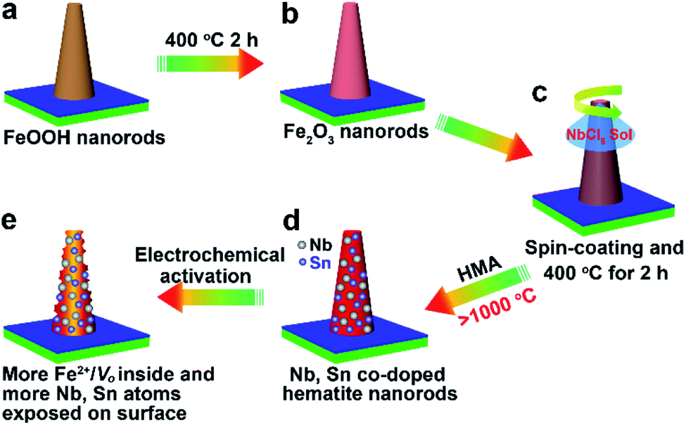 | ||
| Scheme 1 Synthesis and electrochemical activation process of a Nb,Sn:Fe2O3 NR photoanode. | ||
Our previous reports demonstrated that all the spin-coated Nb/Ta atoms were incorporated into the hematite lattice by the highly effective HMA.13,14 Simultaneously, Sn atoms would also diffuse into the hematite lattice from the bottom FTO substrate to complete the fabrication of Nb,Sn co-doped Fe2O3 nanorods. Electron energy loss spectroscopy (EELS) mapping (Fig. 1a–e) gives the spatial distribution of elements in hematite NRs, indicating that Fe, O and Nb are uniformly distributed in the whole nanorod and Sn has a little gradient from bottom (FTO source) to top. Furthermore, a high-angle annular dark-field scanning transmission electron microscopy (HAADF-STEM) image (Fig. 1f) shows many bright atoms (circled), which must be the external doping atoms of Nb and Sn. Note that there are no attached nanoparticles on the nanorod surface, which demonstrates that all the spin-coated Nb atoms have been diffused into hematite lattices. Besides, the corresponding energy dispersive X-ray spectrum (EDX) shows that the concentrations of Nb and Sn in hematite NRs are 0.9 at% and 0.4 at%, respectively (Fig. S1, ESI†). The inductively coupled plasma optical emission spectrometry (ICP-OES) results demonstrate 5.5 wt% Nb (Fig. S2†), which agrees well with 0.9 at% Nb (∼5.2 wt%) by TEM-EDX. The electrochemical activation process proposed here involves a thrice cathodic linear scanning followed by another thrice anodic linear scanning (detailed information in Fig. S3†). The treatment was conducted in 1 M KOH solution in the dark using a three-electrode cell with the Nb,Sn:Fe2O3 NR photoanode, Ag/AgCl (3 M NaCl), and Pt mesh as working, reference, and counter electrodes, respectively. The simple electrochemical process involving repeated reduction and oxidation enhances the PEC performance of the photoanode by modifying both the surface and bulk properties of hematite as detailed below.
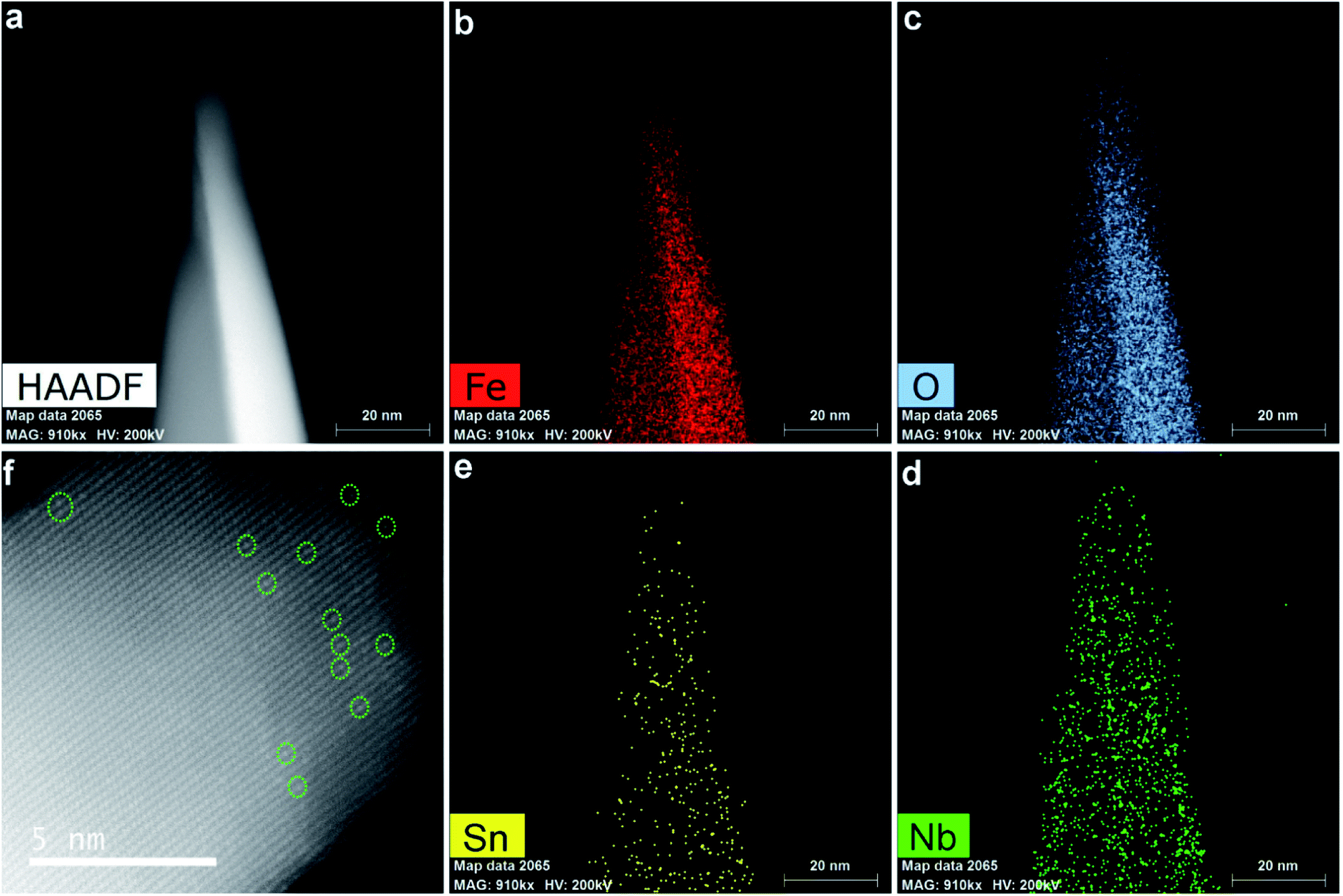 | ||
| Fig. 1 STEM (a), corresponding EDX mapping ((b–e), Fe, O, Nb and Sn, respectively) and high-resolution HAADF-STEM (f) images of the synthesized Nb,Sn co-doped hematite nanorods. | ||
Scanning electron microscope (SEM) images show no change in morphological features before (Fig. 2a) and after (Fig. 2b) the electrochemical treatment, both showing small nanorods with diameters of 20–50 nm. The activated sample also has a smooth surface similar to the pristine sample, and comparable surface areas measured using the adsorbed methylene blue dye (Fig. S4†). The X-ray diffraction (XRD) pattern after the activation treatment does not show any decreased peak intensities or shifted peak positions (Fig. 2c). Besides, Nb,Sn:Fe2O3 shows a little smaller diameter (increased full width at half maximum) and positive peak shifts relative to only Sn-doped hematite (Fig. S5†), indicating that Nb atoms from the surface coating are effectively doped into the hematite lattice while preserving the original nanostructure. Moreover, absorption spectra before and after the treatment are nearly superimposable (Fig. 2d), thus ruling out any change in light harvesting capability by the activation process. High resolution transmission electron microscopy (HRTEM) images show that there are many defects (including dangling bonds, amorphous state Fe2O3, interstitial and vacancy defects) found on the surface of the hematite nanorod before activation (highlighted in Fig. 2e). In contrast, the surface is much cleaner after the activation (Fig. 2f), indicating that a type of etching takes place during the process. Both samples show well-defined HRTEM lattice fringes denoting preferential orientation of [012], indicating that the electrochemical activation does not change the high crystallinity induced by HMA, which is consistent with the XRD results.
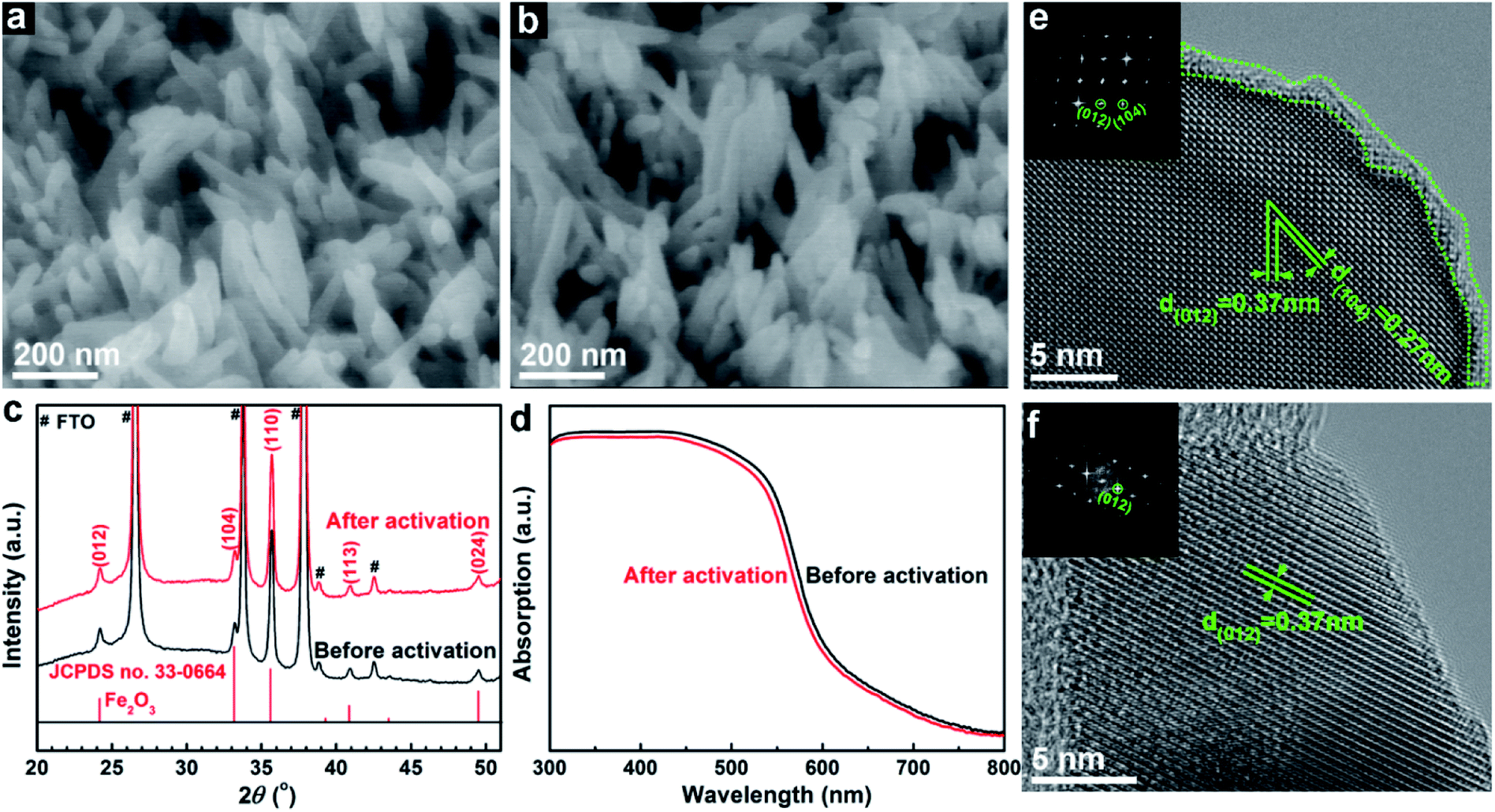 | ||
| Fig. 2 SEM images ((a), before; (b), after), XRD (c) and UV-vis spectra (d) HRTEM (e and f) of the hematite photoanode before and after the electrochemical activation treatment. Insets (e and f) show the corresponding fast Fourier transform diffraction patterns (FFTs). | ||
2.2 Effects of the activation treatment on the surface and bulk properties of hematite
Surface-sensitive X-ray photoelectron spectroscopy (XPS) was combined with Ar+ etching to investigate the depth-dependent compositions of Nb,Sn:Fe2O3 photoanodes before and after the activation treatment. It should be noted that 300 s operation in our depth profiling achieves ∼5 nm surface etching, which was estimated with a planar hematite film (synthesized by HMA) on silicon substrates. When the etching time exceeds 300 s, the intensity of the Nb 3d spectrum of the as-prepared Nb,Sn:Fe2O3 nanorod sample begins to decrease. As shown in Fig. 3a0–d0, there is almost no difference in XPS spectra of the pristine Nb,Sn:Fe2O3 NRs before and after surface etching for 300 s (except that Fe 2p and O 1s show a very limited decrease of intensity), demonstrating that the as-synthesized Nb,Sn:Fe2O3 NRs by HMA are homogeneous in composition from the surface (before etching) to bulk (after etching) of the hematite. In contrast, the activated photoanode in Fig. 3a1–d1 shows significant differences. Upon etching, the intensity of Fe 2p and O 1s spectra decreases by 41.6% and 28.3%, while that of Nb 3d and Sn 3d spectra increases by 2.8% and 1.6%, respectively, which demonstrates that the activation process selectively removes the surface components of Nb,Sn:Fe2O3 to a different extent. As shown in Fig. S6,† the varied intensity was calculated from the integrated XPS peak areas. Thus, the activation treatment selectively removes Fe from the surface, which reflects its weakest bond energy: Do298/kJ mol−1 = Fe–O (407) < Sn–O (528) < Nb–O (726).15 As a result, more Nb and Sn atoms remain on the surface than in the bulk after the treatment.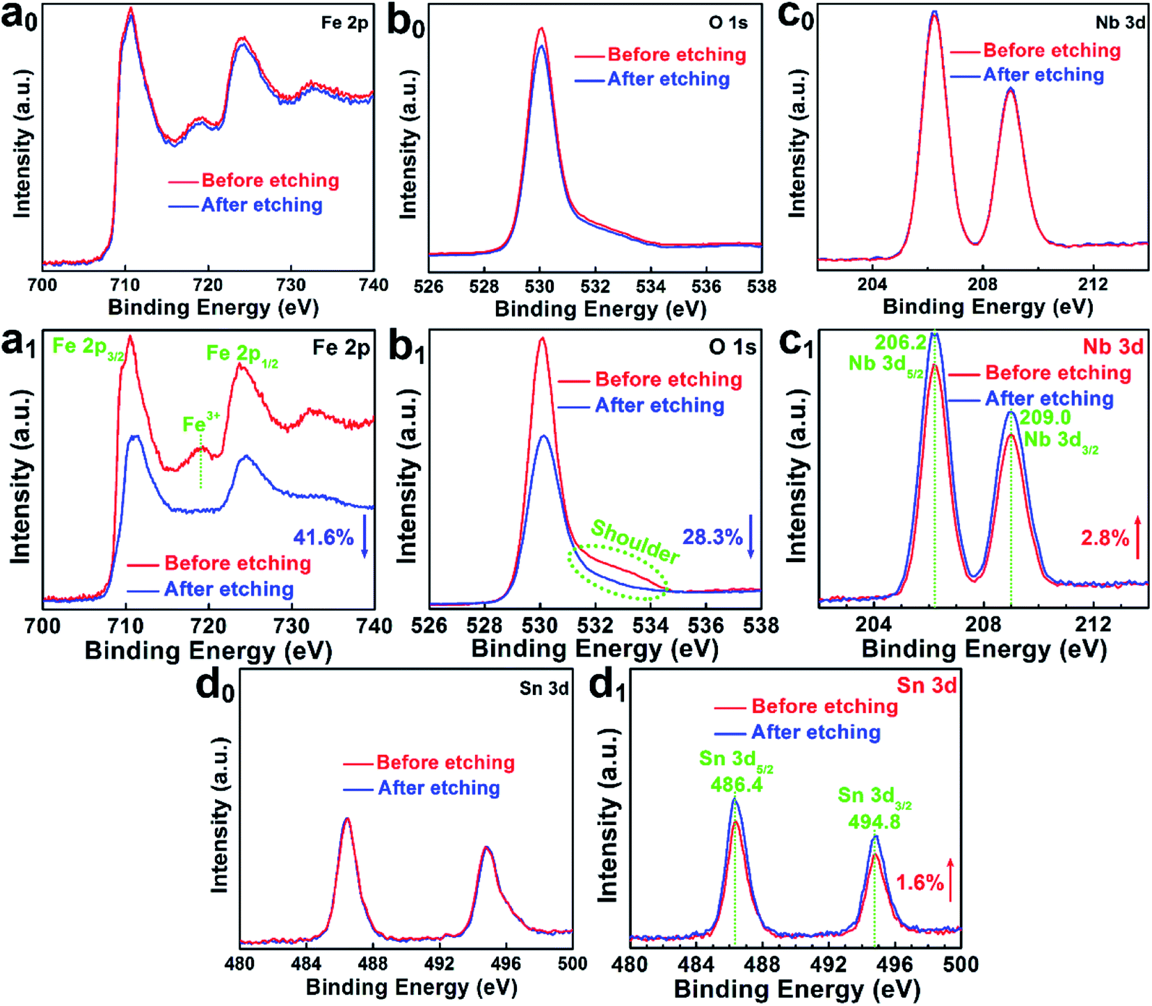 | ||
| Fig. 3 XPS spectra of the pristine and activated Nb,Sn:Fe2O3 photoanode before and after surface etching (∼5 nm), respectively. (a0 and a1) Fe 2p. (b0 and b1) O 1s. (c0 and c1) Nb 3d. (d0 and d1) Sn 3d. | ||
The electrochemical activation treatment brings another significant change in Fe 2p spectra (Fig. 3a1). Both pristine and activated Nb,Sn:Fe2O3 samples show Fe 2p3/2 (∼711.2 eV) and Fe 2p1/2 (∼724.8 eV) peaks as typical for Fe3+ in Fe2O3.16 However, the surface of the activated sample shows a satellite peak of Fe3+ at 719.3 eV, which disappears after ∼5 nm etching indicating the presence of more Fe2+ ions or VO in the bulk of activated Nb,Sn:Fe2O3 compared with the pristine sample (Fig. 3a0). In O 1s spectra (Fig. 3b1), the surface of the activated sample exhibits a notable shoulder peak (dot circled) in the range of 531.9–533.7 eV, which can be attributed to defect sites, e.g. dangling oxo or hydroxyl groups usually observed around ∼532.0 eV (ref. 17) and chemisorbed oxygen at 532.4–533.7 eV.18 This peak is not observed in the bulk after ∼5 nm etching. Fig. 3c1 displays typical peaks of Nb 3d5/2 at ∼206.2 eV and Nb 3d3/2 at ∼209.0 eV due to Nb5+, both on the surface and in the bulk. Besides, the binding energy of Nb 3d5/2 is between Nb2O5 (207.1 eV) and metallic Nb (202.4 eV), suggesting that Nb5+ ions are indeed doped into the Fe2O3 lattice.19 The Sn 3d spectra in Fig. 3d1 exhibit two peaks centred at 486.4 eV for Sn 3d5/2 and 494.8 eV for Sn 3d3/2. The binding energy of Sn 3d5/2 is between the typical values for SnO2 (486.6 eV) and metallic Sn (484.6 eV), indicating that the Sn4+ dopants are also incorporated into the hematite lattice.20 The change in the surface and bulk elemental structure before and after the electrochemical activation is schematically illustrated in Fig. S7.† Considering that the profiling depth of the pristine sample may not be deep enough due to the reduced thickness of the surface amorphous layer by activation, we extended the depth profiling time further to 400 and 500 s for the pristine sample (Fig. S8†). All the elements maintained exactly the same signals but with decreased intensities, which further demonstrates the homogeneous composition of the pristine sample from outside to inside.
2.3 Effects on photoelectrochemical water oxidation performance
After the electrochemical activation, the photocurrent density of PEC water oxidation reaches 3.05 mA cm−2 at 1.23 VRHE in 1 M KOH electrolyte under 1 sun (100 mW cm−2) irradiation, which is significantly higher (by 62.3%) than that of the pristine photoanode (1.88 mA cm−2) as shown in Fig. 4a. More significantly, the photocurrent onset potential (Von) exhibited a modest cathodic shift of ∼70 mV, which was also similar to the shift (∼50 mV) estimated by the first order derivative of the photocurrent density against the voltage21 (Fig. S9†). The modest shift of Von should be related to the extremely thin surface passivation layer (only rich Nb–O and Sn–O bonds), which might not be a continuous layer and cannot accumulate many photoexcited holes on the surface. The measured photovoltage (Fig. S10†) also shows ∼40 mV increase from 160 mV (pristine) to 200 mV (after activation), which are consistent with previously reported values.22 It should be emphasized that the results were highly reproducible, which was consistently observed for the other repeated samples (Table S1†). By comparison, the pristine sample with a lower photocurrent exhibited a tendency to show a little higher extent of improvement after the activation. In fact, the activation process causes a little decreased surface area by 2.6% (Fig. S4†) by removal of some defective/amorphous part of hematite as indicated by HRTEM images in Fig. 1 and the XPS results in Fig. 3. In addition, the corresponding dark current of the water oxidation reaction is suppressed after the activation (inset of Fig. 4a). This behaviour implies a lower electrocatalytic activity, which was also observed in previous reports on acid-treated, doped-hematite and UV light-treated BiVO4.9–11 Obviously, the reduced surface area and the lower catalytic activity would not have contributed to the improved PEC performance in any positive manner. Then how does the activation treatment enhance the PEC performance of the Nb,Sn:Fe2O3 photoanode?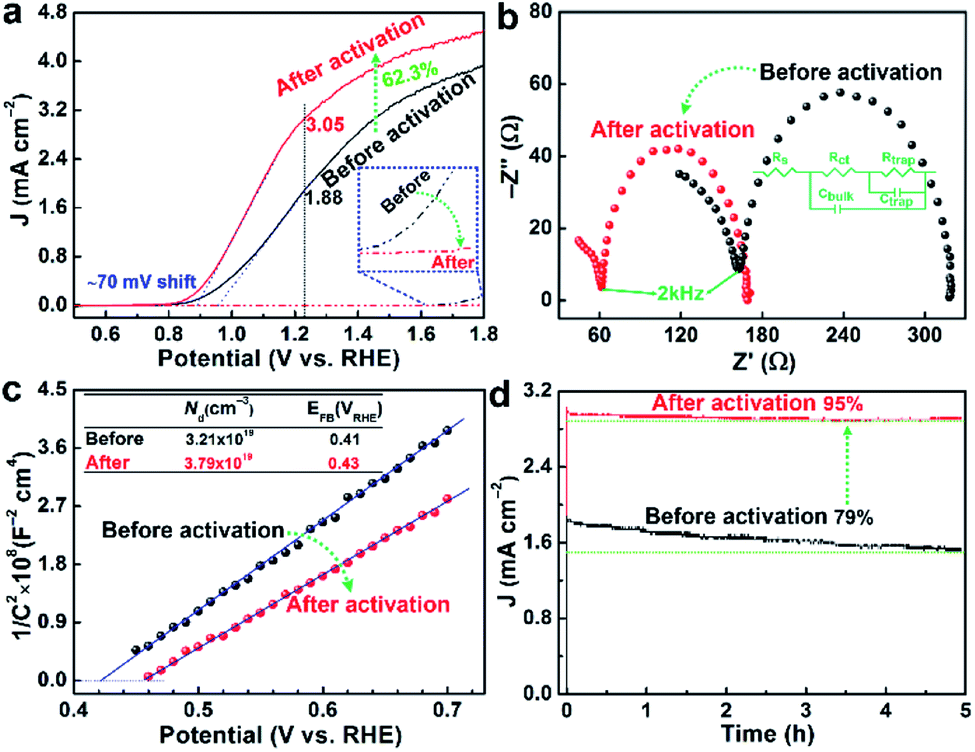 | ||
| Fig. 4 Dark current (dashed) and photocurrent (solid) densities of PEC water oxidation in 1 M KOH electrolyte under 1 sun (100 mW cm−2) irradiation (a), Nyquist plots of EIS (b), Mott–Schottky plots (c) and stability tests (d) of the Nb,Sn:Fe2O3 photoanode before and after the activation treatment. | ||
As discussed, XPS combined with etching demonstrates that the activated Nb,Sn:Fe2O3 shows more Fe2+ ions or VO in the bulk (etched surface) relative to the pristine photoanode (Fig. 3). As is well known, doping of high-valent Nb5+ and Sn4+ into the Fe2O3 lattice would enhance its n-type character by converting some Fe3+ into Fe2+ for charge compensation.23 Electrochemical reduction during cathodic scanning of the activation process produces a sub-stoichiometric metal oxide by introduction of VO,24 which is actually +2 charged and thus contributes to the n-type conductivity in the same manner as the metal doping.25 It is difficult to maintain them near the surface because of contact with the electrolyte and water oxidation reaction during the anodic scanning, but they are well preserved in the bulk. In particular the highly doped Nb,Sn:Fe2O3 NRs are favorable to preserve Fe2+ ions or VO in the bulk because their strong n-type character would make more free electrons available in the hematite lattice to suppress re-oxidation.
In order to demonstrate validity of the proposed sequential redox activation process, we tried the reverse sequence of thrice anodic scanning first followed by thrice cathodic scanning. The corresponding XPS spectra show decreased intensity of Fe 2p by only 25.2% (Fig. S11a†), which is ∼60% that of Fe 2p spectra in Fig. 3a1, indicating that the selective removal of Fe3+ ions from the surface is much less significant.
In addition, the satellite peak of Fe3+ at 719.3 eV still has a significant intensity remaining in the etched sample, indicating formation of fewer Fe2+ ions or VO in the bulk. As a result, the corresponding PEC performance of the Nb,Sn:Fe2O3 photoanode activated by the reversed sequence exhibits only 39.8% improved photocurrent and 30 mV shift of Von (Fig. S11b†). Therefore, cathodic scanning first and subsequent anodic scanning are essential for the efficient activation process, leading to significantly enhanced PEC performance, i.e. 62.3% higher photocurrent and ∼70 mV shift of Von as in Fig. 4a. Generally, the same element ions with different valences in equivalent points of a crystal lattice lead to a jumping mechanism for electronic conductivity26 as in the present case of Nb,Sn:Fe2O3 NRs.
Nyquist plots of electrochemical impedance spectroscopy (EIS) in Fig. 4b for both activated and pristine electrodes are characterized by two semicircles at high (fH, 100–2 kHz) and low (fL, 2000–0.1 Hz) frequencies. They could be fitted by a simple equivalent model of two circuits (inset), which was first discussed by Hamann and Bisquert.27,28 The loop at fH usually reflects the information of charge carriers in bulk hematite (Rct/Cbulk), while the loop at fL represents the information about the hematite/electrolyte interface (Rtrap/Ctrap). The fitting results are summarized in Table S2.† The sheet resistance of Rs (involving the electrolyte, external contact, and FTO resistances) is small and essentially constant.29 The resistance Rct is reduced by 33.4% by the activation treatment, probably by improved conductivity due to generation of more Fe2+ ions or VO in the bulk of Nb,Sn:Fe2O3 NRs. More importantly, Rtrap decreases significantly by 50.7% by selective removal of defects, unsaturated covalent bonds, and adsorbates on the surface while maintaining substantial Nb–O and Sn–O bonds. Moreover, the capacitances of Cbulk and Ctrap increase considerably after the activation.
Mott–Schottky plots were acquired from bulk capacitance values of EIS spectra, which gave the flat band potential (EFB, the intercept values on the X-axis) and the donor density (ND, inversely proportional to the slopes). In Fig. 4c, the electrochemical activation gives 18.1% increase of ND and a positive shift of EFB from 0.41 to 0.43 VRHE, which are consistent with the reported values of hematite.30 The increased ND must be related to generation of more Fe2+ ions or VO, in agreement with the above XPS/EIS results and a previous report for formation of Fe3O4 from Fe2O3 by electrochemical introduction of Fe2+ ions.31
On the surface of hematite, a range of different trap states including VO, crystal defects, and hole accumulation sites (Fe![[double bond, length as m-dash]](https://www.rsc.org/images/entities/char_e001.gif) O) are proposed to be detrimental to PEC efficiency. As demonstrated above, there exist more Nb and Sn elements on the surface of Nb,Sn:Fe2O3 NRs after the activation, which would selectively passivate such states and consequently contribute to the enhanced photocurrent density and/or cathodically shifted Von. Indeed, a very thin layer of Ta2O5 was demonstrated to have a good passivation effect on the hematite surface.32 Likewise, the mostly remaining Nb–O and Sn–O bonds on the hematite surface after activation should have a similar beneficial effect. In addition, they also contribute significantly to the stability of the photoanode because of their high bond energies. Indeed, Fig. 4d shows clearly enhanced stability after the activation treatment, maintaining 95% of initial photocurrent generation after 5 h of PEC water oxidation, whereas the pristine photoanode maintains only 79% of the initial activity. The results also confirm that the activated state remains stable and irreversible during the PEC water oxidation.
O) are proposed to be detrimental to PEC efficiency. As demonstrated above, there exist more Nb and Sn elements on the surface of Nb,Sn:Fe2O3 NRs after the activation, which would selectively passivate such states and consequently contribute to the enhanced photocurrent density and/or cathodically shifted Von. Indeed, a very thin layer of Ta2O5 was demonstrated to have a good passivation effect on the hematite surface.32 Likewise, the mostly remaining Nb–O and Sn–O bonds on the hematite surface after activation should have a similar beneficial effect. In addition, they also contribute significantly to the stability of the photoanode because of their high bond energies. Indeed, Fig. 4d shows clearly enhanced stability after the activation treatment, maintaining 95% of initial photocurrent generation after 5 h of PEC water oxidation, whereas the pristine photoanode maintains only 79% of the initial activity. The results also confirm that the activated state remains stable and irreversible during the PEC water oxidation.
Steady-state photoluminescence spectroscopy (PL) and time-resolved PL were used to monitor the charge transfer dynamics in the activated Nb,Sn:Fe2O3 photoanode. Generally, bulk Fe2O3 exhibits little PL because of serious nonradiative recombination. However, its PL is highly dependent on surface quality, especially on surface trap density.33 Therefore, PL would be enhanced when surface states are even partially eliminated by the activation process. The PL spectra of both activated and pristine Nb,Sn:Fe2O3 NRs in Fig. 5a show a weak emission-beginning peak at 575 nm (2.15 eV) and a relatively strong emission peak at 615 nm, which are consistent with previous reports of hematite.34 In addition, the bare FTO treated under the same conditions as Nb,Sn:Fe2O3 synthesis shows no PL signal in the measured range (Fig. S12†). The enhanced PL of the activated sample is strong evidence that a part of surface trap states is passivated in the electrochemical activation process by selective removal of defects and retaining more Nb–O and Sn–O bonds.
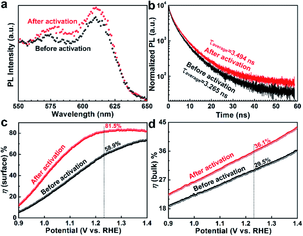 | ||
| Fig. 5 Steady state PL spectra (a), time-resolved PL spectra (b), surface charge separation efficiency, ηsurface (c), and bulk charge separation efficiency, ηbulk (d) of the Nb,Sn:Fe2O3 nanorod photoanode before and after the activation treatment. | ||
In time-resolved PL (Fig. 5b), the activated sample shows a little higher tailing relative to that of the pristine sample, indicating that the activated sample has a longer charge carrier lifetime. The measured charge carrier lifetime denotes the time that takes for electron–hole pairs to decay to 1/e by radiative recombination.35 Therefore, the longer lifetime means a slower recombination of the charge carriers. From the fitting of the PL decay kinetics, the amplitude weighted average lifetimes were τavg = 3.494 ns for the activated sample and τavg = 3.265 ns for the pristine sample (other parameters in Table S3†). In general, the short PL lifetime of hematite is attributed to the fast recombination between holes and electrons, which results from its short hole diffusion length. However, the activated sample shows 7% longer lifetime than that of the pristine sample, which must be related to the surface passivation effect by selective removal of surface trap sites and more Nb–O and Sn–O bonds retained on the surface by the activation process.
The surface (ηsurface) and bulk (ηbulk) charge separation efficiencies were determined by comparing photo-oxidation currents of water and a hole scavenger (0.5 M H2O2) in the same electrolyte (1 M KOH). The detailed procedures are shown in Fig. S13.† The ηsurface represents the fraction of holes at the interface that is successfully injected to the electrolyte to oxidize water without recombination on the semiconductor surface, while ηbulk is the fraction of holes that reach the interface of the semiconductor/electrolyte without recombination in the bulk. As in Fig. 5c, ηsurface improves from 58.9% to 81.5% at 1.23 VRHE after the electrochemical activation, indicating that the surface properties of hematite nanorods have been significantly improved by removal of surface trap sites and surface passivation by more Nb–O and Sn–O bonds retained. The ηbulk also improves from 29.5% to 36.1% at 1.23 VRHE upon the electrochemical activation (Fig. 5d), indicating that the generated Fe2+ ions or VO effectively enhances the electrical conductivity in the bulk of hematite. These results further support the aforementioned discussion on the effect of the activation treatment.
2.4 Application to other photoanodes
In order to test the general applicability of our electrochemical activation process, it was applied to two related materials. The first was Nb,Sn:Fe2O3@FeNbO4 core–shell heterojunction NRs that we studied in our previous work.13 As shown in Fig. S14,† the activation of the core–shell heterojunction shows very limited (only 6.2%) increase of photocurrent. The other repeated samples show similar behaviour (Table S4†). Because of high stability of the FeNbO4 shell and strong n-type character of the core, we cannot take advantage of the beneficial effects of selective removal of the surface components to passivate surface trap sites and introduction of VO/Fe2+ in lattices to increase the conductivity. The second test material was only Sn-doped hematite, which showed marked effects of the activation treatment. As shown in Fig. S15,† the photocurrent is improved by 44.4%, (from 1.24 to 1.79 mA cm−2 at 1.23 VRHE under 1 sun condition), which is comparable to the present Nb,Sn:Fe2O3 photoanode (62.3% increase). The other activated samples (Table S5†) also show reproducible results and the same tendency with the Nb,Sn:Fe2O3 electrode (higher extent of improvement on the poorer pristine sample). This is reasonable because the poor pristine samples (prepared under the same conditions) usually have more surface states, and most of them would be passivated by the activation. The results confirm that our activation strategy is applicable to improve the activity of hematite-based photoanodes in general, but is not very effective for hematite with a stable protective layer, for which the selective removal of the surface components is difficult.3. Conclusions
In summary, we have demonstrated a simple and effective electrochemical activation process that improves the PEC water oxidation performance of the Nb,Sn:Fe2O3 photoanode in terms of photocurrent density, onset potential, and stability. The activation process involves initial thrice cathodic scanning followed by thrice anodic scanning, which makes three main modifications of hematite. First, it selectively removes the surface components to different extents endowing the hematite surface with fewer defects and richer Nb–O and Sn–O bonds and thus passivates the surface trap states. The surface passivation effect also enhances the PEC stability of the photoanode. Finally, more Fe2+ ions or VO is generated in the bulk of hematite to enhance its conductivity. These changes in the bulk and on the surface of hematite are responsible for the greatly enhanced PEC performance by improving charge separation efficiencies both on the surface (ηsurface) and in the bulk (ηbulk). The electrochemical activation strategy proposed here could be extended to a number of other metal oxide semiconductors including WO3, TiO2, BiVO4 and ZnO for significantly improved PEC water splitting activity.4. Experimental section
4.1 Fabrication of ultrathin FeOOH nanorods on FTO substrates
Conductive FTO substrates (PECTM 8, 6–9 Ω, Pilkington) of 25 × 50 mm2 were cleaned by ultrasonication for 30 min in detergent, ethanol, and acetone, respectively. The FTO surface becomes sufficiently hydrophilic by this cleaning process. The FeOOH nanorods grow on FTO at 100 °C for 2 h using 100 mL of an aqueous solution containing 4.0 g FeCl3·6H2O (Sigma Aldrich, ≥99%), 200 μL HNO3 (Sigma Aldrich, 70%) and 8.4 g NaNO3 (Sigma Aldrich, ≥99%). The obtained yellow-colored FeOOH nanorod film after cooling down was rinsed with abundant deionized water.4.2 Hybrid microwave annealing (HMA)
The prepared samples (12.5 × 12.5 mm2) were put on graphite powder (60 mL graphite as a susceptor) in a Pyrex beaker (100 mL) and treated in a microwave oven (2.45 GHz, 1000 W) for 2 min (100% power).4.3 Physical characterization
The morphology of the samples was acquired using a field-emission scanning electron microscope (FESEM-S4800, HITACHI). High-angle annular dark-field scanning transmission electron microscopy (HAADF-STEM) images and corresponding electron energy loss spectroscopy (EELS) mapping were taken using a FEI Titan3 G2 60-300 microscope equipped with a double-sided Cs corrector operating at 200 kV. High resolution TEM (HRTEM) images in bright field were obtained using a Cs-corrected high-resolution transmission electron microscope (JEOL, JEM-2100F, 200 kV). X-ray diffraction (XRD) spectra were acquired using a PW3040/60 X'per PRO, PANalytical, using Cu-Kα (λ = 1.54056 Å) radiation, an accelerating voltage of 40 kV and a current of 30 mA. Ultraviolet-visible absorbance was obtained using a UV-vis spectrometer (UV-2401PC, Shimadzu). X-ray photoelectron spectroscopy (XPS) was carried out on a Thermo-Fisher machine (XPS, ESCALAB 250XI) using an Al Kα source. Inductively coupled plasma optical emission spectrometry (ICP-OES) was obtained on a Varian machine (700-ES). Steady state photoluminescence (PL) measurements were conducted on a spectrofluorometer (FLS920) with an excitation wavelength of 450 nm using a 450 W xenon lamp excitation source and a photomultiplier tube detector. Time-resolved PL spectra were measured using a time-correlated single-photon counting (TCSPC) setup (FluoTime 300). The excitation source was a 450 nm continuous-wave and pulsed diode laser head (LDH-D-C-450) coupled with a laser diode driver (PDL 820) with a pulse width of <70 ps and a repetition rate of 196 kHz to 40 MHz. Each exponential decay curve was deconvoluted using the associated fitting software (FluoFit) to calculate the time constant associated with each curve.4.4 (Photo)electrochemical measurements
All (photo)electrochemical measurements were conducted on a potentiostat (IviumStat, Ivium Technologies) in a three electrode system using a hematite photoanode, Ag/AgCl (3 M NaCl), and Pt mesh as working, reference, and counter electrodes, respectively, in 1 M KOH electrolyte under 1-sun condition (100 mW cm−2) using a solar simulator (91160, Oriel) with an AM 1.5 G filter. Note that the exposed surface area of all the prepared photoanodes was 1 cm2 and the electrolyte was slowly stirred during the measurements. All the potentials vs. the Ag/AgCl reference electrode were converted to the potentials vs. the reversible hydrogen electrode (RHE) according to the Nernst equation: ERHE = EAg/AgCl + 0.059 pH + EoAg/AgCl (EoAg/AgCl = 0.1976 at 25 °C). The potential was swept in the range of 0.5–1.8 VRHE with a scanning rate of 20 mV s−1. Electrochemical impedance spectroscopy (EIS) was carried out at 1.23 VRHE under simulated 1-sun condition with a frequency range of 0.1 Hz to 100 kHz and the data were fitted by Z-view software. Mott–Schottky plots were obtained by sweeping a 0.1–1.0 VRHE range with an AC frequency of 1000 Hz under dark conditions. The charge carrier density, ND, can be extracted and is inversely proportional to the slope as shown in eqn (1):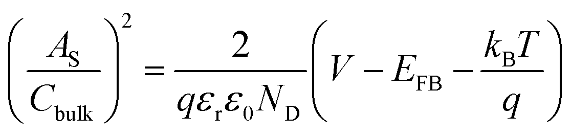 | (1) |
 being the surface area-corrected space charge capacitance, V the applied potential, EFB the flat band of the electrode, kB = 1.38 × 10⁻²³ J K−1, T = 298 K, q = 1.602 × 10⁻¹⁹ C, ε0 = 8.85 × 10⁻¹² C2 J−1 m−1, and εr = 32 for hematite.
Conflicts of interest
There are no conflicts to declare.Acknowledgements
This work was supported by the Climate Change Response Project (NRF-2019M1A2A2065612 and 2015M1A2A2074663), the Basic Science Grant (NRF-2018R1A2A1A05077909), Korea Centre for Artificial Photosynthesis (KCAP, No. 2009-0093880), Next Generation Carbon Upcycling Project (2017M1A2A2042517), and the Korea-China Key Joint Research Program (2017K2A9A2A11070341) funded by MSIP, and Project No. 10050509 and KIAT N0001754 funded by MOTIE of Republic of Korea.References
- K. Sivula and R. van de Krol, Semiconducting materials for photoelectrochemical energy conversion, Nat. Rev. Mater., 2016, 1, 15010 CrossRef CAS.
- L. M. Carneiro, S. K. Cushing, C. Liu, Y. Su, P. Yang, A. P. Alivisatos and S. R. Leone, Excitation-wavelength-dependent small polaron trapping of photoexcited carriers in α-Fe2O3, Nat. Mater., 2017, 16, 819 CrossRef CAS PubMed.
- H. Dotan, O. Kfir, E. Sharlin, O. Blank, M. Gross, I. Dumchin, G. Ankonina and A. Rothschild, Resonant light trapping in ultrathin films for water splitting, Nat. Mater., 2013, 12, 158 CrossRef CAS PubMed.
- H. Zhang, J. H. Kim, J. H. Kim and J. S. Lee, Engineering Highly Ordered Iron Titanate Nanotube Array Photoanodes for Enhanced Solar Water Splitting Activity, Adv. Funct. Mater., 2017, 27, 1702428 CrossRef.
- Z. Wang, X. Mao, P. Chen, M. Xiao, S. A. Monny, S. Wang, M. Konarova, A. Du and L. Wang, Understanding the Roles of Oxygen Vacancies in Hematite-Based Photoelectrochemical Processes, Angew. Chem., Int. Ed., 2019, 58, 1030 CrossRef CAS PubMed.
- J.-W. Jang, C. Du, Y. Ye, Y. Lin, X. Yao, J. Thorne, E. Liu, G. McMahon, J. Zhu, A. Javey, J. Guo and D. Wang, Enabling unassisted solar water splitting by iron oxide and silicon, Nat. Commun., 2015, 6, 7447 CrossRef PubMed.
- J. Y. Kim, D. H. Youn, K. Kang and J. S. Lee, Highly Conformal Deposition of an Ultrathin FeOOH Layer on a Hematite Nanostructure for Efficient Solar Water Splitting, Angew. Chem., Int. Ed., 2016, 55, 10854–10858 CrossRef CAS PubMed.
- W. Li, S. W. Sheehan, D. He, Y. He, X. Yao, R. L. Grimm, G. W. Brudvig and D. Wang, Hematite-Based Solar Water Splitting in Acidic Solutions: Functionalization by Mono- and Multilayers of Iridium Oxygen-Evolution Catalysts, Angew. Chem., Int. Ed., 2015, 54, 11428–11432 CrossRef CAS PubMed.
- D. Cao, W. Luo, J. Feng, X. Zhao, Z. Li and Z. Zou, Cathodic shift of onset potential for water oxidation on a Ti4+ doped Fe2O3 photoanode by suppressing the back reaction, Energy Environ. Sci., 2014, 7, 752–759 RSC.
- Y. Yang, M. Forster, Y. Ling, G. Wang, T. Zhai, Y. Tong, A. J. Cowan and Y. Li, Acid Treatment Enables Suppression of Electron-Hole Recombination in Hematite for Photoelectrochemical Water Splitting, Angew. Chem., Int. Ed., 2016, 55, 3403–3407 CrossRef CAS PubMed.
- T. Li, J. He, B. Pena and C. P. Berlinguette, Curing BiVO4 Photoanodes with Ultraviolet Light Enhances Photoelectrocatalysis, Angew. Chem., Int. Ed., 2016, 55, 1769–1772 CrossRef CAS PubMed.
- S. Wang, P. Chen, J.-H. Yun, Y. Hu and L. Wang, An Electrochemically Treated BiVO4 Photoanode for Efficient Photoelectrochemical Water Splitting, Angew. Chem., Int. Ed., 2017, 56, 8500–8504 CrossRef CAS PubMed.
- H. Zhang, Y. K. Kim, H. Y. Jeong and J. S. Lee, A Few Atomic FeNbO4 Overlayers on Hematite Nanorods: Microwave-Induced High Temperature Phase for Efficient Photoelectrochemical Water Splitting, ACS Catal., 2019, 9, 1289–1297 CrossRef CAS.
- H. Zhang, W. Y. Noh, F. Li, J. H. Kim, H. Y. Jeong and J. S. Lee, Three Birds, One-Stone Strategy for Hybrid Microwave Synthesis of Ta and Sn Codoped Fe2O3@FeTaO4 Nanorods for Photo-Electrochemical Water Oxidation, Adv. Funct. Mater., 2019, 29, 1805737 CrossRef.
- Y. R. Luo, Comprehensive handbook of chemical bond energies, CRC Press, Boca Raton, FL, 2007 Search PubMed.
- T. Yamashita and P. Hayes, Analysis of XPS spectra of Fe2+ and Fe3+ ions in oxide materials, Appl. Surf. Sci., 2008, 254, 2441–2449 CrossRef CAS.
- M. Huang, Y. Zhang, F. Li, Z. Wang, M. Alamusi, N. Hu, Z. Wen and Q. Liu, Merging of Kirkendall Growth and Ostwald Ripening: CuO@MnO2 Core-shell Architectures for Asymmetric Supercapacitors, Sci. Rep., 2014, 4, 4518 CrossRef PubMed.
- P. Peerakiatkhajohn, J.-H. Yun, H. Chen, M. Lyu, T. Butburee and L. Wang, Stable Hematite Nanosheet Photoanodes for Enhanced Photoelectrochemical Water Splitting, Adv. Mater., 2016, 28, 6405–6410 CrossRef CAS PubMed.
- K. Vijayasankar, N. Y. Hebalkar, H. G. Kim and P. H. Borse, Controlled band energetics in Pb-Fe-Nb-O metal oxide composite system to fabricate efficient visible light photocatalyst, J. Ceram. Process. Res., 2013, 14, 557–562 Search PubMed.
- Y. Ling, G. Wang, D. A. Wheeler, J. Z. Zhang and Y. Li, Sn-Doped Hematite Nanostructures for Photoelectrochemical Water Splitting, Nano Lett., 2011, 11, 2119–2125 CrossRef CAS PubMed.
- C. Du, X. Yang, M. T. Mayer, H. Hoyt, J. Xie, G. McMahon, G. Bischoping and D. Wang, Hematite-Based Water Splitting with Low Turn-On Voltages, Angew. Chem., Int. Ed., 2013, 52, 12692–12695 CrossRef CAS PubMed.
- Y. Lin, Y. Xu, M. T. Mayer, Z. I. Simpson, G. McMahon, S. Zhou and D. Wang, Growth of p-Type Hematite by Atomic Layer Deposition and Its Utilization for Improved Solar Water Splitting, J. Am. Chem. Soc., 2012, 134, 5508–5511 CrossRef CAS PubMed.
- V. M. Aroutiounian, V. M. Arakelyan, G. E. Shahnazaryan, G. M. Stepanyan, E. A. Khachaturyan, H. Wang and J. A. Turner, Photoelectrochemistry of semiconductor electrodes made of solid solutions in the system Fe2O3–Nb2O5, Sol. Energy, 2006, 80, 1098–1111 CrossRef CAS.
- G. Wang, Y. Yang, Y. Ling, H. Wang, X. Lu, Y.-C. Pu, J. Z. Zhang, Y. Tong and Y. Li, An electrochemical method to enhance the performance of metal oxides for photoelectrochemical water oxidation, J. Mater. Chem. A, 2016, 4, 2849–2855 RSC.
- L. Liu, Z. Mei, A. Tang, A. Azarov, A. Kuznetsov, Q.-K. Xue and X. Du, Oxygen vacancies: The origin of n-type conductivity in ZnO, Phys. Rev. B, 2016, 93, 235305 CrossRef.
- S. Krupička, Physik der Ferrite und der Verwandten Magnetischen Oxide, Vieweg+Teubner Verlag, 1973 Search PubMed.
- B. Klahr, S. Gimenez, F. Fabregat-Santiago, T. Hamann and J. Bisquert, Water Oxidation at Hematite Photoelectrodes: The Role of Surface States, J. Am. Chem. Soc., 2012, 134, 4294–4302 CrossRef CAS PubMed.
- B. Klahr, S. Gimenez, F. Fabregat-Santiago, J. Bisquert and T. W. Hamann, Electrochemical and photoelectrochemical investigation of water oxidation with hematite electrodes, Energy Environ. Sci., 2012, 5, 7626–7636 RSC.
- J. A. Glasscock, P. R. F. Barnes, I. C. Plumb and N. Savvides, Enhancement of Photoelectrochemical Hydrogen Production from Hematite Thin Films by the Introduction of Ti and Si, J. Phys. Chem. C, 2007, 111, 16477–16488 CrossRef CAS.
- S. D. Tilley, M. Cornuz, K. Sivula and M. Grätzel, Light-Induced Water Splitting with Hematite: Improved Nanostructure and Iridium Oxide Catalysis, Angew. Chem., Int. Ed., 2010, 122, 6549–6552 CrossRef.
- J. Wang, J. L. Waters, P. Kung, S. M. Kim, J. T. Kelly, L. E. McNamara, N. I. Hammer, B. C. Pemberton, R. H. Schmehl, A. Gupta and S. Pan, A Facile Electrochemical Reduction Method for Improving Photocatalytic Performance of α-Fe2O3 Photoanode for Solar Water Splitting, ACS Appl. Mater. Interfaces, 2017, 9, 381–390 CrossRef CAS PubMed.
- M. Forster, R. J. Potter, Y. Yang, Y. Li and A. J. Cowan, Stable Ta2O5 Overlayers on Hematite for Enhanced Photoelectrochemical Water Splitting Efficiencies, ChemPhotoChem, 2018, 2, 183–189 CrossRef CAS.
- B. S. Zou and V. Volkov, Surface modification on time-resolved fluorescences of Fe2O3 nanocrystals, J. Phys. Chem. Solids, 2000, 61, 757–764 CrossRef CAS.
- F. Le Formal, N. Tétreault, M. Cornuz, T. Moehl, M. Grätzel and K. Sivula, Passivating surface states on water splitting hematite photoanodes with alumina overlayers, Chem. Sci., 2011, 2, 737–743 RSC.
- J. Zheng, Y. Lyu, C. Xie, R. Wang, L. Tao, H. Wu, H. Zhou, S. Jiang and S. Wang, Defect-Enhanced Charge Separation and Transfer within Protection Layer/Semiconductor Structure of Photoanodes, Adv. Mater., 2018, 30, 1801773 CrossRef PubMed.
Footnote |
| † Electronic supplementary information (ESI) available. See DOI: 10.1039/c9sc04110a |
| This journal is © The Royal Society of Chemistry 2019 |