
 Open Access Article
 This Open Access Article is licensed under a Creative Commons Attribution-Non Commercial 3.0 Unported Licence
Tuning the bandgap of Cs2AgBiBr6 through dilute tin alloying†
Kurt P.
Lindquist
a,
Stephanie A.
Mack
bc,
Adam H.
Slavney
a,
Linn
Leppert
d,
Aryeh
Gold-Parker
 ae,
Jonathan F.
Stebbins
f,
Alberto
Salleo
g,
Michael F.
Toney
e,
Jeffrey B.
Neaton
bch and
Hemamala I.
Karunadasa
*ai
ae,
Jonathan F.
Stebbins
f,
Alberto
Salleo
g,
Michael F.
Toney
e,
Jeffrey B.
Neaton
bch and
Hemamala I.
Karunadasa
*ai
aDepartment of Chemistry, Stanford University, Stanford, California 94305, USA. E-mail: hemamala@stanford.edu
bMolecular Foundry, Lawrence Berkeley National Laboratory, Berkeley, California 94720, USA. E-mail: jbneaton@lbl.gov
cDepartment of Physics, University of California Berkeley, Berkeley, California 94720, USA
dDepartment of Physics, University of Bayreuth, 95440 Bayreuth, Germany
eStanford Synchrotron Radiation Lightsource, SLAC National Accelerator Laboratory, Menlo Park, California 94025, USA
fDepartment of Geological Sciences, Stanford University, Stanford, California 94305, USA
gDepartment of Materials Science and Engineering, Stanford University, Stanford, California 94305, USA
hKavli Energy NanoScience, Institute at Berkeley, Berkeley, California 94720, USA
iStanford Institute for Materials and Energy Sciences, SLAC National Accelerator Laboratory, Menlo Park, California 94025, USA
First published on 30th September 2019
Abstract
The promise of lead halide hybrid perovskites for optoelectronic applications makes finding less-toxic alternatives a priority. The double perovskite Cs2AgBiBr6 (1) represents one such alternative, offering long carrier lifetimes and greater stability under ambient conditions. However, the large and indirect 1.95 eV bandgap hinders its potential as a solar absorber. Here we report that alloying crystals of 1 with up to 1 atom% Sn results in a bandgap reduction of up to ca. 0.5 eV while maintaining low toxicity. Crystals can be alloyed with up to 1 atom% Sn and the predominant substitution pathway appears to be a ∼2![[thin space (1/6-em)]](https://www.rsc.org/images/entities/char_2009.gif) :1 substitution of Sn2+ and Sn4+ for Ag+ and Bi3+, respectively, with Ag+ vacancies providing charge compensation. Spincoated films of 1 accommodate a higher Sn loading, up to 4 atom% Sn, where we see mostly Sn2+ substitution for both Ag+ and Bi3+. Density functional theory (DFT) calculations ascribe the bandgap redshift to the introduction of Sn impurity bands below the conduction band minimum of the host lattice. Using optical absorption spectroscopy, photothermal deflection spectroscopy, X-ray absorption spectroscopy, 119Sn NMR, redox titration, single-crystal and powder X-ray diffraction, multiple elemental analysis and imaging techniques, and DFT calculations, we provide a detailed analysis of the Sn content and oxidation state, dominant substitution sites, and charge-compensating defects in Sn-alloyed Cs2AgBiBr6 (1:Sn) crystals and films. An understanding of heterovalent alloying in halide double perovskites opens the door to a wider breadth of potential alloying agents for manipulating their band structures in a predictable manner.
:1 substitution of Sn2+ and Sn4+ for Ag+ and Bi3+, respectively, with Ag+ vacancies providing charge compensation. Spincoated films of 1 accommodate a higher Sn loading, up to 4 atom% Sn, where we see mostly Sn2+ substitution for both Ag+ and Bi3+. Density functional theory (DFT) calculations ascribe the bandgap redshift to the introduction of Sn impurity bands below the conduction band minimum of the host lattice. Using optical absorption spectroscopy, photothermal deflection spectroscopy, X-ray absorption spectroscopy, 119Sn NMR, redox titration, single-crystal and powder X-ray diffraction, multiple elemental analysis and imaging techniques, and DFT calculations, we provide a detailed analysis of the Sn content and oxidation state, dominant substitution sites, and charge-compensating defects in Sn-alloyed Cs2AgBiBr6 (1:Sn) crystals and films. An understanding of heterovalent alloying in halide double perovskites opens the door to a wider breadth of potential alloying agents for manipulating their band structures in a predictable manner.
1. Introduction
Lead halide perovskites, with the general formula APbX3 (A = monovalent cation, X = Br or I), have exhibited remarkable properties for use as solar absorbers;1,2 however, concerns regarding their long-term stability and the toxicity of water-soluble Pb2+ salts still need to be addressed.3,4 In order to identify lead-free materials that show similar optoelectronic properties to APbX3, we,5 and others,6,7 introduced halide double perovskites as potential absorbers. In particular, Cs2AgBiBr6 (1) displayed a long carrier lifetime, which is beneficial for charge extraction in a solar cell, and higher stability to heat and moisture compared to (CH3NH3)PbI3.5 However, the large and indirect bandgap of 1.95 eV in 1 affords weak sunlight absorption. Recent work by our group showed that the bandgap of 1 could be reconstructed through dilute Tl alloying.8 Here, incorporation of Tl+ resulted in a modest reduction in bandgap, although the transition was calculated to be direct. Incorporation of less than 1 atom% of Tl3+, on the other hand, resulted in a ca. 0.5 eV bandgap reduction while retaining the indirect bandgap of the host perovskite. Indeed Tl3+ alloying makes the photophysical properties of 1 competitive with those of the APbX3 absorbers. Although the use of toxic Tl, even at small concentrations, is undesirable for large-scale applications, this study provided the orbital basis for reconstructing the bandgap of 1 through impurity alloying.Building on our understanding of the effects of Tl alloying, we sought a less toxic element that could provide similar bandgap reconstruction in 1. Our prior computational studies revealed that bandgap reconstruction can be affected by both the filled 6s shell of Tl+ and the empty 6s shell of Tl3+.8 With this knowledge guiding our search, we sought to incorporate Sn into 1 because of the similar electronic configurations of Tl+ and Tl3+ with Sn2+ and Sn4+, respectively. Additionally, both Sn2+ and Sn4+ are known to form halide perovskites.9,10 Because both Sn2+ and Sn4+ are heterovalent with respect to Ag+ and Bi3+, this study presented the opportunity of understanding both possible substitution sites and charge-compensating defects in 1, and how they depended on sample morphology and synthetic conditions. Heterovalent alloying has been studied in many other materials and is known to have a variety of effects on the host material, including modulating carrier concentrations,11 altering the kinetics of phase transformation,12,13 lowering the ferroelectric transition temperature,13 inducing disorder and vacancies,14,15 and affecting ionic conductivity.12,14
Although there have been numerous attempts at incorporating small amounts of monovalent and trivalent metals into the lead perovskites,16–27 detailed experimental characterization of the resulting materials that provide a thorough understanding of the structural and electronic changes in the alloys are still needed. A recent study with a computational focus explored Pb2+ alloying of 1, which resulted in a ca. 0.1 eV redshift of the absorption onset.28 In order to probe the complexities of heterovalent alloying in 1, here we use a combination of single-crystal and powder X-ray diffraction, optical absorption and photothermal deflection spectroscopy, elemental analysis and redox titration, nuclear magnetic resonance spectroscopy, X-ray absorption spectroscopy, scanning electron and atomic force microscopy, and band structure calculations to elucidate the structural and electronic effects of Sn alloying in 1. We show here that Sn alloying substantially reduces the bandgap of 1, affording a low-bandgap halide perovskite free of highly toxic elements.
2. Results and discussion
2.1. Synthesis and stability
Addition of SnBr2 to the precursor solution5 of 1 under inert atmosphere resulted in truncated octahedral crystals of Sn-alloyed Cs2AgBiBr6 (1:Sn) with inductively coupled plasma mass spectroscopy and optical emission spectroscopy (ICP-MS/ICP-OES) showing the Sn content ranging from 0.023(1)–1.0(2) atom% (Table S1 and Fig. S1†). Thin films of 1:Sn were prepared by spincoating a solution of the pre-synthesized solids of CsSnIIBr3 and 1 dissolved in dimethylsulfoxide (DMSO) in various ratios, maintaining a fixed concentration of Cs and Br in solution; this method effectively enabled direct replacement of Ag and Bi with Sn (see ESI† for detailed synthetic procedures and material characterization). The thin films accommodated a higher Sn content, ranging from 1–4 atom%, as estimated from X-ray photoelectron spectroscopy.The stability of the parent structure of 1 in 1:Sn was tested by exposing pulverized crystals of 1:Sn (1 atom% Sn) to 90 °C heat in air for 30 days, 55% relative humidity in air for 30 days, and 0.5 sun under N2 at ca. 45 °C for 30 days. The powder X-ray diffraction (PXRD) patterns of these samples did not change significantly, indicating that the parent structure of 1 in 1:Sn is structurally sound (Fig. S2†).
2.2. Optical effects of Sn alloying
Crystals of 1:Sn range from red to black in color (Fig. 1B). To quantify this color change, the Kubelka–Munk theorem was used to transform UV-visible-NIR (UV-vis) diffuse reflectance spectra measured on crystals of 1:Sn to absorbance values (Fig. 1C).29 These spectra clearly show the absorption onsets, although the signal likely saturates at higher energies. Bandgaps were determined by plotting αr as a function of photon energy (E), where α is the pseudo-absorption coefficient and r = 0.5 for an indirect bandgap and r = 2 for a direct bandgap (Fig. S3 and S4†). Although the results show the previously reported indirect bandgap for 1,5 they support either a direct bandgap of 1.71 eV or an indirect bandgap of 1.48 eV for 1:Sn (at 1 atom% Sn). The absorption onset energy initially drops quickly with increasing Sn content at low alloying concentrations, then shows a slower reduction at high Sn concentrations, reaching a maximum redshift of ca. 0.5 eV (Fig. S4†). To test the effect of particle size on apparent absorption onset,30 UV-vis diffuse reflectance spectra were measured on ball-milled powders of 1 and 1:Sn with sub-μm particle sizes, both of which show absorption onsets at the same energy as the crystals (Fig. S5 and S6†).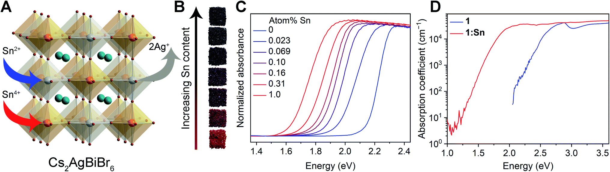 | ||
| Fig. 1 (A) The crystal structure of Cs2AgBiBr6 (1) and an illustration of the substitution mechanism of Sn in crystals to yield 1:Sn. Orange, gray, turquoise, and brown spheres represent Bi, Ag, Cs, and Br atoms, respectively. (B) Photographs of crystals of 1 and 1:Sn. (C) UV-vis absorbance spectra of crystals of 1 and 1:Sn converted from diffuse reflectance spectra using the Kubelka–Munk transformation. Atom% Sn was obtained from inductively coupled plasma analysis. (D) Photothermal deflection spectroscopy (PDS) scans collected on thin films of 1 and 1:Sn (4 atom% Sn; estimated from X-ray photoelectron spectroscopy). In the high-energy region (>3.0 eV), PDS and UV-vis absorbance data were combined after normalization. | ||
Photothermal deflection spectroscopy (PDS) was used to address the possibility that Sn alloying may, instead of reconstructing the bandgap, cause lattice disorder that creates weakly absorbing sub-bandgap trap states. PDS offers a wider dynamic range of absorption than UV-vis spectroscopy but requires samples with smooth surfaces with areas of several mm2. Thin films of 1 and 1:Sn were therefore used for these measurements. The films varied in color from yellow to brown with increasing Sn content (film thickness = 190 ± 16 nm). UV-vis transmission and reflectance measurements track this color change, showing increased low-energy absorption as a function of Sn content (Fig. S7†). PDS measurements on thin films revealed similarly large Urbach energies (70–100 meV) for both 1 and 1:Sn (4 atom%; Fig. 1D). Because 1 has an indirect bandgap, the absorption coefficient at the bandgap onset is small; sub-bandgap trap states that may form upon alloying may have similarly small absorption coefficients. Thus a redshift of the absorption onset, i.e., at low values of absorption coefficient (<104 cm−1), does not necessarily indicate a bandgap reduction, in contrast to lead perovskites with direct bandgaps.16,17,20,22,24,26 We therefore looked deeper into the bandgap, at energies where the absorption coefficient reaches ca. 104 cm−1. The PDS spectrum of 1:Sn reaches an absorption coefficient of 3 × 104 cm−1 at an energy ca. 0.7 eV lower than for 1, indicating that the observed absorption redshift arises from a bandgap reduction,31 as opposed to sub-bandgap trap states induced by the Sn impurities, which are not expected to affect these higher-energy transitions.
3. Sn speciation in the alloy
3.1. XANES analysis
Because Sn2+ is known to be oxidatively unstable in CsSnIIBr3,32 we sought to determine the oxidation state of Sn in 1:Sn. Comparing X-ray absorption near-edge structure (XANES) spectra collected at the Sn L3- and K-edges in 1:Sn (1 atom% Sn) to those of CsSnIIBr3 and Cs2SnIVBr6 perovskite standards indicated that Sn in 1:Sn was present in a mixture of 2+ and 4+ oxidation states in pulverized crystal samples that had been prepared and measured under inert atmosphere. Linear combination fitting of the XANES spectrum of 1:Sn to the XANES spectra of CsSnIIBr3 and Cs2SnIVBr6 standards indicated a mixture of Sn2+ and Sn4+ in ratios ranging from 7:1 to 3:2 Sn2+ to Sn4+ in several samples, with an average ratio of 2:1 Sn2+ to Sn4+ (Fig. 2A and S8†). The low signal-to-noise ratio at the Sn L3-edge due to the small concentration of Sn and lifetime broadening combined with the low energy resolution at the Sn K-edge precluded a more precise assignment of the ratio of Sn2+ to Sn4+. Although the host lattice of 1 in 1:Sn remains structurally unchanged with exposure to ambient atmosphere, the Sn2+ in 1:Sn is unstable to post-synthetic oxidation: exposure of a sample of pulverized crystals of 1:Sn to ambient atmosphere for 1 week resulted in a reduction of the ratio of Sn2+ to Sn4+ from 3:2 to 2:9 (Fig. S9†).
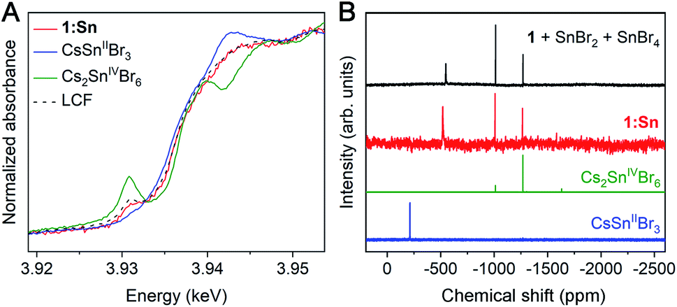 | ||
| Fig. 2 (A) Sn L3-edge XANES spectra of pulverized crystals of 1:Sn (1 atom% Sn) and CsSnIIBr3 and Cs2SnIVBr6 standards. LCF denotes a linear combination fit of the two standards' spectra to that of 1:Sn. (B) 119Sn NMR spectra of crystals of 1:Sn (1 atom% Sn), CsSnIIBr3, and Cs2SnIVBr6 dissolved in DMSO-d6 and of 1 dissolved in DMSO-d6 with SnBr2 and SnBr4 added to solution. | ||
3.2. Redox titration
The Sn2+ content of 1:Sn (1 atom% Sn) was determined to be 0.59(4) atom% by iodimetric titration on crystals digested in purified hydrobromic acid. Assuming a total Sn content of 1 atom%, as given by ICP analysis (Table S1 and Fig. S1†), gives a Sn2+ to Sn4+ ratio of ca. 3:2, in agreement with the XANES results range. Due to the variance of the total Sn content given by ICP analysis for the highest alloying level (1.0(2) atom% Sn, averaging over five samples), this ratio is taken to be an approximation.
3.3. 119Sn NMR
As an additional determination of the oxidation state ratio of Sn in 1:Sn we turned to 119Sn NMR. Magic-angle spinning solid-state 119Sn nuclear magnetic resonance (NMR) of CsSnIIBr3 and Cs2SnIVBr6 gave clear, relatively broad (FWHM ∼ 30 ppm) resonances at −370 and −1965 ppm, respectively. However, despite long (25–33 h) acquisition times, no signals were observed from crystals of 1:Sn (1 atom% Sn), likely due to the low concentration of Sn (Fig. S10†). We, therefore, collected solution-state 119Sn NMR spectra on crystals of 1:Sn (1 atom% Sn) dissolved in DMSO, which showed one broad peak at −520 ppm (FWHM ∼ 10 ppm) and two narrow peaks at −1010 and −1270 ppm (FWHM ∼ 1.5 ppm; Fig. 2B). The chemical shifts of the two upfield peaks match those of the two most intense peaks in the NMR spectrum of Cs2SnIVBr6 in DMSO. Though its chemical shift does not match that of the broad peak in the NMR spectrum of CsSnIIBr3 in DMSO, the broad peak is shifted downfield of the Sn4+ peaks, suggesting its origin to be Sn2+. Indeed, intentionally adding SnBr2 and SnBr4 to a solution of 1 in DMSO gives a spectrum that is a close match to that of 1:Sn (Fig. 2B). The change in chemical shift of the Sn2+ signal from the CsSnIIBr3 standard to the sample of 1:Sn spiked with SnBr2 and SnBr4 suggests that Ag and/or Bi interact with the Sn2+ in DMSO solution, altering the observed chemical shift. Peak integration of the spectrum of 1:Sn in DMSO gives an approximate ratio of 2:1 Sn2+ to Sn4+, in agreement with the results from XANES and redox titration. Given the agreement amongst these techniques, we assign an average ratio of 2:1 Sn2+ to Sn4+ in crystals of 1:Sn (1 atom% Sn). This ratio appears to vary from 7:1 to 3:2, likely based on subtle synthetic changes such as rates of crystallization.
3.4. Sn2+ oxidation
Although our syntheses were performed with Sn2+ precursors in inert atmosphere, we consistently see evidence for Sn4+ in crystals of 1:Sn. Attempts to prevent oxidation of Sn2+ by reagent purification and addition of hypophosphorous acid as a reducing agent were unsuccessful, indicating that the partial oxidation of Sn2+ is thermodynamically favorable in this system. Although the oxidant for Sn2+ in 1:Sn is yet unknown, the oxidized product Cs2SnIVX6 is reported to form in syntheses of CsSnIIX3 in hydrohalic acid, regardless of reagent purity.33 Indeed, the Sn 6s2 orbitals lie at the valence band maximum in 1:Sn and is most easily oxidized, similar to the case for ASnI3.34,35 At the other extreme, addition of SnBr4 to the crystallization solution for 1 resulted in the formation of 1 and Cs2SnIVBr6 and did not yield 1:Sn in the absence of SnBr2.4. Charge-compensating defects
4.1. Elemental composition
Given that heterovalent substitution of Sn in 1 was expected to produce charge-compensating vacancies, ICP-MS/ICP-OES were used to quantify the elemental composition of 1:Sn (Table S1 and Fig. S1†). The results showed a tunable quantity of Sn inclusion, up to ∼1 atom% in crystals, proportional to the concentration of SnBr2 in the precursor solution. As indicated by PXRD, the formation of a biphasic mixture of 1:Sn and the perovskite CsSnIIBr3 gives an upper bound to the Sn concentration achievable in phase-pure 1:Sn crystals (Fig. S11†). A slight shift of the PXRD pattern to higher angles is apparent in 1:Sn crystals, corresponding to a lattice parameter increase of up to ∼0.14%. The observed expansion is consistent with Sn alloying into 1, as the doubled lattice parameter of CsSnIIBr3 is 3% larger than the lattice parameter of 1. The ICP results also showed a modest decrease in Bi content and a substantial decrease in Ag content, more than the predicted value for a 1:1 substitution of Sn for Ag, suggesting that Ag vacancies are being formed as a charge-compensating mechanism with Sn alloying.
4.2. Lattice vacancies
Single-crystal X-ray diffraction (SC-XRD) also corroborates the formation of Ag vacancies upon Sn alloying. SC-XRD of 1:Sn (1 atom% Sn) showed a similar structure to that of 1 but with significant missing electron density at the Ag site when modelled with full Ag occupancy (Fig. 3A and Table S2†). Because Sn has a larger scattering factor than Ag, the missing electron density could not be attributed to Sn substitution at the Ag site. The missing electron density was instead assigned to Ag vacancies, consistent with the ICP results showing greater Ag loss than expected for a 1:1 substitution of Sn for Ag. Though the ICP results additionally show Bi loss with Sn alloying in 1:Sn, the low magnitude of this loss precludes detection by SC-XRD. Refining the Ag site in this model as having an equal concentration of Sn impurity atoms and vacant sites gave occupancy values of 86% Ag, 7.0% Sn, and 7.0% vacancies, similar to the experimentally determined concentrations of Ag and Sn in 1:Sn (1 atom% Sn). In order to probe for evidence of Bi vacancies, we attempted to obtain a single crystal with higher Sn content. Crystallizations with high concentrations of SnBr2 lead to mixtures of 1:Sn and CsSnIIBr3 crystals. Manually separating a single crystal of 1:Sn from this mixture allowed us to obtain the SC-XRD data of a crystal with a higher content of Sn than we could isolate from a phase-pure mixture. Refinement of these data gave a structure solution with significant missing electron density at the Ag site and, to a lesser extent, at the Bi site (Fig. 3B and Table S2†). Modelling mixed occupancy at the Ag site gave a Ag occupancy of 65% and Sn and vacancy occupancies each of 18%. Modelling the Bi site as an atomically mixed site with Sn gives occupancies of 84% for Bi and 16% for Sn. Alternatively, the missing electron density at the Bi site could be assigned to vacancy formation at that site or a combination of Sn substitution and vacancy formation.
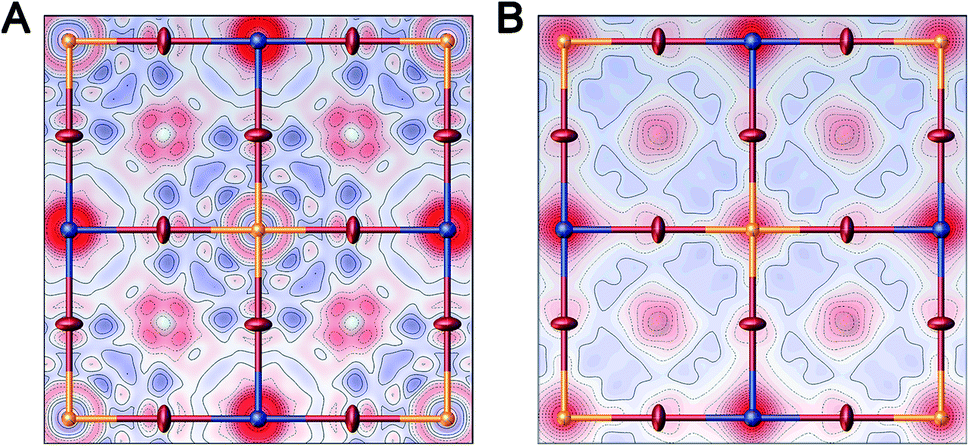 | ||
| Fig. 3 Projections of the (a, b) plane showing the differences between the calculated and observed structure factors for a SC-XRD solution of (A) 1:Sn (1 atom% Sn) and (B) 1:Sn selected from a phase-impure batch of crystals with a higher Sn alloying content (see text for details). Each solution was modeled with full Ag and Bi occupancies. Excess electron density in the model is shown in blue, while missing electron density is shown in red. Atoms of Br, Ag, and Bi are represented by the red, blue, and orange ellipsoids, respectively. The large electron density hole at the Ag sites in (A) and (B) is indicative of Ag vacancies, whereas the smaller electron density hole at the Bi site in (B) may be indicative of Bi vacancies, Sn substitution, or a combination of the two. | ||
The XANES, redox titration, NMR, ICP, and SC-XRD results, taken together, indicate that Sn2+ substitutes at the Ag+ site while Sn4+ substitutes at the Bi3+ site with an approximate ratio of 2:1 Sn2+ to Sn4+, collectively generating Ag+ vacancies as the primary charge-compensating defect (Fig. 1A). Similar charge-compensating metal cation vacancies have been observed in oxide perovskites upon heterovalent substitution.36 Though the participation of competing substitution mechanisms cannot be rigorously excluded, this model provides the best fit with the experimental data (Table S3†). We assume substitution of Sn2+ at the Ag+ site and Sn4+ at the Bi3+ site due to the large mismatch in valence between Sn4+ and Ag+. Additionally, substitution of Sn2+ at the Bi3+ site would require a positively charged compensating defect, such as a Br− vacancy, which is not supported by the ICP nor the SC-XRD results. The modest decrease of Bi content with Sn alloying suggests that there is no significant density of Bi vacancies in 1:Sn. We therefore propose the formula Cs2(Ag1−(2a+b)SnIIa)(Bi1−bSnIVb)Br6 for 1:Sn crystals, where 0.0023(1) < a + b < 0.10(2).
Similar to the host lattice 1, which exhibits only very weak photoluminescence, the alloyed material 1:Sn does not photoluminescence, consistent with its computed indirect bandgap. It is also possible that the lattice vacancies required for heterovalent alloying may act as nonradiative carrier recombination sites. Therefore, the carrier dynamics of 1:Sn should be studied to assess the feasibility of charge extraction from lattices containing metal cation vacancies.
5. Band structure
We calculated the band structures for 1:Sn to understand the electronic consequences of Sn2+ and Sn4+ alloying in 1. Our calculations were performed using density functional theory (DFT) within the generalized gradient approximation of Perdew, Burke, and Ernzerhof (PBE) as implemented in the VASP code.37,38 Spin–orbit coupling (SOC) effects were treated self-consistently. The calculated bandgap of an 80-atom supercell of 1 using this method is 1.11 eV (Fig. 4A), underestimating the experimental value of 1.95 eV, as is expected for DFT-PBE-SOC and consistent with past calculations from similar computations for (CH3NH3)PbI3.39 We note that in the band structure of the primitive unit cell, the valence band maximum is unfolded from Γ to X. Accurate prediction of bandgap energies requires a more rigorous treatment of exchange and correlation effects, including electron–hole interactions, that is currently prohibitive for the large unit cells considered here; however, our DFT-PBE-SOC calculations are expected to capture trends, sufficient for the present study (see ESI† for details).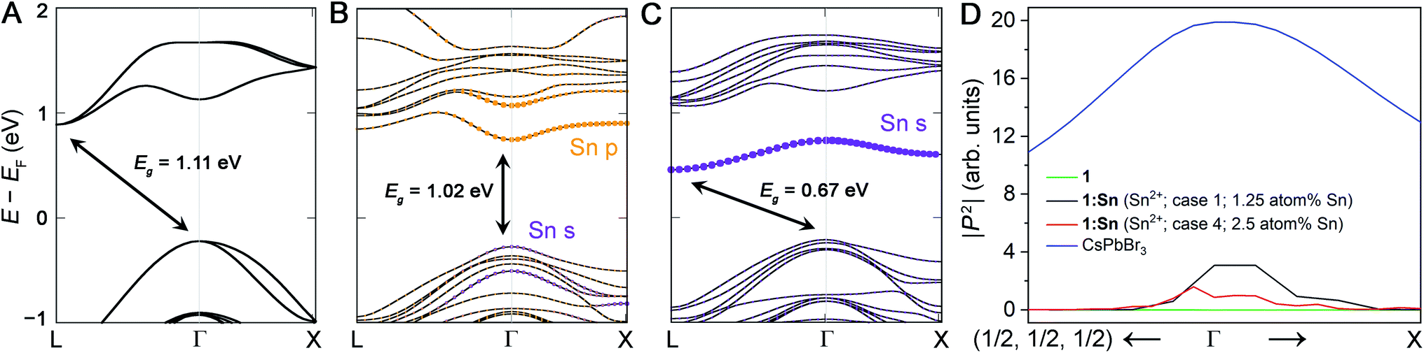 | ||
| Fig. 4 Computed band structures of 80-atom supercells of (A) 1, (B) 1:Sn (1.25 atom% Sn) with Sn2+ substitution at the Ag+ site and a vacancy at another Ag+ site, and (C) 1:Sn (1.25 atom% Sn) with Sn4+ substitution at the Bi3+ site and a vacancy at a Ag+ site. Projections of the Sn orbital character of the bands are shown in color. (D) The magnitude of the transition dipole matrix elements of direct transitions between the highest lying valence and lowest lying conduction band in the vicinity of Γ for 1, 1:Sn (alloying Cases 1 & 4, which are predicted to give direct gaps; see Section 5), and for CsPbBr3, a direct-bandgap perovskite. Equivalent k points are denoted; (1/2, 1/2, 1/2) corresponds to L and R in the double perovskites and in CsPbBr3, respectively. The range of k-points plotted is from (0, 0, 0) to (0.1, 0.1, 0.1), corresponding to the direction from Γ towards L or R, and from (0, 0, 0) to (0.1, 0.0, 0.1), corresponding to the direction from Γ towards X. | ||
For our DFT calculations of the bandgap of 1:Sn, we constructed supercells in which one or more of the B-site cations were substituted with Sn, where B-site refers to the octahedrally coordinated cation in the perovskite (Ag and Bi in 1). The insertion of heterovalent Sn—which may be considered to assume nominal charges of Sn2+ or Sn4+—into the structure of 1 necessitates a charge-compensating mechanism to maintain charge neutrality, such as the formation of cation vacancies. Because of the numerous permutations of possible substitution scenarios and the computational expense of using such large supercells, we used our experimental results to guide our choice of calculations: we considered four separate cases that could arise in nominal Sn2+ and Sn4+ substitutions, assuming the Sn atoms and vacancies substitute only at the Ag and Bi sites, consistent with our experimental evidence.
Case 1: two Ag atoms were removed and replaced with one Sn and one vacancy, respectively, to model nominal Sn2+ substitution at the Ag site with Ag vacancies as the charge-compensating defect. The supercell consisted of 80 atoms, corresponding to 1.25 atom% Sn substitution. In this supercell, there were 8 different Ag sites for substitution, thus 7 different relative arrangements of the Sn and vacancy on these sites were considered. For all arrangements, the lattice parameters and internal coordinates were relaxed (without spin–orbit coupling) until the forces were converged to 10 meV Å−1 (Tables S4–S6†). The arrangement with Sn and the vacancy occupying adjacent B-sites was computed to have the lowest energy (Table S7 and Fig. S12; see ESI† for details). The calculated band structure of this arrangement, including spin–orbit coupling, revealed a direct bandgap with a modest reduction of <0.1 eV from the DFT-PBE-SOC bandgap of 1 (Fig. 4B and S13†).
Case 2: one Bi atom was replaced with one Sn atom and one Ag vacancy was introduced to model nominal Sn4+ substitution at the Bi site with Ag vacancies as the charge-compensating defect. The supercell consisted of 80 atoms for a 1.25 atom% concentration of Sn. After considering several arrangements of the Sn and vacancy (see ESI† for details), the structure placing Sn and the vacancy at adjacent B-sites was computed to be the lowest-energy structure, similar to Case 1. In contrast to Case 1, Case 2 resulted in an indirect but substantially reduced DFT-PBE-SOC bandgap (by 0.44 eV), in reasonable agreement with the experimentally determined bandgap reduction of 0.5 eV in crystals of 1:Sn (1 atom% Sn; Fig. 4C and S14†). Note that whereas these calculations largely underestimate the absolute bandgap values, as expected, relative changes in bandgap can be well captured, and that is indeed what we find here.
Case 3: four Bi atoms were replaced with three Sn atoms and one vacancy to model nominal Sn4+ substitution at the Bi site with Bi vacancies as the charge-compensating defect. The supercell consisted of 160 atoms for a 1.875 atom% concentration of Sn. After comparing the DFT-PBE energies of 8 relaxed structures with substitutions on different Bi sites in the supercell, the lowest-energy configuration was computed to be one in which the Sn atoms and vacancy occupy adjacent sites, similar to the previous cases. The calculated DFT-PBE-SOC band structure in this scenario had a slightly indirect bandgap, while the conduction band had a very narrow bandwidth compared to the other cases. The bandgap was reduced by 0.61 eV compared to 1, in fair agreement with the experimentally determined reduction (Fig. S15†).
Case 4: one Ag and one Bi atom were each replaced with Sn atoms to model nominal Sn2+ substitution in equivalent concentrations at each B-site. The supercell consisted of 80 atoms, giving an overall concentration of 2.5 atom% Sn. The lowest-energy arrangement contained Sn atoms on adjacent Ag and Bi sites (see ESI† for details). A largely computational study of Pb2+ alloying in 1 proposes a similar mechanism.28 The DFT-PBE-SOC bandgap in this case was calculated to be direct, and reduced by 0.47 eV relative to the bandgap of 1 (Fig. S16†).
In Case 1, our DFT calculations indicate the direct bandgap results from the introduction of Sn 5p0 character and Sn 5s2 character at Γ. In contrast, in Case 2, the Sn substitution at the Bi site results in the introduction of a band below the CBM with Sn 5s0 character at L, resulting in a more reduced but slightly indirect bandgap (Fig. 4 and Table S8†). To confirm that the direct bandgap afforded by Sn2+ alloying contributes to optical absorption, we calculated the magnitudes of the transition dipole matrix elements in the independent particle approximation for 1, Sn2+-alloyed 1 (Cases 1 & 4), and the direct-bandgap semiconductor CsPbBr3 for comparison. Although the magnitudes of the transition dipole matrix elements for 1:Sn are smaller than those of CsPbBr3, they are significantly greater than the negligible magnitude for 1, supporting the presence of an optically active direct bandgap in Sn2+-alloyed 1 (Fig. 4D). We additionally calculated the imaginary part of the dielectric function as a function of energy in the independent particle approximation for 1 and Sn2+-alloyed 1 (Cases 1 & 4) to approximate their absorption spectra. These calculations show a clear redshift in the onset energy of the dielectric functions, offering further support for the bandgap reconstruction in Sn2+-alloyed 1 (Fig. S17†).
Because the 5s0 orbital from nominal Sn4+ substitutions is expected to be lower in energy than the 5p0 orbital from Sn2+ substitutions, a sample comprising both Sn2+ and Sn4+ in comparable amounts, as is the case for 1:Sn crystals, would therefore be expected to have a substantially reduced indirect bandgap. This was confirmed by a computation performed on a 320-atom supercell modelled to match this experimentally observed substitution pattern (Table S9 and Fig. S18†). At very low alloying concentrations, Sn impurities should act as isolated sub-bandgap trap states. With increasing concentration, impurity bands quickly form from the hybridization of Sn atoms with the host lattice. At higher concentrations of Sn, the defect bands become more dispersive, thus serving to fundamentally alter the electronic structure of 1, as corroborated through PDS measurements of 1:Sn films.
6. Alloying thin films
6.1. Sn content in films
The nature of the alloy may depend on material morphology and synthetic conditions. Therefore, in order to understand the effects of Sn alloying in 1 in the morphology relevant for devices, we studied thin films of 1:Sn. X-ray photoelectron spectroscopy (XPS) measurements indicated that a higher concentration of Sn could be alloyed into thin films compared to crystals, with PXRD showing that phase-purity was maintained up to ca. 4 atom% Sn—a 4-fold increase relative to crystals (Table S10, Fig. S19 and S20†). The PXRD data also revealed a slight lattice expansion of up to ∼0.52% with increasing Sn content, consistent with a ∼4-fold lattice expansion relative to crystals of 1:Sn (1 atom% Sn). The higher Sn content achievable in thin films of 1:Sn relative to crystals may arise from increased kinetic control offered by the faster film deposition methods, increased allowance for strain in these thin films, and the effect of changing the solvent from aqueous hydrobromic acid to DMSO.6.2. Film imaging
Thin films of 1 and 1:Sn were further characterized using scanning electron microscopy (SEM) and atomic force microscopy (AFM), revealing a change in morphology with inclusion of Sn (Fig. 5A, B and S21†). Whereas films of 1 have roughly spherical grains with an average size of 90 ± 30 nm and a root-mean-square (RMS) surface roughness of 15 nm, films of 1:Sn (4 atom% Sn) have irregularly shaped polydisperse grains with an average size of 100 ± 70 nm and a lower RMS surface roughness of 4 nm. Such changes in film morphology with alloying have been previously observed.40,41 Film thickness was measured by profilometry to be 190 ± 16 nm, independent of Sn content. To address the possibility of phase segregation of 1 and CsSnIIBr3 at the nanoscale, energy-dispersive X-ray spectroscopy (EDX) elemental mapping (Fig. 5C, S22, and S23†) and concentric backscatter imaging (CBS; Fig. S24†) were employed. EDX revealed a homogeneous distribution of Sn within a resolution of ∼500 nm while CBS and AFM showed homogeneous phases within resolutions of 25 nm and 8 nm, respectively.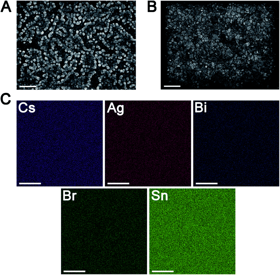 | ||
| Fig. 5 SEM images of thin films of (A) 1 and (B) 1:Sn (4 atom% Sn). (C) Elemental mapping on a thin film of 1:Sn (4 atom% Sn) using EDX. The scale bars in (A) and (B) are 500 nm and the scale bars in (C) are 2 μm. | ||
6.3. Sn speciation in films
As a further comparison between crystals and thin films of 1:Sn, XANES spectra were measured on thin films of 1:Sn of various alloying concentrations (Fig. S25†). Sn L3-edge XANES results indicated that the ratio of Sn2+ to Sn4+ decreased from nearly 1:0 at the highest achievable Sn concentration of 4 atom% to 4:1 at a Sn concentration of 2 atom% to 2:1 at a Sn concentration of 1 atom%, the same total Sn concentration as the maximum Sn concentration achievable in crystals. The agreement of the Sn2+ to Sn4+ ratios between thin film and crystal samples with 1 atom% alloyed Sn indicates that there is a thermodynamic driving force for partial oxidation of Sn2+ in 1:Sn, regardless of synthetic conditions and material morphology. Though the possibility of partial oxidation of Sn in 1:Sn from adventitious oxygen cannot be eliminated, rigorous precautions were taken to prevent such an occurrence. Intentional oxidation of a thin film of 1:Sn (4 atom% Sn) by exposure to ambient atmosphere overnight results in complete oxidation of the Sn2+ as determined by XANES (Fig. S26†). This oxidation occurs at an elevated rate relative to that for pulverized crystals likely due to an increased surface-area-to-volume ratio in films. SEM imaging of intentionally air-exposed thin films of 1:Sn revealed the presence of pillar-like surface features, identified by EDX elemental mapping to contain a highly elevated concentration of Ag and a moderately elevated concentration of Cs and O relative to the surrounding sample (Fig. S27 and S28†). Exposure of samples to dry air causes the formation of the pillar-like surface features, while exposure to wet nitrogen gas instead causes the formation of pinholes and the separation of grains, indicating that the formation of the surface features is connected to the oxidation of 1:Sn (Fig. S29†). Exposure of thin films of 1:Sn (4 atom% Sn) to ambient atmosphere over a period of hours results in a reversion of its brown color to the yellow color of thin films of 1.
7. Conclusions
We provide a detailed analysis of how the photophysical properties of crystals and thin films of the halide double perovskite Cs2AgBiBr6 (1) can be tuned through Sn alloying. XANES, redox titration, 119Sn NMR, ICP, and SC-XRD indicate that a ∼2:1 ratio of Sn2+ and Sn4+ is present in crystals of the alloyed perovskite (1:Sn; 1 atom% Sn) along with Ag+ vacancies. Our results are consistent with the following primary substitution pathway for crystals: Sn2+ substitutes at the Ag+ site while Sn4+ substitutes at the Bi3+ site, collectively generating anionic Ag+ vacancies as the dominant charge-compensating defect (see note on the Kröger–Vink notation below):42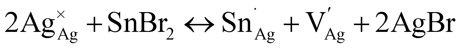

DFT calculations of the band structure show that the introduction of new bands with Sn4+ 5s0 impurity character below the conduction band minimum of the host lattice effects the large bandgap reduction seen in 1:Sn (1 atom% Sn), successfully mimicking the bandgap reduction resulting from Tl3+ incorporation in 18 in a nontoxic composition (Fig. 4).
Thin films of 1 can accommodate a higher Sn content (4 atom% Sn). In contrast to crystals, XANES measurements reveal the dominance of Sn2+ in thin films of 1:Sn (4 atom% Sn). This suggests a distinct alloying mechanism in thin films at high concentrations of Sn wherein only Sn2+ substitutes at both Ag+ and Bi3+ sites in approximately equal concentrations, thus maintaining overall charge neutrality (see Section 5, Case 4). Our computational results for this substitution pattern predominant in thin films show that, with a Sn concentration of 2.5 atom%, substitution of only Sn2+ at both Ag+ and Bi3+ sites in equal concentrations affords a direct bandgap (although an indirect transition is nearby, only 40 meV higher in energy) reduced by 0.5 eV from that of 1 (Fig. S16†), mimicking the indirect-to-direct bandgap change produced by Tl+ substitution8 in a nontoxic composition. Thus, heterovalent alloying further expands the considerable compositional diversity of double perovskites for finding functional analogs to the lead perovskites.
Conflicts of interest
There are no conflicts to declare.Acknowledgements
The experimental work was supported by the Department of Energy (DOE), Office of Basic Energy Sciences, Division of Materials Sciences and Engineering, under contract DE-AC02-76SF00515. We thank Dr Simon Teat, David Hanifi, Dr Stephen Lynch, and Rain Mariano for experimental assistance. SC-XRD experiments used the Stanford Nanocharacterization Laboratory (SNL) and beamline 11.3.1 at the Advanced Light Source (ALS). The ALS is a DOE Office of Science User Facility under contract no. DE-AC02-05CH11231. XPS measurements used the SNL and UV-vis and profilometry measurements used the Soft & Hybrid Materials Facility (SMF), both part of the Stanford Nano Shared Facilities (SNSF), supported by the National Science Foundation under award ECCS-1542152. XANES measurements used beamlines 4-1 and 4-3 at SSRL at the SLAC National Accelerator Laboratory. DFT calculations were supported by the US DOE, Office of Science, Office of Basic Energy Sciences (Theory of Materials FWP) Materials Sciences and Engineering Division (DE-AC02-05CH11231). Computational resources used at the Molecular Foundry were supported by the Office of Science, Office of Basic Energy Sciences, of the US DOE under contract no. DE-AC02-05CH11231. Additional computational resources were provided by NERSC.Notes and references
- A. Kojima, K. Teshima, Y. Shirai and T. Miyasaka, J. Am. Chem. Soc., 2009, 131, 6050–6051 CrossRef CAS PubMed.
- M. A. Green, A. Ho-Baillie and H. J. Snaith, Nat. Photonics, 2014, 8, 506–514 CrossRef CAS.
- A. Babayigit, A. Ethirajan, M. Muller and B. Conings, Nat. Mater., 2016, 15, 247–251 CrossRef CAS PubMed.
- A. H. Slavney, R. W. Smaha, I. C. Smith, A. Jaffe, D. Umeyama and H. I. Karunadasa, Inorg. Chem., 2017, 56, 46–55 CrossRef CAS PubMed.
- A. H. Slavney, T. Hu, A. M. Lindenberg and H. I. Karunadasa, J. Am. Chem. Soc., 2016, 138, 2138–2141 CrossRef CAS PubMed.
- E. T. McClure, M. R. Ball, W. Windl and P. M. Woodward, Chem. Mater., 2016, 28, 1348–1354 CrossRef CAS.
- G. Volonakis, M. R. Filip, A. A. Haghighirad, N. Sakai, B. Wenger, H. J. Snaith and F. Giustino, J. Phys. Chem. Lett., 2016, 7, 1254–1259 CrossRef CAS PubMed.
- A. H. Slavney, L. Leppert, D. Bartesaghi, A. Gold-Parker, M. F. Toney, T. J. Savenije, J. B. Neaton and H. I. Karunadasa, J. Am. Chem. Soc., 2017, 139, 5015–5018 CrossRef CAS PubMed.
- J. D. Donaldson, J. Silver, S. Hadjiminolis and S. D. Ross, Dalton Trans., 1975, 1500–1506 RSC.
- J. A. A. Ketelaar, A. A. Rietdijk and C. H. v. Staveren, Recl. Trav. Chim. Pays-Bas, 1937, 56, 907–908 CrossRef CAS.
- A. Spinelli, M. A. Torija, C. Liu, C. Jan and C. Leighton, Phys. Rev. B: Condens. Matter Mater. Phys., 2010, 81, 155110 CrossRef.
- K. Z. Fung, J. Chen and A. V. Virkar, J. Am. Ceram. Soc., 1993, 76, 2403–2418 CrossRef CAS.
- M. Maczka, A. Sieradzki, B. Bondzior, P. Deren, J. Hanuza and K. Hermanowicz, J. Mater. Chem. C, 2015, 3, 9337–9345 RSC.
- W. Eysel, H. H. Hofer, K. L. Keester and T. Hahn, Acta Crystallogr., Sect. B: Struct. Sci., 1985, 41, 5–11 CrossRef.
- N. Meethong, Y. H. Kao, S. A. Speakman and Y. M. Chiang, Adv. Funct. Mater., 2009, 19, 1060–1070 CrossRef CAS.
- A. L. Abdelhady, M. I. Saidaminov, B. Murali, V. Adinolfi, O. Voznyy, K. Katsiev, E. Alarousu, R. Comin, I. Dursun, L. Sinatra, E. H. Sargent, O. F. Mohammed and O. M. Bakr, J. Phys. Chem. Lett., 2016, 7, 295–301 CrossRef CAS PubMed.
- R. Begum, M. R. Parida, A. L. Abdelhady, B. Murali, N. M. Alyami, G. H. Ahmed, M. N. Hedhili, O. M. Bakr and O. F. Mohammed, J. Am. Chem. Soc., 2017, 139, 731–737 CrossRef CAS PubMed.
- Q. Chen, L. Chen, F. Ye, T. Zhao, F. Tang, A. Rajagopal, Z. Jiang, S. Jiang, A. K. Y. Jen, Y. Xie, J. Cai and L. Chen, Nano Lett., 2017, 17, 3231–3237 CrossRef CAS PubMed.
- K. Z. Du, X. M. Wang, Q. W. Han, Y. F. Yan and D. B. Mitzi, ACS Energy Lett., 2017, 2, 2486–2490 CrossRef CAS.
- X. Miao, T. Qiu, S. Zhang, H. Ma, Y. Hu, F. Bai and Z. Wu, J. Mater. Chem. C, 2017, 5, 4931–4939 RSC.
- M. Abdi-Jalebi, M. I. Dar, A. Sadhanala, S. P. Senanayak, M. Franckevičius, N. Arora, Y. Hu, M. K. Nazeeruddin, S. M. Zakeeruddin, M. Grätzel and R. H. Friend, Adv. Energy Mater., 2016, 6, 1502472 CrossRef.
- P. K. Nayak, M. Sendner, B. Wenger, Z. Wang, K. Sharma, A. J. Ramadan, R. Lovrincic, A. Pucci, P. K. Madhu and H. J. Snaith, J. Am. Chem. Soc., 2018, 140, 574–577 CrossRef CAS PubMed.
- Z. Y. Bin, J. W. Li, L. D. Wang and L. Duan, Energy Environ. Sci., 2016, 9, 3424–3428 RSC.
- Y. Yamada, M. Hoyano, R. Akashi, K. Oto and Y. Kanemitsu, J. Phys. Chem. Lett., 2017, 8, 5798–5803 CrossRef CAS PubMed.
- G. Li, T. Zhang, N. Guo, F. Xu, X. Qian and Y. Zhao, Angew. Chem., Int. Ed., 2016, 55, 13460–13464 CrossRef CAS PubMed.
- Z. Zhang, L. Ren, H. Yan, S. Guo, S. Wang, M. Wang and K. Jin, J. Phys. Chem. C, 2017, 121, 17436–17441 CrossRef CAS.
- Z. K. Wang, M. Li, Y. G. Yang, Y. Hu, H. Ma, X. Y. Gao and L. S. Liao, Adv. Mater., 2016, 28, 6695–6703 CrossRef CAS PubMed.
- J. Kangsabanik, V. Sugathan, A. Yadav, A. Yella and A. Alam, Phys. Rev. Mater., 2018, 2, 055401 CrossRef CAS.
- P. Kubelka and F. Z. Munk, Z. Tech. Phys., 1931, 12, 593–601 Search PubMed.
- A. H. Slavney, L. Leppert, A. Saldivar Valdes, D. Bartesaghi, T. J. Savenije, J. B. Neaton and H. I. Karunadasa, Angew. Chem., Int. Ed., 2018, 57, 12765–12770 CrossRef CAS PubMed.
- H. Angerer, D. Brunner, F. Freudenberg, O. Ambacher, M. Stutzmann, R. Höpler, T. Metzger, E. Born, G. Dollinger, A. Bergmaier, S. Karsch and H.-J. Körner, Appl. Phys. Lett., 1997, 71, 1504–1506 CrossRef CAS.
- S. Gupta, T. Bendikov, G. Hodes and D. Cahen, ACS Energy Lett., 2016, 1, 1028–1033 CrossRef CAS.
- H. Fuxin, CN Pat., CN 105523580 A, 2016.
- L.-y. Huang and W. R. L. Lambrecht, Phys. Rev. B: Condens. Matter Mater. Phys., 2013, 88, 165203 CrossRef.
- A. G. Kontos, A. Kaltzoglou, E. Siranidi, D. Palles, G. K. Angeli, M. K. Arfanis, V. Psycharis, Y. S. Raptis, E. I. Kamitsos, P. N. Trikalitis, C. C. Stoumpos, M. G. Kanatzidis and P. Falaras, Inorg. Chem., 2017, 56, 84–91 CrossRef CAS PubMed.
- H. M. Chan, M. R. Harmer and D. M. L. Smyth, J. Am. Ceram. Soc., 1986, 69, 507–510 CrossRef CAS.
- J. P. Perdew, K. Burke and M. Ernzerhof, Phys. Rev. Lett., 1996, 77, 3865–3868 CrossRef CAS PubMed.
- G. Kresse and J. Furthmüller, Phys. Rev. B: Condens. Matter Mater. Phys., 1996, 54, 11169–11186 CrossRef CAS PubMed.
- F. Brivio, K. T. Butler, A. Walsh and M. van Schilfgaarde, Phys. Rev. B: Condens. Matter Mater. Phys., 2014, 89, 155204 CrossRef.
- F. D. Paraguay, M. Miki-Yoshida, J. Morales, J. Solis and W. L. Estrada, Thin Solid Films, 2000, 373, 137–140 CrossRef.
- E. Yücel and Y. Yücel, Optik, 2017, 142, 82–89 CrossRef.
- According to the Kröger–Vink notation,
 refers to species A at site B in the crystal and vacancies are denoted as A = V. The effective charge of a defect is denoted as C = (·) for positive, (/) for negative, and (×) for neutral.

Footnote |
| † Electronic supplementary information (ESI) available: Experimental details, spectra, band structures, and crystallographic data. CCDC 1918859 and 1918860. For ESI and crystallographic data in CIF or other electronic format see DOI: 10.1039/c9sc02581b |
| This journal is © The Royal Society of Chemistry 2019 |