
 Open Access Article
 This Open Access Article is licensed under a Creative Commons Attribution-Non Commercial 3.0 Unported Licence
Energy storage: pseudocapacitance in prospect†
Cyrille
Costentin‡
 * and
Jean-Michel
Savéant
*
* and
Jean-Michel
Savéant
*
Université Paris Diderot, Sorbonne Paris Cité, Laboratoire d'Electrochimie Moléculaire, Unité Mixte de Recherche Université – CNRS No. 7591, Bâtiment Lavoisier, 15 rue Jean de Baïf, 75205 Paris Cedex 13, France. E-mail: cyrille.costentin@univ-paris-diderot.fr; saveant@univ-paris-diderot.fr
First published on 9th May 2019
Abstract
The two main types of charge storage devices – batteries and double layer charging capacitors – can be unambiguously distinguished from one another by the shape and scan rate dependence of their cyclic voltammetric current–potential (CV) responses. This is not the case with “pseudocapacitors” and with the notion of “pseudocapacitance”, as originally put forward by Conway et al. After insisting on the necessity of precisely defining “pseudocapacitance” as involving faradaic processes and having, at the same time, a capacitive signature, we discuss the modelling of “pseudocapacitive” responses, revisiting Conway's derivations and analysing critically the other contributions to the subject, leading unmistakably to the conclusion that “pseudocapacitors” are actually true capacitors and that “pseudocapacitance” is a basically incorrect notion. Taking cobalt oxide films as a tutorial example, we describe the way in which a (true) electrical double layer is built upon oxidation of the film in its insulating state up to an ohmic conducting state. The lessons drawn at this occasion are used to re-examine the classical oxides, RuO2, MnO2, TiO2, Nb2O5 and other examples of putative “pseudocapacitive” materials. Addressing the dynamics of charge storage—a key issue in the practice of power of the energy storage device—it is shown that ohmic potential drop in the pores is the governing factor rather than counter-ion diffusion as often asserted, based on incorrect diagnosis by means of scan rate variations in CV studies.
1. Introduction
Batteries and double layer capacitors are representative of the two main electrochemical means to store electrical energy.1 Faradaic processes are involved in the first case, i.e. electron transfer occurs across the electrode surface, and thus across the potential drop at the interface, to or from reactants present in solution or adsorbed at the electrode surface.2 In the second case, no faradaic process occurs, i.e., no charge transfer across the surface takes place. Charge storage is then simply the result of charging the electrochemical double layer at the interface between the base electrode and the surrounding solution.3Cyclic voltammetry (CV) offers a simple and eye-catching way of distinguishing between these cases (Fig. 1). This is the reason that this technique is referred to throughout the present discussion, noting that it has the same capabilities in terms of quantitative characterization as other electrochemical techniques such as galvanostatic and impedance techniques within equivalent time ranges. Double layer4 charging and discharging give rise to the classical capacitance charging CV-current–potential responses (ref. 5, pp. 14–16 and 353–357) as represented in Fig. 1a in a case where the double layer capacitance is approximately constant within the potential excursion range. The charging curve shows a quasi-rectangular shape and the whole curve is proportional to the scan rate.
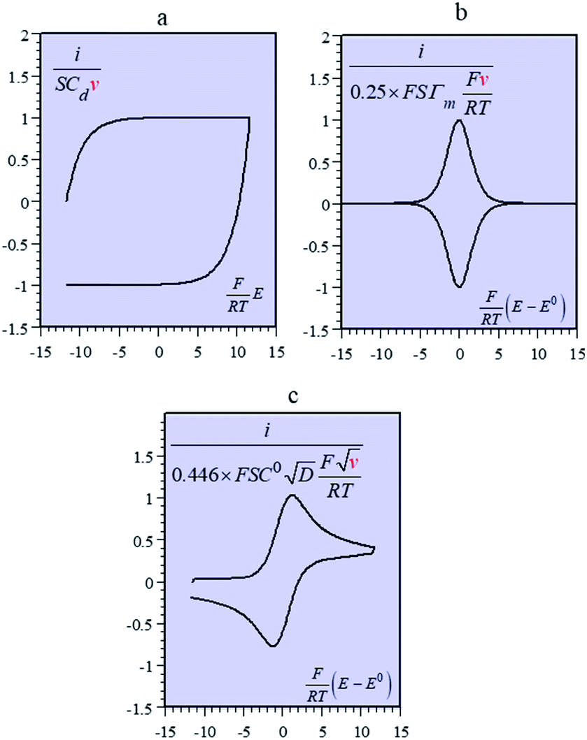 | ||
| Fig. 1 Cyclic voltammetric current–potential responses. i: current, E: electrode potential, E0: standard potential of the surface or solution redox couple, ν: scan rate, S: electrode surface area, F: Faraday, T: absolute temperature. (a) Double layer charging current (Cd: double layer differential capacitance). (b) Faradaic response of a surface redox couple (Γm: surface concentration, E0: standard potential of the surface redox couple). (c) Faradaic response of a solution redox couple (C0: solution concentration, E0: standard potential of the surface redox couple, D: reactant diffusion coefficient). | ||
Surface faradaic CV-current–potential responses, obtained with adsorbed reactants, are quite different in that they show peaks as represented in Fig. 1b.6 The peak current, like the capacitive plateau current, is proportional to the scan rate, but the difference in shape makes them readily distinguishable. However, the proportionality to the scan rate makes it possible to derive from the current response a formal capacitance obtained by simple division by the scan rate.
Solution faradaic CV-current–potential responses also display peak shapes (Fig. 1c) but the current is now under the dependence of reactant diffusion.7 Peak currents are then proportional to the square root of the scan rate. Distinguishing faradaic and double layer charging processes by means of their CV signatures thus raises no problem. This is not what happens with “pseudocapacitors” and with the notion of “pseudocapacitance”, as originally put forward by Conway et al.8 and defined as involving faradaic processes having, at the same time, a capacitive signature. Given the confusion that prevails regarding the notion of “pseudocapacitance”, we will start by setting up a precise definition of this notion. On this basis, we will then discuss the modelling of “pseudocapacitive” responses, first revisiting Conway's derivations and analysing critically the other contributions to the subject. We will then switch to an experimental example provided by the CV and structural characteristics of cobalt oxide films (CoPi). It will be the occasion to illustrate the way in which a (true) electrical double layer is built upon oxidation of the film in its insulating state up to an ohmic conducting state. The concentration of the buffer and the scan rate will be the two main operating parameters helping deciphering of the various phenomena at work. The lessons drawn at this occasion will then be used to re-examine the metal oxides, RuO2, MnO2, TiO2, Nb2O5… as classical putative examples of “pseudocapacitive” materials, taking into account their CV behavior and what can pertinently be said of their characteristics. More recently appearing promising materials like ‘MXenes’ will also be on the list. Study and application of these materials raise the interesting question of the dynamics of charge storage. Is it governed by counter-ion diffusion or rather the result of ohmic potential drop in the pores? This is the object of the last section together with the use of scan rate as a diagnostic tool in the attending CV studies.
2. The need of a precise definition of “pseudocapacitance”
In their Shakespearian-tone article, the authors of ref. 9 make two important remarks. (i) The term pseudocapacitive “should only be used for a given electrode investigated individually”. (ii) They also strongly emphasized that “the term “pseudocapacitance” is used to designate electrode materials (such as RuO2, MnO2) that have the electrochemical signature of a capacitive electrode (such as observed with activated carbons), i.e., exhibiting a linear dependence of the charge stored with the width of the potential window, but where charge storage originates from different reaction mechanisms”, leading to the quasi-rectangular form of the CV responses as shown in Fig. 1a. They particularly insist that systems like Ni(OH)2 and cobalt oxides in KOH electrolyte, which show battery type faradaic peaks, should not be considered to display a true pseudocapacitive behavior.3. Models attempting to account for a purely capacitive behavior that would be based on faradaic reactions
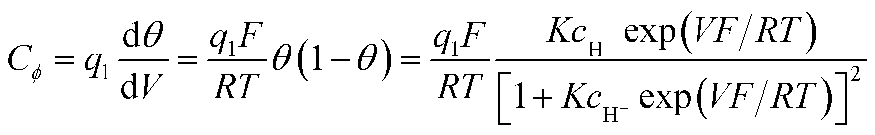
We fully adopt the above precise definition of “pseudocapacitance” in the following and discuss the models that attempt to account for a purely capacitive behavior that would be based on faradaic reactions. Honor to whom honor is due, we start with the work of Conway et al., as detailed in ref. 10, which provides a clear synthesis of their preceding contributions to the question.“From a thermodynamic point of view, pseudocapacitance originates whenever some property, y, proportional to charge passed, is related to potential by an equation of the form:
y/(1 − y) = K![[thin space (1/6-em)]](https://www.rsc.org/images/entities/char_2009.gif) exp(VF/RT) exp(VF/RT) | (1) |
The quantity y can be an extent of fractional coverage of an electrode surface (generated by the charge required for deposition of adatoms e.g., H at Pt, or metal adatoms in “underpotential deposition” reactions), an extent of fractional absorption, X, into some intercalation host (e.g., TiS2 or CoO2 accommodating Li), or third, some extent of conversion of an oxidized species to a reduced species (or vice versa) in a redox system in solution [e.g., aq. Fe(CN)64−/Fe(CN)63−] or one in a hydrous oxide, e.g., RuO2, IrO2, Co3O4. Each of the above types of examples corresponds in a formal general way to an electron transfer process between an oxidized species Ox (e.g., H+ or H2O, Li+, metal ion redox reagent) and a reduced species, Red (e.g., adsorbed H, Li+ in a host cathode lattice, metal ion in the reduced state in the redox reagent); thus Ox + ze ∼ Red. Pseudocapacitance arises when the extent of reaction, Q, is some continuous function of potential, V, so that a derivative, dQ/dV, arises that has the properties of a capacitance”.10
We may note that if y is a mere surface fractional coverage, with no special interaction of the adsorbed species with their neighbors, eqn (1) is just an expression of the Nernst law, whose application leads to the CV response shown in Fig. 1b. As seen before, this is a case where one can speak of formal capacitance (derived from a peaked curve) but certainly not of pseudocapacitance in the precise sense recalled earlier (quasi rectangular CV response as in Fig. 1a).
It would be tedious to examine successively all situations listed above that may complement this simple picture. For the moment, let's limit ourselves to the first and last examples of the list. We will come back to metal oxide examples later on.
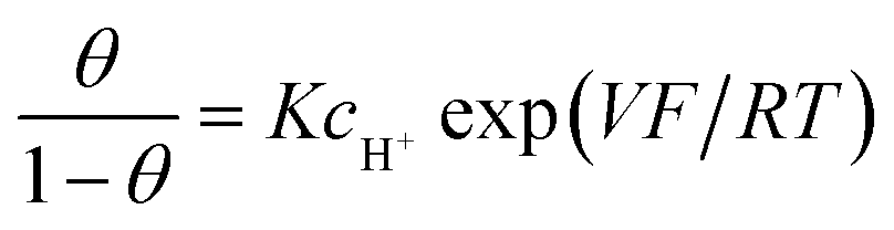
The first example is an “electrochemical surface process such as the so-called underpotential deposition of H [here “Ox” is H3O+ (or H2O) and “Red” is MHads]:
If adsorption obeys the simple Langmuir isotherm
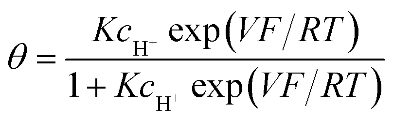
Then, a capacitance, qualified as “pseudocapacitance” in ref. 10 (pp. 222 and 223) can be obtained from:
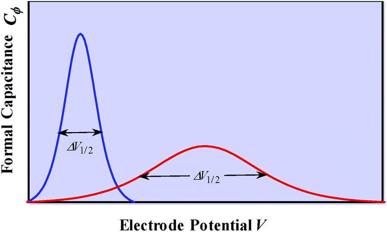 | ||
| Fig. 2 C ϕ vs. electrode potential profiles for an electrosorption process involving a zero (blue) and a positive (red) g value, i.e., for lateral repulsion. Adapted from Fig. 10.1 in ref. 10 p. 228, with permission. | ||
The next step consists of replacing the Langmuir isotherm using a Frumkin isotherm:
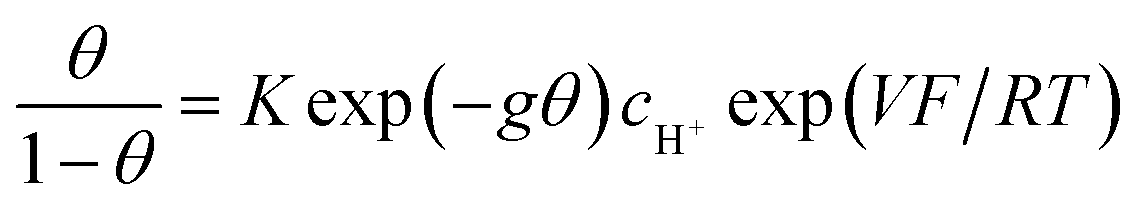
where θ is given by the above equation.
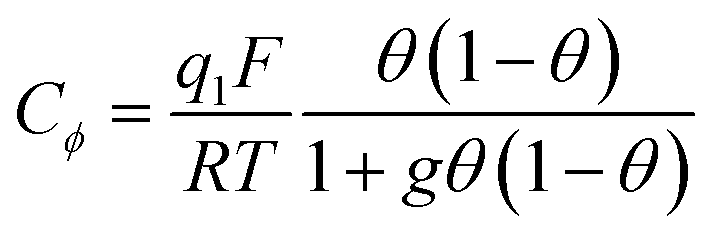
g > 0 corresponds to the expected repulsive interactions at the adsorbed state giving rise to the red capacitance vs. potential curve shown in Fig. 2. Although the peak is more spread out than when g = 0, we are still facing a peak-shaped curve, far from the quasi-rectangular response expected from a precisely defined “pseudocapacitance” curve (Fig. 1a).
For the second example, quote of the original work says: “Capacitors based on inorganic redox reagents also have a capacitance that is electrochemical rather than electrostatic in origin. Consider the following example:
| [Fe(CN)6]3− + e− ⇄ [Fe(CN)6]4−” |
Applying the Nernst law to this Ox + e− ⇄ Red couple, Conway et al. derived the “pseudocapacitances” represented in Fig. 3a and illustrated by the experimental CV curves shown in Fig. 3b. It clearly appears that these alleged “pseudocapacitances” have nothing to do with the actual “pseudocapacitances” precisely defined earlier and giving rise to the quasi rectangular CV responses of Fig. 1a.
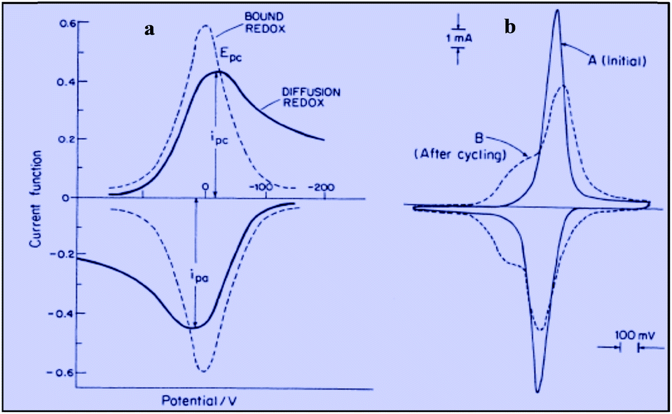 | ||
| Fig. 3 Cyclic voltammograms for the redox couple giving rise to pseudocapacitance: (a) free in solution (diffusion controlled) compared with surface bound; (b) experimental example of ferrocyanide bound on poly(vinylpyridine) (from Conway and Duic, unpublished). Adapted from Fig. 10.14 in ref. 10 pp. 250 and 251, with permission. | ||
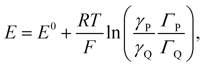
Coming back to the first example described above, the derivation developed for proton electrochemical reduction was recently revisited so as to obtain a general analysis applicable to any type of Ox(P) + e− ⇄ Red(Q) reaction.11 In the application of the Nernst law to the adsorbed P and Q species, taking into account, besides their surfaces concentrations, ΓP and ΓQ, their activity coefficients, γP and γQ:
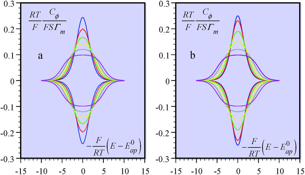 | ||
| Fig. 4 Formal capacitance Cϕvs. electrode potential as a function of the parameter 2(aQ + aP − 2aPQ) = FΔE0/RT = 0.1 (blue), 1 (red), 2 (green), 3 (yellow), 4 (gray), and 5 (magenta). (a) Calculated from interaction coefficients, aP, aQ and aPQ linearly varying with the surface concentrations. (b) Calculated from the square standard potential distribution. | ||
Positive values of the interaction parameters entail broadening of the capacitive responses as was very similarly the case in the first Conway et al. example. This shows again, but in a more general manner, that such putative “pseudocapacitances” are not compatible with the precise definition given earlier, which corresponds to the quasi rectangular CV responses of Fig. 1a.
It is also possible to show that a closely equivalent behaviour is found upon considering the superposition of several overlapping redox couples early “believed”8c to be at the origin of “pseudocapacitances”. This is defined as an equally distributed set of standard potentials, ranging from −ΔE0 to ΔE0 and centred at E0ap, the probability of each being (2FΔE0/RT) − 1, with FΔE0/RT = 2(aQ + aP − 2aPQ) (only considering positive values of FΔE0/RT = 2(aQ + aP − 2aPQ)). The apparent “pseudocapacitances” derived in this way (Fig. 4b) are very similar to those obtained from the first method, leading to the same conclusion.
Before concluding this section, we mention in the ESI† two picturesque albeit perfectly fanciful descriptions of the construction of a “pseudocapacitance” from faradaic reactions.12,13 It seems also worth discussing (still in the ESI†) another problematic modelling of quasi-rectangular capacitive-looking CV responses by summation of the successive faradaic contributions.14
4. A tutorial experimental example: cobalt oxide films in the presence of phosphate
Besides being valuable catalysts for water oxidation, cobalt oxide films (CoPi) deposited on electrodes15–17 show interesting properties related to the “pseudocapacitance issue”.11 The typical cyclic voltammetry (CV) response shown in Fig. 5 allows the delineation of several successive potential domains, namely in the negative-to-positive direction, an insulator zone, followed by a transition to a conductor zone before reaching the water oxidation catalytic wave.18 In the conductor zone, small peaks appear on top of the capacitive response. They represent surface proton-coupled faradaic waves, whose height can be modulated by the amount of buffer present in the solution. Fig. 6 shows the capacitive responses obtained when the amount of buffer has been decreased to a minimum, just required to maintain the bulk pH. The quasi-rectangular response thus obtained fits the idea that we are dealing with a true capacitance involving the double layer built at the interface between the solution and the oxide film, which behaves as an ohmic conductor in this potential range. The observed variation of the capacitance with the film thickness points to the idea that the film possesses a meso-to-nano structure responsible for the expansion of the actual surface area of the interface leading to respectable values of the capacitance here and for other metal oxides.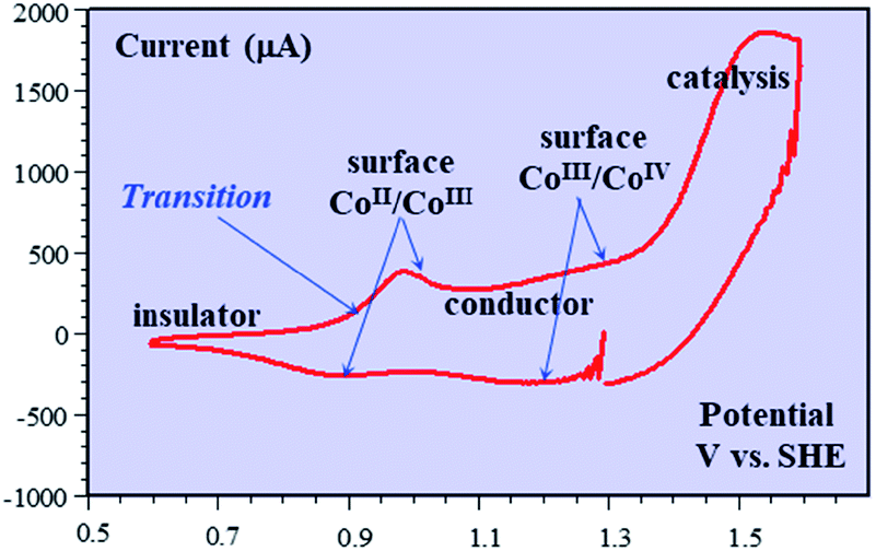 | ||
| Fig. 5 Cyclic voltammetry current–potential responses (potential: 1.29 → 0.59 → 1.59 → 1.29 V vs. SHE) at 8 V s−1 of a 39 nm cobalt oxide deposited (CoPi) film in the presence of 0.2 M potassium phosphate (KPi) at pH = 7. Adapted from Fig. 2 in ref. 18 with permission. | ||
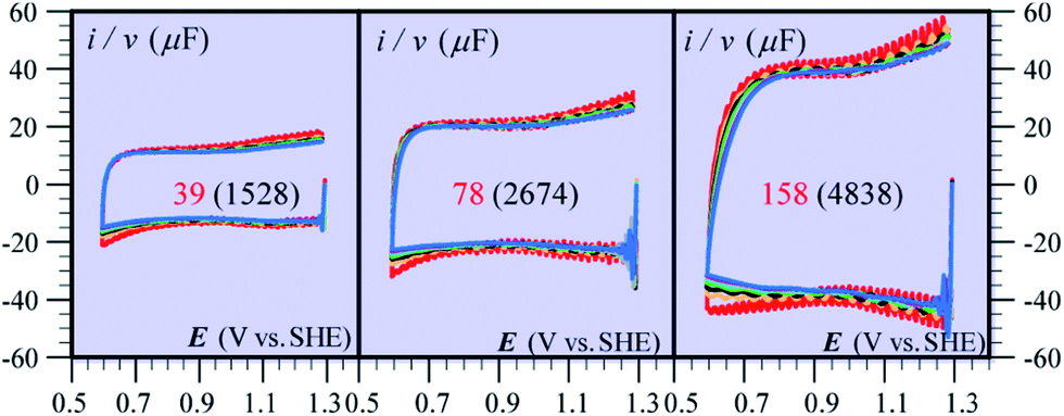 | ||
| Fig. 6 Cyclic voltammetry current–potential responses at various scan rates (ν) of CoPi films at pH 7 in the presence of 1 mM Pi and 100 mM KNO3. ν (V s−1): 1 (red), 2 (orange), 3 (black), 4 (green), 5 (cyan), 6 (gray), 7 (magenta), and 8 (blue). The numbers on each diagram are the values of film thickness in nm and, between parentheses, the value of the plateau capacitance in μF cm−2. Adapted from ref. 18, with permission. | ||
A further interesting question is the way in which this ohmic conductor status of the film is built up when the potential is moved positively from the isolator zone, entailing the faradaic oxidation of the material, most likely coupled with proton transfer. Fig. 7 shows various CV responses in the aforementioned transition zone (more data can be found in ref. 19).
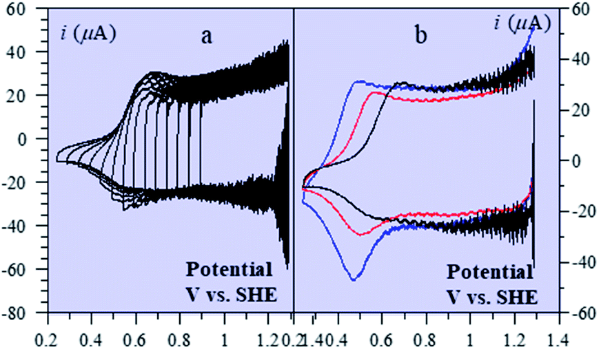 | ||
| Fig. 7 (a) CV of a 39 nm CoPi film in 1 mM KPi, pH = 7, and 100 mM KNO3. Scans are initiated at 1.29 V vs. SHE in the cathodic direction and inversion potential is varying. ν = 2 V s−1. (b) CV of a 39 nm CoPi film in the presence of 100 mM KNO3 and 1 mM KPi, pH 7. Scans are initiated at 1.29 V vs. SHE in the cathodic direction. ν = 2 V s−1. Films were deposited from different buffers: 100 mM KPi, pH 7 (black), 100 mM KHCO3, pH 10.3 (red), 100 mM KBi (blue), pH 9.2 (dots). | ||
Starting from the structural description of electrodeposited amorphous cobalt oxide films obtained from AFM images and X-ray atomic pair distributions schematically displayed in Fig. 8, we focus attention on the nanoclusters shown in Fig. 8b, and inside them, on the cobaltate phase, whose internal (Galvani) potential is denoted as ϕ whereas the Galvani potential of the bathing solution is denoted as ϕS.
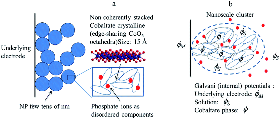 | ||
| Fig. 8 (a) Structural sketch of cobalt oxide electrodeposited films. (b) Scheme of the various phases considered in the electrochemical description of a cobalt oxide electrodeposited. Adapted from Fig. 4 in ref. 18 with permission. | ||
Noting p the density of holes and N the density of electronic states in the cobaltate phase, the electrode potential, at equilibrium may be expressed as:

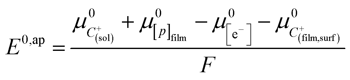
where the μ0's are the standard chemical potentials, the a's the activities and the γ's the activity coefficients (C+ represents a formal cation leaving the surface of the conductive phase surface to compensate the charge generated by oxidation of this phase). Considering activity coefficients as linear functions of the surface concentrations amounts to considering a simple square distribution of electronic states in agreement with what has been described earlier in the text and represented by Fig. 4b. The above equation may thus be recast as:
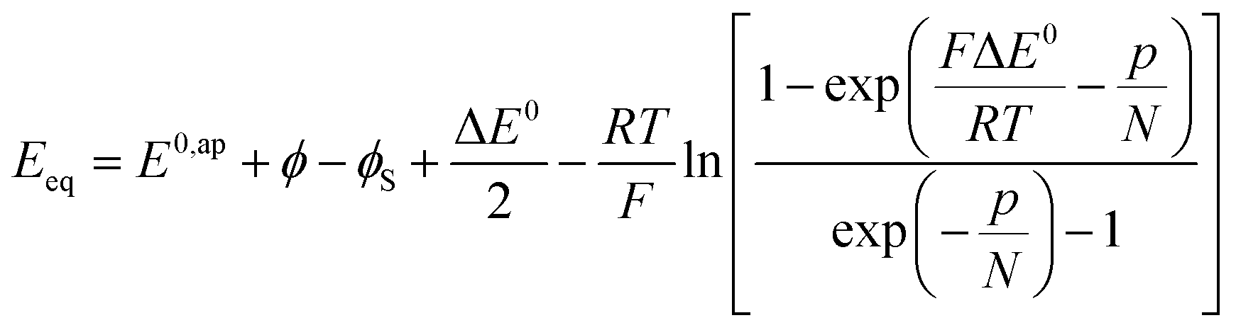
As the electrode potential E is raised starting from a situation where the “cobaltate phase” is not electronically conductive (p → 0 and ϕ = ϕS), the faradaic current flowing entails an increase of the density of free charge carriers (p) in the cobaltate phase. This process is usually referred to as charging the chemical capacitance of the film.20ϕS remains equal to the constant solution Galvani potential while ϕ is changing. Via charge compensation upon film oxidation, the charge distribution has been altered so that a gradient of electrical potential is created at the cobaltate phase/solution interface which now behaves as a double-layer capacitance and the corresponding charge transfer is a capacitive current. This phenomenon is usually referred to as band unpinning.21 Upon variation of the electrode potential E, the Galvani potential ϕ and the density of charge p are changing according to:
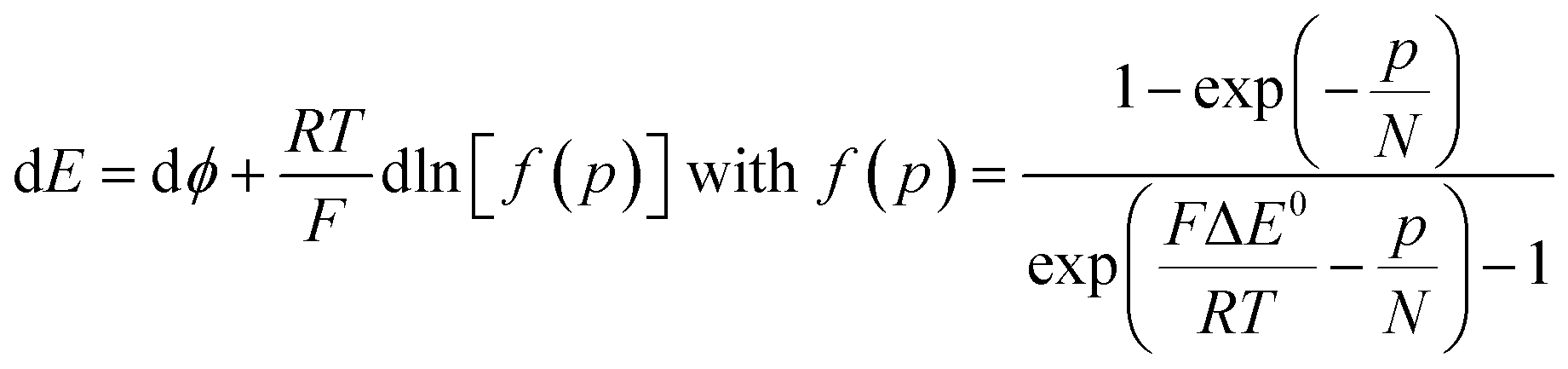
Thus, noting the capacitance Cd:
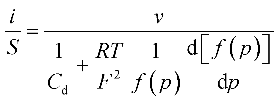
The system appears as equivalent to charging two series capacitances.21Fig. 9 thus shows a typical forward CV scan starting in the insulator region and the corresponding change of the film inner potential ϕ. The current initially increases exponentially reflecting the fact that it is essentially governed by the chemical capacitance charging, viz., a faradaic-type process, with the inner potential of the cobaltate phase remaining close to ϕS. Then, as the chemical capacitance increases, the current plateaus out, being then controlled by the capacitance charging while the inner potential rises accordingly. The film then behaves as an ohmic conductor.
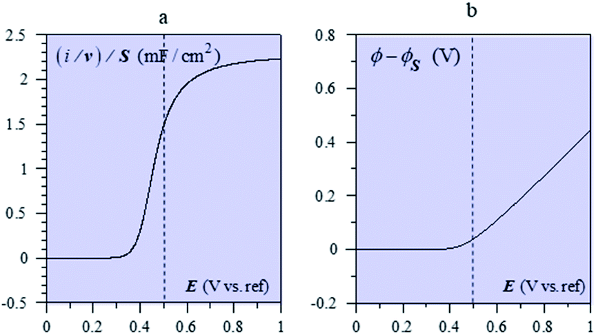 | ||
| Fig. 9 (a) Forward CV scan for with Cd = 2.55 mF cm−2 (i.e. capacitance of a 40 nm CoPi film), F2N/RT = 20 mF cm−2 (i.e. N = 8 × 1020 cm−3 for a 40 nm film), E0,ap − ΔE0/2 + ϕS = 0.5 V (dashed vertical line), T = 298 K. (b) Evolution of the film inner potential. Adapted from Fig. 5 in ref. 19 with permission. | ||
5. Other metal oxide materials and analogous films
Ruthenium dioxide is an emblematic example of a “pseudocapacitive” metal oxide material and the first to be reported as such.22 It is shown that films thermally prepared or obtained from single crystal RuO2 behave differently in cyclic voltammetry. The first ones show a rectangular response while the others show an ill-defined wave. A few years later, it was observed that, in the anodic region, a rectangular CV response is obtained after completion of several cycles of ruthenized Pt electrodes.23 It was thus inferred that, in the range of potentials where Ru is covered by an oxide film, a continuous change of the Ru standard potential due to interactions between redox centres may be responsible for such a behaviour thus grounding qualitatively the notion of transition metal oxide “pseudocapacitance”. Decades later, it was confirmed that RuO2 films exhibit different CV responses depending on the preparation method, thus pointing to the idea that the film structure is likely to be a crucial factor.24,25 For example, electrodeposited films show a broad reversible wave attributed to a faradaic Ru4+/Ru3+ redox process as confirmed by in situ X-ray spectroscopic studies probing the local structure.26 However, acknowledging that RuO2 is a metallic conductor27 and that hydrous RuO2 films exhibit a capacitive-like CV response, it was pointed out28 that understanding this behavior requires a description of the structure below the sub-nanometer range, which was not reachable with previously used X-ray techniques (EXAFS or XAFS).26 A further atomic pair-density function (PDF) analysis28 demonstrated that the medium-range structure of hydrated ruthenium oxide (RuO2·xH2O) can be described as a network of nanocrystals or clusters (1.2–2 nm) with water chemisorbed and physisorbed on the surface of the grains. Percolation paths between nanocrystals must be present for long range electronic conductivity. Such a picture matches our description of pseudocapacitors as true capacitors. Furthermore, the same study showed that capacitive properties vary upon changing hydration and hence the RuO2·xH2O local structure, as water is added or removed. Still, this new structural description of hydrous RuO2, in agreement with a capacitive CV behaviour, had to be reconciled with the faradaic behaviour of electrodeposited RuO2 films.22 It was then reported that annealing RuO2 films leads to an evolution of the CV response from a broad faradaic-type CV wave to an ideal capacitive rectangular type CV.29 The effect of such a temperature treatment was later confirmed (Fig. 10a)30 and assigned to the removal of bound water upon increasing temperature, thus promoting electronic conduction between RuO2 particles, which initially gives rise to a broad faradaic reversible wave. This is consonant with our model as description of the transition between a distribution of standard potentials and an electronic conduction band.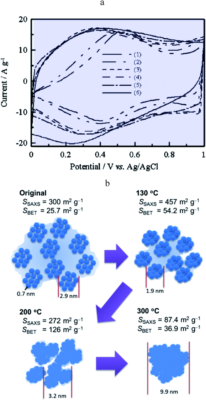 | ||
| Fig. 10 0(a) CV curves of (1) pristine RuOx·nH2O and RuOx·nH2O annealed in air for 2 h at (2) 150, (3) 200, (5) 350 and (6) 400 °C. CV curves were measured in 0.1 M H2SO4 at 25 mV s−1 from ref. 29 with permission. (b) Schematic diagram of the hierarchical nanostructure in RuOx·nH2O changing with the annealing temperature from ref. 32 with permission. | ||
We note, en passant, that WO3 films behave similarly. Anhydrous WO3 gives a peak-shaped faradaic CV response whereas hydrous WO3 exhibits a capacitive-type response together with an insulator–conductor transition as described earlier in the case of cobalt oxide films.31
A Small-Angle X-ray Scattering (SAXS) in situ study provided additional structural support to the description of the transition from a faradaic wave to a capacitive response upon annealing hydrous RuO2 (Fig. 10b).32 Indeed, prior to annealing, hydrous RuO2 is made of 0.7 nm clusters forming loose aggregates dispersed in a large amount of confined water. It is thus akin to an assembly of molecules characterized by a standard potential, leading, as expected, to a faradaic type CV response. Annealing densifies loose aggregates, inducing growth of RuO2 particles so as to generate a porous conductive network. At high temperatures (300 °C) most of the confined water has been extracted. Bare RuO2 domains thus aggregate to form large particles inducing a decrease of the capacitance. Once the conductive network is formed, the surface area of the aggregates governs the double-layer capacitance. Additional contribution of faradaic processes originates from Ru4+/Ru3+ redox conversion at the outermost layer of RuO2 aggregates. A similar picture is given in ref. 33, which depicts three contributions to the CV current, namely, a large charging current due to formation of a double layer in the pores, a reversible faradaic-type contribution due to ion specific electrosorption and an irreversible faradaic contribution due to hydrogen evolution or oxygen evolution occurring at grain-boundaries. Further theoretical calculations support the above description of conduction in RuO2 as involving an electronic band structure rather than localized redox states.34
Although theoretically interesting, ruthenium dioxide is too rare and expensive for practical applications. Manganese dioxide consequently attracted a lot of interest when it was reported to show a capacitive behavior.35 The case is, however, far from being simple as it can also exhibit almost purely faradaic CV responses as expected for a typical component of non-rechargeable batteries.36 Over the past twenty years, variable CV shapes have been reported (from faradaic to capacitive or a mix of both) depending on crystallinity,37 microstructure,38 electrolyte39 or doping species.40 It is however not obvious to draw a direct correlation between these various factors and the CV responses although it appears that charge storage in MnO2 possibly involves insertion/deintercalation of ions in the structure even in the absence of faradaic waves.41 Such a process is indicative of the lack of phase changing upon charging, owing to the absence of strong energy interactions between the intercalated ion and the bulk material. It would thus be equivalent to the charging of a large surface compact double-layer in the absence of a diffuse double layer.42 Nonetheless, two arguments have been put forward to support the assertion that the charging/discharging process is actually not capacitive but rather faradaic despite a quasi-rectangular CV response: (i) observation of ex situ XPS43 and in situ XAS spectroscopic changes associated with the Mn4+/3+ transition upon charging/discharging;44 (ii) gas adsorption (Brunauer–Emmett–Teller, BET) surface area too small to account for the observed capacitance, taking as intrinsic differential capacitance, 20 μF cm−2 (a typical value for conducting planar electrodes). It can however be counter argued that XPS ex situ analysis does not allow a sound correlation with the CV experiment since measurements are performed after one hour drying out of the film in air. In situ XAS analyses have led to variable results ranging from a small variation of the manganese oxidation number (3.71 to 3.98 over one volt polarization)45 to a larger variation (3.3 to 3.9).43 Having in mind that 20 μF cm−2 capacitance for a planar metallic electrode corresponds to ca. one electron stored over one volt per 10 metal surface atoms, it is not surprising to observe a variation of the average oxidation number of Mn centers if the porosity of the structure is so large that almost all Mn centers are to be considered as part of the electronically conductive phase surface and ions and solvent molecules intercalated in layers or in tunnels as an ionic conductive phase.41,46,47 The presence of inserted solvent molecules has been argued to be responsible for the lack of correlation between the BET surface area and the capacitance in the case of RuO2.32 This is also likely to be the case with MnO2. We may finally note that a Mn4+/Mn3+ faradaic description of the MnO2 charging process leads to a theoretical maximal charge of 1110 C g−1 which corresponds to 1230 F g−1 capacitance for a 0.9 V window. This value has been reached43 or even overpassed43 without observing the tailing of the CV response at the extreme potential limits (see Fig. 4), expected in the case of a faradaic process. This observation completes the ruling out of the faradaic description of quasi-rectangular CV responses and hence the fundamental incorrectness of the notion of “pseudocapacitance” as precisely defined at the beginning of the present perspective.
Nanoporous titanium dioxide (TiO2) based semiconductive electrodes have been widely studied because of their electrical, optical and chemical properties.48 Their electrochemical behavior is very similar to that of the cobalt oxide described earlier with the difference that cobalt oxide is a p-type semiconductor whereas TiO2 is an n-type semiconductor. TiO2 films are insulators when the Fermi level lies in the bandgap. Upon cathodic polarization a transition to a conductive behavior is observed, the charging process being ultimately controlled by a capacitive process referred to as band unpinning.21,49 Conductivity measurements also support this description50 as it was also the case for cobalt oxide films.51 Furthermore, it has been recently evidenced that, once polarized in the conductive domain, nanoporous TiO2 can massively insert protons leading to a large faradaic wave on top of the capacitive current,52 again showing the differences between both processes with no need of the notion of “pseudocapacitance”.
Initially studied for its electrochromic properties Nb2O5 was later recognized as a material for Li+ insertion.53 It was also reported that mesoporous Nb2O5 with nanoscale order exhibits a high charging capacity. CV reveals an increase of the cathodic current at ca. 2 V vs. Li/Li+ leading to a quasi-plateau shaped wave (proportional to the scan rate at low scan rates). Crystallinity seems critical to achieve large charge storage, presumably because the interlayer gaps are then accessible to cations.54,55 This behaviour is reminiscent of the insulator-to-conductor transition described in Fig. 9 for cobalt oxide, the observed high capacitance being the result of the porosity involving the interlayer gaps. Available CV data56,57 show a broad faradaic wave mixed with a capacitive component. Procedures used at this occasion to deconvolute the two contributions, based on the variation of the CV responses with the scan rate, are grossly incorrect as discussed in a further section, preventing any reliable conclusion to be drawn as to the mechanism of charge storage. Recent in operando Raman spectroscopy experiments associated with theoretical calculations58 have shown that Li+ ions intercalate in T-Nb2O5 within loosely packed layers and can move without passing through cramped space. Furthermore, the differences in adsorption energies of Li+ at different sites within the interspaces are small and thus incorporated lithium ions are not trapped in fixed locations. This picture can explain the capacitive response in cyclic voltammetry if combined with an electronic conductive behavior of the Nb2O5 quasi-2D network, without recourse, once more to the notion of “pseudocapacitance”.
Two-dimensional solids have attracted a lot of attention in recent years as energy storage systems owing to their large electrochemically active surface.59 Among them, ‘MXenes’ are a class of compounds of general formula Mn+1XnTx (n = 1–3), where M represents an early transition metal, X is carbon or nitrogen and Tx corresponds to surface terminations such as hydroxyl, oxygen or fluorine.60 “MXenes” can exhibit quasi-rectangular CV responses61 or show peaks62 depending on their structure as well as on the electrolyte used. Electrochemical quartz-crystal admittance studies combined with electronic conductance measurements have led to the conclusion that cation insertion in layers, similar to ion adsorption at the solid–liquid interface is responsible for the large charge storage on Ti3C2Tx characterized by quasi-rectangular CV responses.63 A double-layer charging mechanism was excluded to rationalize these results because the specific surface area was deemed too low, leading to the description of charge storage as “pseudocapacitive”. While not following the classical Gouy–Chapman–Stern4 model, the charging process may nevertheless be of the capacitive type. In situ XAS experiments indeed show that the Ti oxidation number is changing by only 0.1 unit over a 0.7 V window in line with the absence of faradaic peaks.64 In a non-aqueous electrolyte, counter ions hybridize with the orbitals of the surface MXene termination groups and faradaic peaks are accordingly observed.65 It follows that, in the case of MXenes also, the notion of “pseudocapacitance” does not hold, noting that the capacitive process differs from the classical Gouy–Chapman–Stern model, because of their microstructure.66,67
6. Charging time and power of the energy storage device
Disclosing the factors that govern the charging time is the key to understanding and improving power of the energy storage device in the context of porous structures. Since, as discussed earlier, “pseudocapacitive” materials behave just as genuine capacitors, their dynamics may be analyzed on the same grounds as standard capacitors such as porous carbon films. One central issue in this respect is the role of counter ion diffusion as opposed to that of ohmic drop in pores. It is first important to recall that the interface between an electronic conductor and an ionic solution displays a compact and a diffuse double layer as shown in Fig. 11.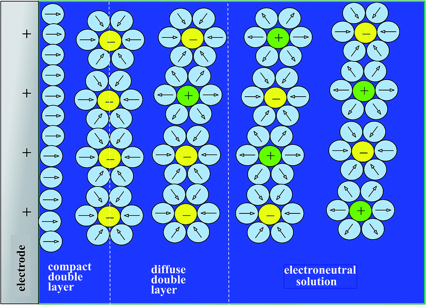 | ||
| Fig. 11 The electrochemical double layer. | ||
Analysis of the time response in the case of a planar electrode configuration shows that ion diffusion that may accompany the formation or changes of the double layer is much too rapid to influence the CV current–potential responses within the range of scan rates accessible in practice.68 The response thus follows a simple RC circuit representation. How is the description modified upon passing to porous electrode materials? Fig. 12 gives a schematic representation of a bi-hierarchical structure of such materials. The nanopores, if any, contribute to the overall capacitance but only through the charge imprisoned in compact double layers.
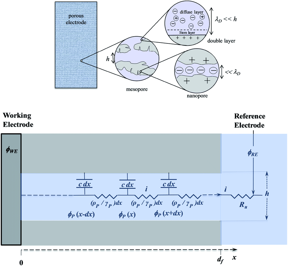 | ||
| Fig. 12 Top: Schematic representation of a bi-hierarchical structure of a porous electrode film with nanopores and mesopores; h = mesopores average size, λD: Debye screening distance (of the order of 1–10 nm). Bottom: Transmission line model applied to mesopores. ϕsubscript: potentials, i: current flowing through the film, distributed resistance and capacitance parameters of the equivalent transmission line: ρP: resistivity of the ionic solution, γP: fraction of the base electrode covered by the pore ends, Ru: resistance of the solution, c: capacitance per unit volume of the film, x: distance from the base electrode, df: thickness of the film. | ||
As to the larger pores—the mesopores—the effect of ion diffusion may be neglected for the same reason as given earlier in the case of planar electrodes. The CV responses are thus governed by potential ohmic drop in the pores (and to a lesser extent in the solution), which can be modelled according to a transmission line model, as summarized in bottom Fig. 12.
Fig. 13 shows some typical CV responses. The response time of the porous electrode is tf = RfCf, where Rf and Cf are the total resistance and capacitance of the porous electrode. In cases where the resistance in the solution outside the pores is negligible, as in the cases represented in Fig. 13, the CV responses depend on a single parameter, namely tf/tv with tv = (Ef − Ei)/ν (Ef and Ei being respectively the inversion and initial potential of the CV scan), which is a means of expressing the effect of scan rate in a dimensionless manner as in Fig. 14, and notably the fact that reaching the plateau value is more and more delayed as the scan rate is increased, with all other experimental parameters remaining the same.
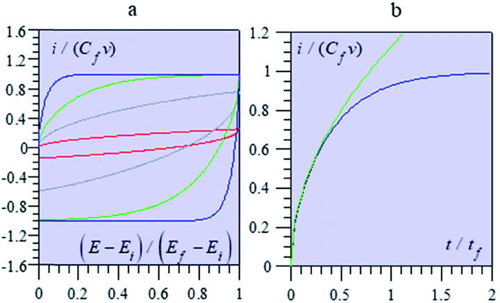 | ||
| Fig. 13 Variation of the dimensionless current function with (a) the dimensionless potential, (E − Ei)/(Ef − Ei) for several values of the parameter tf/tv = 0.1 (blue), 0.5 (green), 2 (grey), and 20 (red), with negligible solution resistance Ru = 0; (b) with the dimensionless time t/tf, with tf/tv = 0.5 and Ru = 0 (blue line). The green line is the limiting behaviour observed at short times. | ||
 | ||
| Fig. 14 Variations of the capacitance with scan rate from MnO2 electrodes in ref. 69 (from multicycle limiting CV responses). (a) Amorphous, (b) birnessite, (c) spinel, in aqueous Li2SO4 (red) and (NMe4)2SO4 (blue). Data points: closed circles. Full lines: fitting of data by means of a transmission line model. Dotted lines: simulations with a RC model (see ref. 68 for details). | ||
It is remarkable that the short time behaviour is a square root dependence, reminiscent of diffusion. Actually, the potential in the pore obeys the second Fick's law, which governs matter diffusion as well, but also heat transfer. This is purely coincidental and should not create confusion about the actual mechanism of charging dynamics.68
Provision has been made to treat the cases where resistance in the solution outside the pores is not negligible.68 We also note that Fig. 13 deals with first cycle CV responses. Upon repeating the potential cycles, the responses tend asymptotically toward a limit. These multicycling responses are often those that are available in literature data, as will be seen next. Their theoretical derivation has also been treated.68
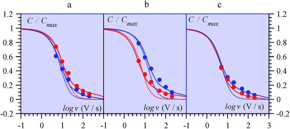
Ref. 69 offers an interesting set of experimental CV capacitive responses for three types of MnO2 electrode coating, where the effect of scan rate was systematically investigated (Fig. 14). These results were originally presented under the “pseudocapacitance” flag and the observed variations of the capacitance with the scan rate, thought to derive from coupled counter-ion diffusion.
As detailed in the present work, such “pseudocapacitive” responses should instead be viewed as truly capacitive and giving the opportunity to test the applicability of the pore ohmic drop model developed earlier. It can indeed be seen in Fig. 14 that the fitting of the experimental data by the predictions of the transmission line model is quite satisfactory.
This is also the occasion to mention analyses of such data in the framework of counter-ion diffusion where the variations of the current, I, with the scan rate, ν, are based on the two following equations,70 or their equivalent in terms of capacitance,69
| I = aνb and/or I = k1ν + k2ν1/2 |
These two equations are incompatible with each other and have no kind of justification. Their application has clearly no bearings and should therefore be avoided.
7. Conclusions and prospects
In summary, if one sticks to the rigorous definition of “pseudocapacitive” materials as having the electrochemical signature of a capacitance, while being derived from the superposition of closely spaced faradaic couples, it must be concluded that such items are fictional. In the potential domain where they show a capacitive response, they simply behave as electronic conductors forming an electrical double layer at the contact with the bathing ionic solution. This implies that, starting from an insulating state, faradaic reactions are at work in the building of the conduction bands involved in the ohmic conduction potential domains.In these domains, the performances of the so called “pseudocapacitive” materials are to be judged on the same grounds as for the classical double layer charging devices. Strategies to improve them are based on a better comprehension of their relationship with the material structure. This involved the optimization of the capacitance but also the time response of the charging process, so as to improve not only the stored energy but also power of the energy storage device. This last issue and notably its relationship with the structure of porous materials certainly deserve a reinforced scrutiny.
Conflicts of interest
There are no conflicts to declare.References
- M. Winter and R. J. Brodd, Chem. Rev., 2004, 104, 4245–4269 CrossRef CAS PubMed.
- Note that in some cases, the species that cross the interfacial potential drop is an ion rather than an electron. See for example: H. S. White, J. D. Peterson, Q. Cui and K. J. Stevenson, J. Phys. Chem. B, 1998, 102, 2930–2934 CrossRef CAS.
- Note that we use here the term ‘double layer’ for electrochemical capacitive processes although the classical Gouy–Chapman–Stern double layer model (see ref. 4) applies for planar electrodes. More complex models may have to be considered for porous electrodes.
- P. Delahay, Double Layer and Electrode Kinetics, Wiley, New York, 1955, ch. 7 Search PubMed.
- J.-M. Savéant, Elements of molecular and biomolecular electrochemistry: an electrochemical approach to electron transfer chemistry, John Wiley & Sons, Hoboken, NJ, 2006 Search PubMed.
- (a) E. Laviron, Bull. Soc. Chim. Fr., 1967, 3717–3721 CAS; (b) E. Laviron, Voltammetric Method for the Study of Adsorbed Species, in Electroanalytical Chemistry, ed. A. J. Bard, Dekker, New York, 1982, vol. 12 Search PubMed.
- (a) J. E. B. Randles, Trans. Faraday Soc., 1948, 44, 327–338 RSC; (b) A. Sevcik, Collect. Czech. Chem. Commun., 1948, 13, 349–377 CrossRef CAS; (c) H. Matsuda and Y. Ayabe, Z. Elektrochem., 1955, 59, 494–503 CAS.
- (a) B. E. Conway and E. Gileadi, Trans. Faraday Soc., 1962, 58, 2493–2509 RSC; (b) B. E. Conway, J. Electrochem. Soc., 1991, 138, 1539–1548 CrossRef CAS; (c) B. E. Conway, V. Birss and J. Wojtowicz, J. Power Sources, 1997, 66, 1–14 CrossRef CAS.
- T. Brousse, D. Belanger and J. W. Long, J. Electrochem. Soc., 2015, 162, A5185–A5189 CrossRef CAS.
- B. E. Conway, Electrochemical Supercapacitors: Scientific Fundamentals and Technological Applications, Kluwer Academic/Plenum, New York, 1999 Search PubMed.
- C. Costentin, T. R. Porter and J.-M. Savéant, ACS Appl. Mater. Interfaces, 2017, 9, 8649–8658 CrossRef CAS PubMed.
- P. Simon and Y. Gogotsi, Nat. Mater., 2008, 7, 845–854 CrossRef CAS PubMed.
- A. Eftekhari and M. Mohamedi, Materials Today Energy, 2017, 6, 211–229 CrossRef.
- P. Guillemet, T. Brousse, O. Crosnier, Y. Dandeville, L. Athouel and Y. Scudeller, Electrochim. Acta, 2012, 67, 41–49 CrossRef CAS.
- M. W. Kanan, Y. Surendranath and D. G. Nocera, Chem. Soc. Rev., 2009, 38, 109–114 RSC.
- D. G. Nocera, Acc. Chem. Res., 2012, 45, 767–776 CrossRef CAS PubMed.
- D. K. Bediako, A. M. Ullman and D. G. Nocera, Top. Curr. Chem., 2016, 371, 173–214 CrossRef CAS PubMed.
- C. Costentin, T. R. Porter and J.-M. Savéant, J. Am. Chem. Soc., 2016, 138, 5615–5622 CrossRef CAS.
- C. Costentin, T. R. Porter and J.-M. Savéant, submitted.
- J. Bisquert, Nanostructured Energy Devices. Equilibrium Concepts and Kinetics, CRC Press, 2015, ch. 8 and 9 Search PubMed.
- (a) J. Bisquert and A. Zaban, Appl. Phys. A, 2003, 77, 507–565 CrossRef CAS; (b) F. Fabregat-Santiago, I. Mora-Seró, G. Garcia-Belmonte and J. Bisquert, J. Phys. Chem. B, 2003, 107, 758–768 CrossRef CAS.
- S. Trasatti and G. Buzzanca, J. Electroanal. Chem., 1971, 29, A1–A5 CrossRef.
- S. Hadzi-Jordanov, H. Angerstein-Kozlowska, M. Vukovič and B. E. Conway, J. Electrochem. Soc., 1978, 125, 1471–1480 CrossRef CAS.
- T. R. Jow and J. P. Zheng, J. Electrochem. Soc., 1998, 145, 49–52 CrossRef CAS.
- C. C. Hu and Y. H. Huang, J. Electrochem. Soc., 1999, 146, 2465–2471 CrossRef CAS.
- (a) Y. Mo, M. R. Antonio and D. A. Scherson, J. Phys. Chem. B, 2000, 104, 9777–9779 CrossRef CAS; (b) I. C. Stefan, Y. Mo, M. R. Antonio and D. A. Scherson, J. Phys. Chem. B, 2002, 106, 12373–12375 CrossRef CAS.
- J. M. Fletcher, W. E. Gardner, B. F. Greenfield, M. J. Holdoway and M. H. Rand, J. Chem. Soc. A, 1968, 653–657 RSC.
- W. Dmowski, T. Egami, K. E. Swider-Lyons, C. T. Love and D. R. Rolison, J. Phys. Chem. B, 2002, 106, 12677–12683 CrossRef CAS.
- K. H. Chang and C. C. Hu, J. Electrochem. Soc., 2004, 151, A958–A964 CrossRef CAS.
- S. Sopčić, Z. Mandić, G. Inzelt, M. K. Roković and E. Meštrović, J. Power Sources, 2011, 196, 4849–4858 CrossRef.
- J. B. Mitchell, W. C. Lo, A. Genc, J. LeBeau and V. Augustyn, Chem. Mater., 2017, 29, 3928–3937 CrossRef CAS.
- N. Yoshida, Y. Yamada, S.-i. Nishimura, Y. Oba, M. Ohnuma and A. Yamada, J. Phys. Chem. C, 2013, 117, 12003–12009 CrossRef CAS.
- (a) W. Sugimoto, K. Yokoshima, Y. Murakami and Y. Takasu, Electrochim. Acta, 2006, 52, 1742–1748 CrossRef CAS; (b) W. Sugimoto, H. Iwata, K. Yokoshima, Y. Murakami and Y. Takasu, J. Phys. Chem. B, 2005, 109, 7330–7338 CrossRef CAS.
- V. Ozoliņš, F. Zhou and M. Asta, Acc. Chem. Res., 2013, 46, 1084–1093 CrossRef.
- H. Y. Lee and J. B. Goodenough, J. Solid State Chem., 1999, 144, 220–223 CrossRef CAS.
- A. Kozawa and R. A. Powers, J. Electrochem. Soc., 1966, 113, 870–878 CrossRef CAS.
- (a) S. Devaraj and N. Munichandraiah, J. Phys. Chem. C, 2008, 112, 4406–4417 CrossRef CAS; (b) O. Ghodbane, F. Ataherian, N.-L. Wu and F. Favier, J. Power Sources, 2012, 206, 454–462 CrossRef CAS; (c) A. Boisset, L. Athouël, J. Jacquemin, P. Porion, T. Brousse and M. Anouti, J. Phys. Chem. C, 2013, 117, 7408–7422 CrossRef CAS; (d) Y. Q. Li, X. M. Shi, X. Y. Lang, Z. Wen, J. C. Li and Q. Jiang, Adv. Funct. Mater., 2016, 26, 1830–1839 CrossRef CAS.
- O. Ghodbane, J.-L. Pascal and F. Favier, ACS Appl. Mater. Interfaces, 2009, 1, 1130–1139 CrossRef CAS.
- S. L. Kuo and N. L. Wu, J. Electrochem. Soc., 2006, 153, A1317–A1324 CrossRef CAS.
- D. Chen, W. Pan and D. Xue, J. Phys. Chem. C, 2016, 120, 20077–20081 CrossRef.
- D. Chen, D. Ding, X. Li, G. H. Waller, X. Xiong, M. A. El-Sayed and M. Liu, Chem. Mater., 2015, 27, 6608–6619 CrossRef CAS.
- J. Wang and A. J. Bard, J. Am. Chem. Soc., 2001, 123, 498–499 CrossRef CAS.
- M. Toupin, T. Brousse and D. Bélanger, Chem. Mater., 2004, 16, 3184–3190 CrossRef CAS.
- J.-K. Chang, M.-T. Lee and W.-T. Tsai, J. Power Sources, 2007, 166, 590–594 CrossRef CAS.
- K.-W. Nam, M. G. Kim and K.-B. Kim, J. Phys. Chem. C, 2007, 111, 749–758 CrossRef CAS.
- H.-W. Chang, Y.-R. Lu, J.-L. Chen, C.-L. Chen, J.-F. Lee, J.-M. Chen, Y.-C. Tsai, P.-H. Yeh, W. C. Chou and C.-L. Dong, Phys. Chem. Chem. Phys., 2016, 18, 18705–18718 RSC.
- Y. P. Zhu, C. Xia, Y. J. Lei, N. Singh, U. Schwingenschlogl and H. N. Alshareef, Nano Energy, 2019, 56, 357–364 CrossRef CAS.
- Y. Bai, I. Mora-Seró, F. De Angelis, J. Bisquert and P. Wang, Chem. Rev., 2014, 114, 10095–10130 CrossRef CAS PubMed.
- F. Fabregat-Santiago, H. Randriamahazaka, A. Zaban, J. Garcia-Canadas, G. Garcia-Belmonte and J. Bisquert, Phys. Chem. Chem. Phys., 2006, 8, 1827–1833 RSC.
- I. Abayev, A. Zaban, F. Fabregat-Santiago and J. Bisquert, Phys. Status Solidi A, 2003, 196, R4–R6 CrossRef CAS.
- (a) C. N. Brodsky, D. K. Bediako, C. Shi, T. P. Keane, C. Costentin, S. J. L. Billinge and D. G. Nocera, ACS Appl. Energy Mater., 2019, 2, 3–12 CrossRef CAS; (b) C. Costentin and D. G. Nocera, J. Phys. Chem. C, 2019, 123, 1966–1973 CrossRef CAS.
- (a) Y.-S. Kim, S. Kriegel, K. D. Harris, C. Costentin, B. Limoges and V. Balland, J. Phys. Chem. C, 2017, 121, 10325–10335 CrossRef CAS; (b) Y. S. Kim, V. Balland, B. Limoges and C. Costentin, Phys. Chem. Chem. Phys., 2017, 19, 17944–17951 RSC.
- (a) B. Reichman and A. J. Bard, J. Electrochem. Soc., 1980, 127, 241–242 CrossRef CAS; (b) B. Reichman and A. J. Bard, J. Electrochem. Soc., 1981, 128, 344–346 CrossRef CAS.
- J. W. Kim, V. Augustyn and B. Dunn, Adv. Energy Mater., 2012, 2, 141–148 CrossRef CAS.
- K. Brezesinski, J. Wang, J. Haetge, C. Reitz, S. O. Steinmueller, S. H. Tolbert, B. M. Smarsly, B. Dunn and T. Brezesinski, J. Am. Chem. Soc., 2010, 132, 6982–6990 CrossRef CAS PubMed.
- V. Augustyn, J. Come, M. A. Lowe, J. W. Kim, P.-L. Taberna, S. H. Tolbert, H. D. Abruña, P. Simon and B. Dunn, Nat. Mater., 2013, 12, 518 CrossRef CAS.
- J. Come, V. Augustyn, J. W. Kim, P. Rozier, P.-L. Taberna, P. Gogotsi, J. W. Long, B. Dunn and P. Simon, J. Electrochem. Soc., 2014, 161, A718–A725 CrossRef CAS.
- D. Chen, J.-H. Wang, T.-F. Chou, B. Zhao, M. A. El-Sayed and M. Liu, J. Am. Chem. Soc., 2017, 139, 7071–7081 CrossRef CAS.
- (a) V. Nicolosi, M. Chhowalla, M. G. Kanatzidis, M. S. Strano and J. N. Coleman, Science, 2013, 340, 1226419 CrossRef; (b) E. Pomerantseva and Y. Gogotsi, Nat. Energy, 2017, 2, 6 Search PubMed.
- B. Anasori, M. R. Lukatskaya and Y. Gogotsi, Nat. Rev. Mater., 2017, 2, 16098 CrossRef CAS.
- M. R. Lukatskaya, O. Mashtalir, C. E. Ren, Y. Dall'Agnese, P. Rozier, P. L. Taberna, M. Naguib, P. Simon, M. W. Barsoum and Y. Gogotsi, Science, 2013, 341, 1502–1505 CrossRef CAS.
- M. R. Lukatskaya, S. Kota, Z. F. Lin, M. Q. Zhao, N. Shpigel, M. D. Levi, J. Halim, P. L. Taberna, M. Barsoum, P. Simon and Y. Gogotsi, Nat. Energy, 2017, 2, 17105 CrossRef CAS.
- M. D. Levi, M. R. Lukatskaya, S. Sigalov, M. Beidaghi, N. Shpigel, L. Daikhin, D. Aurbach, M. W. Barsoum and Y. Gogotsi, Adv. Energy Mater., 2015, 5, 1400815 CrossRef.
- M. R. Lukatskaya, S. M. Bak, X. Q. Yu, X. Q. Yang, M. W. Barsoum and Y. Gogotsi, Adv. Energy Mater., 2015, 5, 1500589 CrossRef.
- M. Okubo, A. Sugahara, S. Kajiyama and A. Yamada, Acc. Chem. Res., 2018, 51, 591–599 CrossRef CAS.
- J. Huang, B. G. Sumpter and V. Meunier, Angew. Chem., Int. Ed. Engl., 2008, 47, 520–524 CrossRef CAS.
- A. A. Kornyshev and R. Qiao, J. Phys. Chem. C, 2014, 118, 18285–18290 CrossRef CAS.
- C. Costentin and J.-M. Savéant, submitted.
- L. Coustan, P. Lannelongue, P. Arcidiacono and F. Favier, Electrochim. Acta, 2016, 206, 479–489 CrossRef CAS.
- M. Forghani and S. W. Donne, J. Electrochem. Soc., 2018, 165, A664–A673 CrossRef CAS.
Footnotes |
| † Electronic supplementary information (ESI) available. See DOI: 10.1039/c9sc01662g |
| ‡ Present address: Department of Chemistry and Chemical Biology, Harvard University, 12 Oxford Street, Cambridge, Massachusetts 02138, USA. |
| This journal is © The Royal Society of Chemistry 2019 |