
 Open Access Article
 This Open Access Article is licensed under a Creative Commons Attribution-Non Commercial 3.0 Unported Licence
All-inorganic quantum dot assisted enhanced charge extraction across the interfaces of bulk organo-halide perovskites for efficient and stable pin-hole free perovskite solar cells†
Dibyendu
Ghosh‡
 a,
Dhirendra K.
Chaudhary‡
a,
Md. Yusuf
Ali
a,
Kamlesh Kumar
Chauhan
b,
Sayan
Prodhan
c,
Sayantan
Bhattacharya
c,
Barun
Ghosh
d,
P. K.
Datta
c,
Sekhar C.
Ray
d and
Sayan
Bhattacharyya
*a
a,
Dhirendra K.
Chaudhary‡
a,
Md. Yusuf
Ali
a,
Kamlesh Kumar
Chauhan
b,
Sayan
Prodhan
c,
Sayantan
Bhattacharya
c,
Barun
Ghosh
d,
P. K.
Datta
c,
Sekhar C.
Ray
d and
Sayan
Bhattacharyya
*a
aDepartment of Chemical Sciences, Centre for Advanced Functional Materials, Indian Institute of Science Education and Research (IISER) Kolkata, Mohanpur 741246, India. E-mail: sayanb@iiserkol.ac.in
bDepartment of Electrical Engineering, Indian Institute of Technology (IIT) Kharagpur, Kharagpur – 721302, India
cDepartment of Physics, Indian Institute of Technology (IIT) Kharagpur, Kharagpur – 721302, India
dDepartment of Physics, CSET, University of South Africa, Private Bag X6, Florida, 1710, Science Campus, Christiaan de Wet and Pioneer Avenue, Florida Park, Johannesburg, South Africa
First published on 23rd August 2019
Abstract
In spite of achieving high power conversion efficiency (PCE), organo-halide perovskites suffer from long term stability issues. Especially the grain boundaries of polycrystalline perovskite films are considered as giant trapping sites for photo-generated carriers and therefore play an important role in charge transportation dynamics. Surface engineering via grain boundary modification is the most promising way to resolve this issue. A unique antisolvent-cum-quantum dot (QD) assisted grain boundary modification approach has been employed for creating monolithically grained, pin-hole free perovskite films, wherein the choice of all-inorganic CsPbBrxI3−x (x = 1–2) QDs is significant. The grain boundary filling by QDs facilitates the formation of compact films with 1–2 μm perovskite grains as compared to 300–500 nm grains in the unmodified films. The solar cells fabricated by CsPbBr1.5I1.5 QD modification yield a PCE of ∼16.5% as compared to ∼13% for the unmodified devices. X-ray photoelectron spectral analyses reveal that the sharing of electrons between the PbI6− framework in the bulk perovskite and Br− ions in CsPbBr1.5I1.5 QDs facilitates the charge transfer process while femtosecond transient absorption spectroscopy (fs-TAS) suggests quicker trap filling and enhanced charge carrier recombination lifetime. Considerable ambient stability up to ∼720 h with <20% PCE degradation firmly establishes the strategic QD modification of bulk perovskite films.
Introduction
In recent years, organic–inorganic hybrid perovskites especially CH3NH3PbI3 have attracted unprecedented attention from the scientific community as a photoactive layer in low-cost photovoltaic (PV) devices.1,2 This interesting class of materials exhibits profitable optoelectronic properties such as high absorption coefficients, long electron–hole diffusion lengths, ambipolar charge transport and wide range tunability of the optical band gap.3 Together they have assisted in achieving the increase of power conversion efficiency (PCE) of perovskite solar cells up to a record 23.3%.4 However their commercial success remains elusive because of the limitations in long term device stability under ambient operation conditions, and due to the presence of hysteresis in the current–voltage characteristics and lower efficiencies in large area cells, which pose major challenges for practical PV applications. Both the PCE and stability of perovskite solar cell devices concomitantly depend on multiple factors such as device architecture, perovskite composition, electron and hole transport layers (ETL and HTL) and most importantly the nature of surfaces and interfaces.5–7The perovskite film surface and its interface with the ETL and HTL modulate the solar cell performance through the extraction and transport of photogenerated charge carriers with the purpose of minimum electron–hole recombination. In polycrystalline perovskite films, the grain boundaries separating differently oriented crystalline grains create insulating interlayers that severely impact this charge transportation dynamics.8 Moreover, the nonstoichiometric crystals or impurities at the grain boundaries forge defect states that result in unbalanced charge accumulation or trapping. The immediate solution is to improve the grain size by engineering the inter-grain interface. One of the most favoured propositions is the Lewis acid–base adduct approach to form compact large grains for high efficiency perovskite solar cells where the Pb(II) halides that serve as Lewis acids and oxygen donors (dimethyl sulfoxide/DMSO, N,N-dimethylformamide/DMF, and N-methyl-2-pyrrolidone/NMP), sulfur donors (thiourea and thioacetamide), and nitrogen donors (pyridine and aniline) are Lewis bases.9 DMSO and DMF help to form compact grains via formation of MAI·PbI2·DMSO and MAI·PbI2·DMF immediate phases, respectively by donating a pair of electrons to form Lewis adducts with Pb2+ which controls the fast reaction kinetics between PbI2 and organic iodide in solution.10–12 However a weak coordination between Pb2+ and O2− leads to easy escape of the oxygen donor from the PbI2 framework causing insufficient perovskite grain growth and formation of a large number of trap states.13
Among the post-treatment techniques, antisolvent showers with toluene, chlorobenzene, diethyl ether, ethyl acetate, etc. have been widely accepted as a route to grow uniform perovskite thin films since the antisolvent can accelerate heterogeneous nucleation through instantaneous local supersaturation on the spinning substrate.10,14,15 But the rapid crystallization during antisolvent treatment ends up creating pin-holes leading to ion migration channels. Since the electric field at the ETL/perovskite and perovskite/HTL interfaces is not strong enough for efficient electron or hole extraction,16 electrons and holes accumulate at these interfaces, which is responsible for the hysteresis behaviour and irreversible degradation.17 Several modifications have been adopted to minimize the surface defect states and to ensure fast charge extraction across these interfaces.18,19 For instance, benzenethiol modification at the perovskite/HTL interface facilitates fast hole transfer,19 an organic π-conjugated Lewis base interlayer between the ETL and perovskite passivates trap states for effective charge extraction,20 and paired electric dipole layers can adjust the surface potential for rapid charge carrier separation.21 However, most of the above strategies end up creating more heterostructured interfaces resulting in additional trap states, further limited by the small device area (<0.1 cm2).
To address the above gap areas, we have introduced a dual strategy of antisolvent cum QD modification for achieving monolithically grained bulk CH3NH3PbI3−xClx perovskite films where all the inorganic CsPbBrxI3−x (x = 1–2) QDs are dispersed in an antisolvent (here chlorobenzene, CB) which primarily fills the grain boundaries of bulk perovskite film. The antisolvent increases the grain size by rapid crystallization because of which the QDs can fill the pin-holes, thereby passivating the surface trap states. Due to the isotropic crystal structure of the QDs and bulk, electron conduction channels are facilitated for better transport of charge carriers with improved recombination time. Among the other QD compositional variations, a favourable band position and compositional stability of CsPbBr1.5I1.5 QDs help in achieving a PCE of ∼16.5% and an ambient durability of ∼720 h for CsPbBr1.5I1.5 QD modified devices of ∼0.1 cm2 area. However, the PCE decreases to ∼13% for PV devices having a larger area of 1 cm2. The mechanistic consequences are systematically studied by ultraviolet and X-ray photoelectron spectroscopic techniques (UPS and XPS) and fs-TAS. It is worthy of note that our approach of grain boundary modification by QDs greatly differs from the tandem device architectures where the QD layer is used as a secondary absorber along with the bulk perovskite.22
Results and discussion
The preparation method of the bulk perovskite CH3NH3PbI3−xClx absorber layer and the change in surface topology after antisolvent treatment and QD modification are schematically shown in Fig. 1a–c. After depositing the bulk perovskite film onto a mesoporous TiO2 layer by spin coating, the QD dispersion in anhydrous CB was spin coated in the second step to prepare the QD modified perovskite films (Experimental section). To achieve a near-perfect passivation of the defect states, the QD deposited films were dipped 2 times each for 2 s in a methyl acetate solution of lead nitrate in order to remove the ligands from the QD surface. The successful ligand removal is evident from the Fourier-transform infrared (FTIR) spectra in Fig. S1,† where after treatment, the vibrational bands at 500–2000 cm−1, due to the C–H modes of the organic ligands are found to be negligible. Three different halide compositions are chosen for the perovskite QDs viz. CsPbBr3, CsPbBr1.5I1.5 and CsPbBrI2 with an average cuboid size of ∼10 nm (Fig. S2a–c†) and a perfect cubic crystal structure (Fig. S2d†). All three QDs demonstrate absorption and emission bands in the visible region whereby increasing the Br/I ratio results in a blue shift (Fig. S2e and f†). As observed from the surface morphology of the films in Fig. 1d–f, the grain size increases from 300–500 nm in the unmodified film to 1–2 μm after CB and QD modifications. Although the antisolvent assisted fast crystallization allows formation of bigger grains,14 the CB modified films still contain voids and pin-holes at the intra-grain interfaces. In contrast, the CsPbBr1.5I1.5 QD modified film shows monolithically grained and pin-hole free compact films (Fig. 1f) mainly due to in situ filling of the QDs in the voids as well as grain boundaries. Since the long chain organic ligands are removed post deposition, the QD filled pin-holes remain free of these ligands. The wettability of the films was tested and it was found that the contact angle increases with CB and QD surface modifications (inset of Fig. 1d–f). Such exceptional improvement in the film morphology is also observed with CsPbBr3 and CsPbBrI2 QDs (Fig. S3†). The atomic force microscope (AFM) images (Fig. S4†) corroborate the above observations. The average surface roughness improves from ∼350 nm for the unmodified films to ∼70 nm for the CsPbBr1.5I1.5 QD modified films, which is similar to the improvements in CsPbBr3 and CsPbBrI2 QD modified perovskite films (Fig. S5†).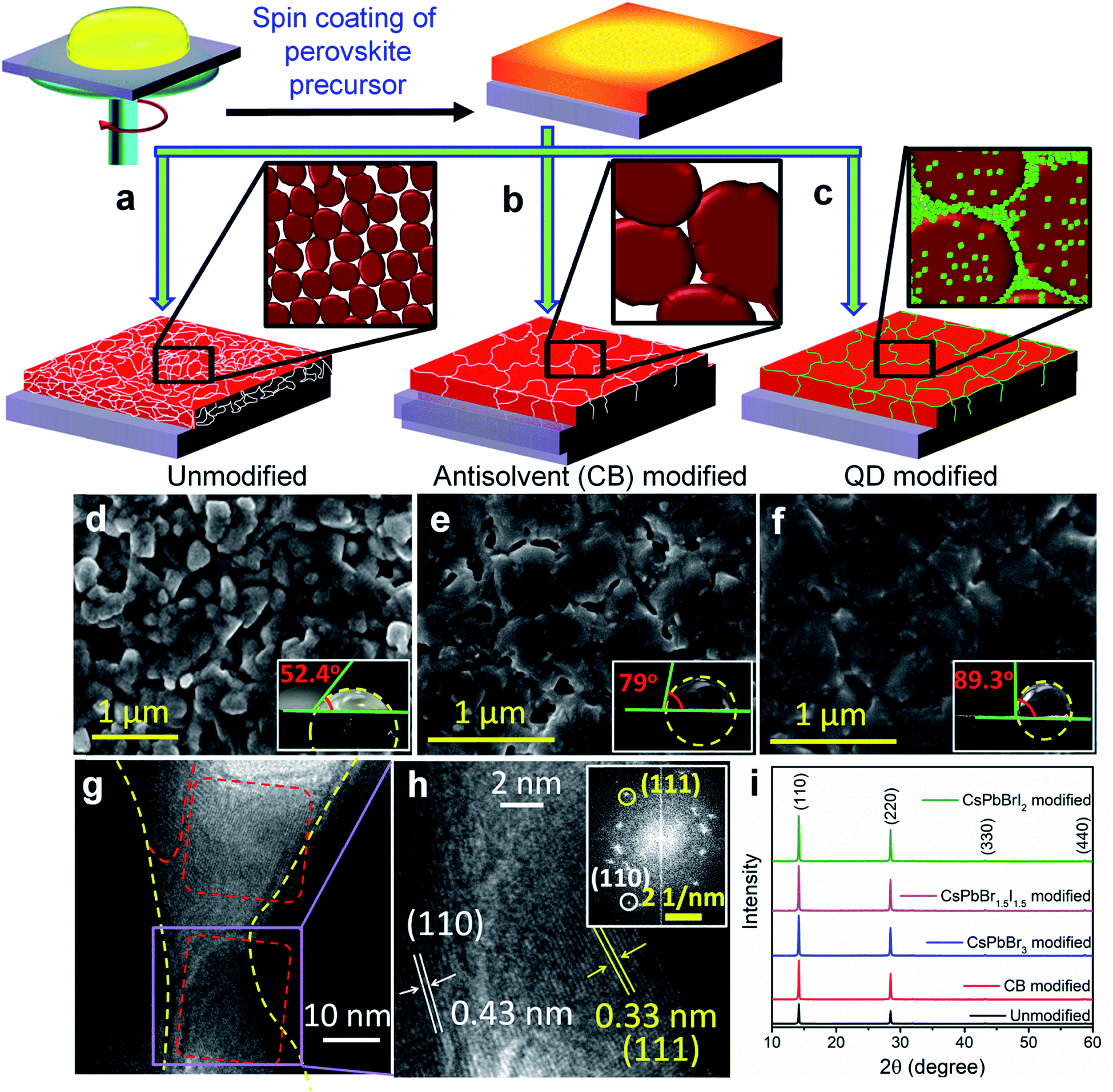 | ||
| Fig. 1 Schematic representation of the growth procedure of the (a) unmodified, (b) CB-modified and (c) CsPbBr1.5I1.5 QD (green dots) modified bulk perovskite thin films. Insets show the schematics of morphological evolution. Field emission scanning electron microscope (FE-SEM) images and insets showing the corresponding contact angles of the (d) unmodified, (e) CB-modified and (f) CsPbBr1.5I1.5 QD modified perovskite thin films. (g) HR-TEM image of the CsPbBr1.5I1.5 QD modified perovskite and (h) selected area magnified view with the inset showing the SAED pattern from the magnified portion. (i) XRD patterns of the unmodified, CB-modified and three types of QD [CsPbBr3, CsPbBr1.5I1.5, and CsPbBrI2] modified perovskite films. | ||
To gain deeper insights into the perovskite grains, high resolution transmission electron microscopy (HR-TEM) analysis was performed near the grain boundaries of the representative CsPbBr1.5I1.5 QD modified films and the results show that the QDs fill the voids and interconnect the bulk perovskite grains (Fig. 1g). In the magnified view, separate interplanar spacings of 0.43 nm corresponding to the (110) reflection of bulk CH3NH3PbI3−xClx and 0.33 nm corresponding to the (111) plane of the CsPbBr1.5I1.5 QDs can be vividly observed (Fig. 1h). In addition, the reciprocal lattice points from both bulk CH3NH3PbI3−xClx and CsPbBr1.5I1.5 QDs are observed in the selected area electron diffraction (SAED) pattern in Fig. 1h (inset). Elemental mapping on the high-angle annular dark-field scanning TEM (HAADF-STEM) image further confirms the filling of pinholes by these QDs (Fig. S6†). The X-ray diffraction (XRD) patterns of the modified and unmodified perovskite films (Fig. 1i) indicate reflections at 2θ = 14.14, 28.44, 43.24 and 58.95° corresponding respectively to the (110), (220), (330) and (440) planes of tetragonal CH3NH3PbI3.1,23 The Scherrer equation helps in extracting the crystallite size of the coherently diffracting domains from the highest intensity (110) reflection.24 Table S1† shows the increase in crystalline domain size with anti-solvent and QD modified films, which further manifests the increase in grain size as also observed from Fig. 1d–f. In the UV-vis absorption spectra (Fig. S7†), there is a negligible change in the absorption onset of the differently modified films (Table S1†). An increase in absorbance and a reduction in the Urbach tail are observed for the CsPbBr1.5I1.5 and CsPbBrI2 QD modified films primarily because of the passivation of trap states (ESI discussion†),25 which also results in a blue shift of the emission maxima. To understand the surface positioning of the QDs, elemental line scans were performed at multiple grain boundaries of the CsPbBr1.5I1.5 QD modified perovskite films (Fig. S8a†). Besides the QD distribution on top of the perovskite grains, a predominant grain boundary filling by the QDs is evident from the higher counts of Cs and Br in between the grains, whereas Pb and I counts remain almost constant. Grazing incidence XRD (GI-XRD) performed at different GI angles was used to probe the possibility of crystal phase modifications at different depths from the top surface of the CsPbBr1.5I1.5 QD modified bulk film (Fig. S8b†). At a very low GI angle (0.05°), only the peaks due to CsPbBr1.5I1.5 QDs could be observed but with increasing GI angle the peaks due to bulk CH3NH3PbI3−xClx (MAPbI3−xClx) start appearing without any change in peak position which otherwise could have been shifted by formation of a mixed cation perovskite such as CsyMA1−yPbI3−xClx. Therefore, it can be inferred that the QDs only act as pin-hole fillers without changing the crystal structure of the bulk perovskite.
PV devices were fabricated separately with the unmodified, CB modified and QD modified perovskite films according to the device architecture shown in Fig. 2a. The cross-sectional FE-SEM image of a representative CsPbBr1.5I1.5 QD modified device is shown in Fig. 2b. The thickness of the QD modified compact perovskite layer is 400–450 nm. The corresponding energy level (derived from UPS analyses discussed later) diagram along with charge transport mechanism is shown in Fig. 2c. The concentration of QDs in CB is first optimized to 10 mg ml−1 for all three halide compositions (Fig. S9 and Table S2†) and thereafter the same concentration is used for comparative analysis. Fig. 2d shows the J–V characteristics of the unmodified, and CB and QD modified devices under 1 sun illumination and the parameters are tabulated in Table 1. The device efficiency improves significantly after QD modification of the films. The unmodified devices show a PCE (η) of 12.9% while the PCE of the CB, CsPbBr3, CsPbBr1.5I1.5 and CsPbBrI2 modified devices is 14.1, 11.2, 16.5 and 16.7%, respectively. Although all the QDs can fill pin-holes thereby providing a compact perovskite layer, the lower PCE with CsPbBr3 QDs is due to their unfavorable band position (validated from UPS measurements, discussed later). This fact is also indicated from less PL quenching at the CH3NH3PbI3−xClx/CsPbBr3 QD modified films (Fig. S7b†) than at the CsPbBr1.5I1.5 and CsPbBrI2 QD modified perovskite films. At least 100 devices were measured to check the reproducibility of the PCE of the devices with the unmodified, and CB and CsPbBr1.5I1.5 QD modified films (Fig. S10†). The devices with the unmodified perovskite film show a wide PCE distribution due to a large variation in surface morphology and randomly scattered voids while an almost uniform morphology of QD modified films in every batch of fabricated devices yields excellent reproducibility in device efficiency. To obtain further insight into the effect of QD modification, external quantum efficiency (EQE) spectra of the solar cells were recorded (Fig. 2e) and they show a flat region in the spectral range of 450–700 nm with an EQE of ∼88%. The associated integrated short circuit current density calculated from the EQE is in close proximity to the JSC values obtained from J–V plots. CsPbBr1.5I1.5 QD modification even minimizes the hysteresis in forward and reverse potential scan directions in the J–V plot to almost negligible, which otherwise is quite significant (Fig. S11†). QD modification quite successfully eliminates the processes of dynamic trapping and detrapping of electrons/holes, which are a major drawback in conventional hybrid perovskite solar cells.26 In QD modified films with larger grains, the grain boundaries are reduced, which allows passivation of trap levels, thus minimizing the annihilation of photogenerated carriers. Also, since QD modification assists in favorable energy band alignment, encouraging balanced charge transfer (discussed later), it prevents the creation of capacitive elements from minimally accumulated asymmetric charge carriers. In addition, near-depletion of the TiO2/perovskite interface helps in suppressing the effect of trap levels within TiO2 layers. These factors curtail the migration of cations and their accumulation near the interfaces in the form of space charge, resulting in negligible hysteresis. Due to negligible hysteresis in the J–V plot, the current density remains independent of the voltage scan rate (Fig. S11b†). In order to generalize our approach, the concept of QD modification was also applied to the triple cation perovskite Cs0.05(MA0.17FA0.83)0.95Pb(I0.83Br0.17)3. Here too, the PCE improves from 17.2 to 19.4% after modification with CsPbBr1.5I1.5 QDs (Fig. S12a†). The film topology before and after QD treatment also validates the removal of pin-holes in the triple cation perovskite film (Fig. S12b and c†).
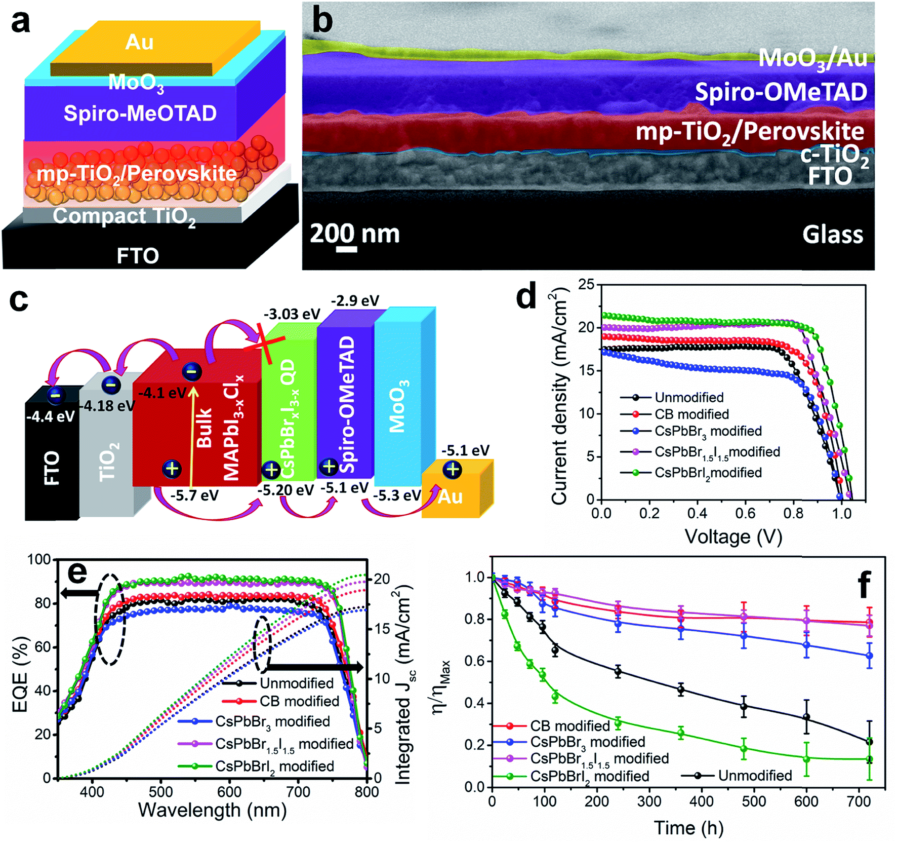 | ||
| Fig. 2 (a) Schematic layered configuration, (b) cross-sectional FE-SEM image, and (c) energy level diagram along with the charge transport mechanism of the PV devices. (d) J–V characteristics of the unmodified, CB modified and QD modified devices. (e) EQE and integrated JSC plots for the unmodified, CB modified and QD modified devices. (f) 720 h of PCE stability of the unmodified, CB-modified and QD modified devices measured according to ISOS-D1 protocols. | ||
| Samples | V OC (V) | J SC (mA cm−2) | Fill factor | Efficiency (%) | R rec (Ω) | V bi (V) | W L (nm) |
|---|---|---|---|---|---|---|---|
| Unmodified | 0.995 | 17.43 | 0.74 | 12.90 ± 0.80 | 869 | 0.93 | 56.75 |
| CB modified | 1.01 | 18.98 | 0.73 | 14.07 ± 0.50 | 1662 | 0.96 | 93.85 |
| CsPbBr3 modified | 0.996 | 17.18 | 0.65 | 11.22 ± 0.40 | 8472 | 0.91 | 99.52 |
| CsPbBr1.5I1.5 modified | 1.03 | 20.02 | 0.79 | 16.51 ± 0.20 | 10![[thin space (1/6-em)]](https://www.rsc.org/images/entities/char_2009.gif) 102 102 |
1.01 | 156.24 |
| CsPbBrI2 modified | 1.03 | 21.35 | 0.76 | 16.71 ± 0.18 | 6851 | 1.00 | 111.72 |
To investigate the shelf-life of the devices, degradation studies were performed following the protocols of the International Summit on Organic Photovoltaic Stability (ISOS)-D1.27 According to this protocol, devices are stored in the dark under ambient conditions (temperature 24 °C ± 3 °C and relative humidity 44 ± 6%) and measurements are performed on the devices periodically under simulated solar light. Fig. 2f shows the normalized degradation profile of the PCE of the unencapsulated devices while the rest of the device parameters (JSC, VOC and FF) are shown in Fig. S13.† The unmodified and CsPbBrI2 QD modified devices lose 20% device efficiency within the first 40 h. The grain boundaries in the bulk perovskite consist of an amorphous intergranular layer which allows fast moisture diffusion,28 the case encountered in the unmodified perovskite film. The presence of pin-holes also provides appropriate pathway for moisture percolation within the intergranular interface. In the CsPbBr3 and CsPbBr1.5I1.5 QD modified devices, the formation of pin-hole free larger grains and the depletion of grain boundary fractions by the QD interlayer make them moisture tolerant. As a result, the best performing CsPbBr1.5I1.5 QD modified devices retain ∼80% of the initial PCE even after one month. In all the devices, spiro-OMeTAD was used under identical processing conditions and therefore the contributions from spiro-OMeTAD degradation are assumed to be similar. In lieu of that, the faster degradation of the CsPbBrI2 QD modified devices is solely due to the compositional instability of CsPbBrI2 QDs themselves, as also observed in our earlier study.26 The migration of Cs+ from QDs to the CH3NH3PbI3−xClx film through cation exchange might be a factor in enhancing the device stability. However, in view of the enhancement in PCE for the CsPbBr1.5I1.5 QD modified Cs0.05(MA0.17FA0.83)0.95Pb(I0.83Br0.17)3 perovskite device (Fig. S12†), the surface trap state passivation through grain boundary modification is found to play the vital role. Large area devices of 1 cm2 area were fabricated by CsPbBr1.5I1.5 QD modification (Fig. 3a) and their J–V characteristics (Fig. 3b) show 12.7% PCE. However the durability of large area devices is limited and the decrease in PCE follows a similar pattern to that observed in earlier reports.29,30 We also integrated four devices (small area, 0.1 cm2) in series and achieved a VOC of ∼4.04 V (Fig. 3c) while JSC does not alter much due to a series integration (Fig. S14†). This near-zero loss in VOC by integrating multiple devices suggests their suitability in fabricating solar panels.
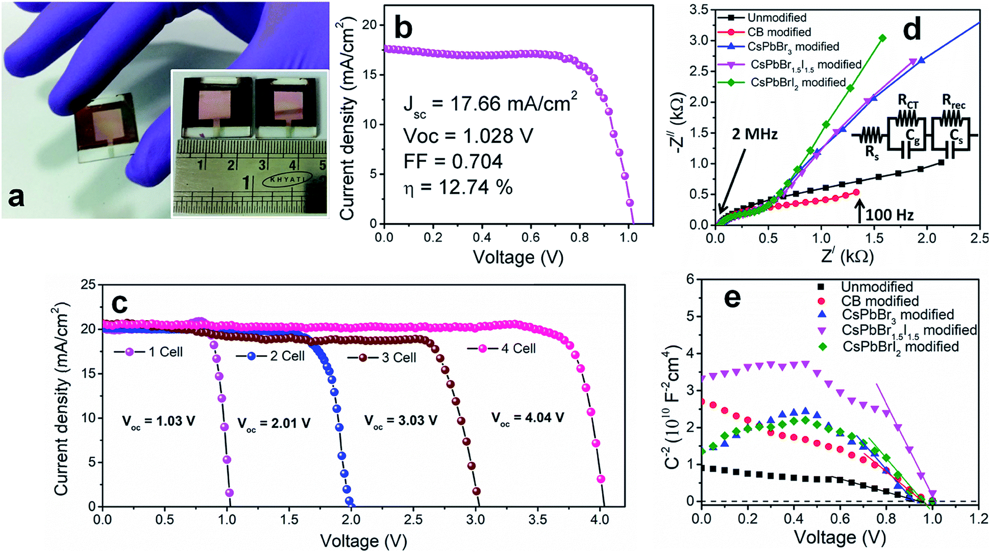 | ||
| Fig. 3 (a) Photograph and (b) J–V characteristics of the large area (1 cm2) CsPbBr1.5I1.5 QD modified devices. (c) J–V plots of 4 cells integrated in series. (d) Nyquist plots for the unmodified and CB, CsPbBr3, CsPbBr1.5I1.5 and CsPbBrI2 QD modified samples measured in the frequency range from 2 MHz to 100 Hz under simulated 100 mW cm−2 AM1.5 G illumination. The inset shows the equivalent circuit modeled to fit the Nyquist plots. (e) Mott–Schottky plots at 100 Hz for the unmodified and QD modified devices. | ||
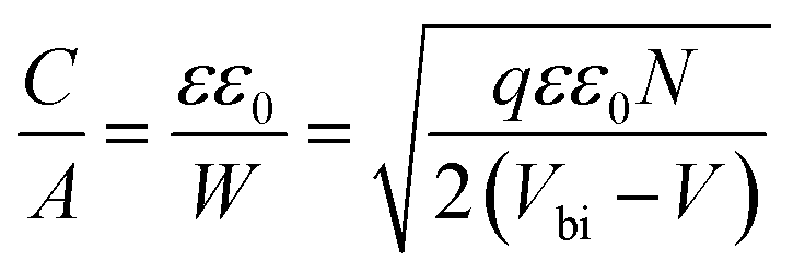
In order to further explore the interfacial characteristics of the devices, electrochemical impedance spectroscopy (EIS) was performed. The Nyquist plots measured at zero bias and 1 sun (100 mW cm−2) illumination consist of two diacritical characteristic arcs, one in the high frequency region due to the intrinsic dielectric properties of the perovskite and the other at low frequency arising from surface properties of the perovskite layer (Fig. 3d).31,32 The equivalent circuit shown in Fig. 3d (inset), used to fit the Nyquist plots, consists of an external series resistance (RS) accounting for the ohmic contribution of contacts and wires, geometrical capacitance (Cg) associated with the dielectric response of the perovskite in parallel with charge transfer resistance (RCT) associated with diffusion and transfer processes in the perovskite layer and accumulated capacitance (CS) associated with surface charge accumulation at the interfaces in parallel with recombination resistance (Rrec). The detailed fitting parameters for the representative Nyquist plots measured at 0 V are listed in Tables 1 and S3.† The fact that QD modification significantly eliminates the surface trap states is remarkably prominent from the increase of Rrec from 869 Ω for the unmodified device to 1662 Ω for the CB modified device and then again to 10102 Ω for the CsPbBr1.5I1.5 QD modified devices and a similar order of magnitude for the other two QD modified devices. Concurrently, the charge carrier lifetime (τe) determined by multiplying Rrec and CS (τe = Rrec × CS) shows an increase from 0.81 ms for the unmodified device to 4.5 ms for the CsPbBr1.5I1.5 QD modified devices (Table S3†). The Bode phase diagram (Fig. S15a†) shows two peaks, one in the high frequency region (104 to 106 Hz) attributed to charge transfer process and the other low frequency (102 to 103 Hz) peak arises due to charge recombination in the perovskite films.33 In the unmodified and CB modified devices, the charge recombination peak might appear at even lower frequencies, beyond the experimental range. We also varied the applied bias and the corresponding Nyquist plots are shown in Fig. S16.† The extracted Rrec values at different applied bias voltages of the QD modified devices are much higher than those of the unmodified device (Fig. S15b†). This reveals that the trap state removal via antisolvent-cum-QD treatment can effectively decrease the recombination of charge carriers at the interfaces. To gain more insight into the device, we performed Mott–Schottky analysis from the capacitance–voltage measurements at a low frequency of 100 Hz (Fig. 3e). According to the depletion approximation, junction capacitance (C) can be expressed as34
 | (1) |
 depicts a straight line where the intersection on the bias axis gives Vbi, the slope gives the impurity doping density N, and the depletion width corresponding to zero bias can be calculated by the relation31,34
 | (2) |
The voids and trap states associated with charge accumulation lower Vbi for the unmodified and CB modified devices compared to their respective VOC whereas trap state removal allows both Vbi and VOC to be proximal in the CsPbBr1.5I1.5 and CsPbBrI2 QD modified devices (Table 1). Moreover an increment in W to ∼156 nm with CsPbBr1.5I1.5 QD modification suggests the formation of a close to fully depleted junction with ∼250 nm TiO2 because of efficient charge separation and suppressed back reaction which consequently contribute to improved PCE.34
To evaluate the energy level alignment of the QDs, and unmodified and modified perovskite layers, UPS measurements were performed; the spectra are shown in Fig. S17† and the energy band diagram is shown in Fig. 4a, where Fermi level alignment is used instead of vacuum level alignment. The optical band gap of perovskite films is used to calculate the conduction band minimum (CBM) (Table S1†). A similar ligand removal approach was adapted for only QD deposited films and hence the UPS results could be meaningfully compared between the perovskite-QD and only QD films, without any interference from screening of the ligands. The work function decreases and the valence band maximum (VBM) shifts towards the Fermi level by QD modification of the perovskite film. The resulting energy band diagram suggests suitable alignment of the VBM and CBM for bulk perovskite with the QDs (except for CsPbBr3), ensuring smooth electron and hole transfer. The CBM of the perovskite layer increases upon CB and QD modifications, which significantly favours electron injection to TiO2.35 The superlative performance of the CsPbBr1.5I1.5 QD modified perovskite devices can be further unveiled from XPS analysis of the unmodified and CsPbBr1.5I1.5 QD modified perovskite films and CsPbBr1.5I1.5 QDs separately deposited on fluorine doped tin oxide glass. A survey scan of the CsPbBr1.5I1.5 modified perovskite films contains signatures of all the elements (Fig. S18a†). The binding energy difference between Pb 4f7/2 (138–139 eV) and Pb 4f5/2 (142–144 eV) is 4.85 eV and remains the same for all three samples (Fig. 4b). Low intensity peaks corresponding to Pb0 are only observed in unmodified films at lower binding energy (136.8 eV for 4f7/2 and 141.7 eV for 4f5/2) manifesting the removal of surface defects or impurity sites by QD modification.36 The CsPbBr1.5I1.5 QD modified film has a lower binding energy shift of 0.27 eV than the unmodified sample because of partial electron transfer from the grain boundary embedded QDs to the bulk perovskite through the interactions between the PbI6− framework in the bulk perovskite and Br− ions in CsPbBr1.5I1.5 QDs.37 Unlike a shift of 0.64 eV in the Pb 4f7/2 and 4f5/2 levels between bulk CH3NH3PbI3−xClx and CsPbBr1.5I1.5 QD modified films having different compositions, no significant shift is observed in the I 3d5/2 (618–619 eV) and I 3d3/2 (630–631 eV) levels (Fig. 4c). On the other hand, the Cs 3d spectrum is shifted by 0.43 eV towards higher binding energy from only CsPbBr1.5I1.5 QDs to the QD modified films as evident from the Cs 3d5/2 (724–725 eV) and Cs 3d3/2 (738–739 eV) levels (Fig. 4d). The C 1s core level of the unmodified and CsPbBr1.5I1.5 QD modified perovskite consists of two peaks, one at 286.5 eV representing the C–N bond in the methylammonium cation and the other at 284.9 eV from C–C and C–H bonds in adsorbed hydrocarbons during solution processed perovskite film preparation (Fig. 4e).38 The relative intensity of the C–N peak increases after QD modification, implying formation of larger perovskite grains and removal of surface defect states. The Cs+ bonding environment probed by XPS depth profiling of the CsPbBr1.5I1.5 QD modified film shows no change in the binding energy of the Cs 3d level or the valence band edge with etching time (Fig. S18b and c†). This further validates the absence of any mixed cation perovskite formation since Cs+ incorporation into CH3NH3PbI3−xClx would have slightly increased the band gap of the bulk perovskite.
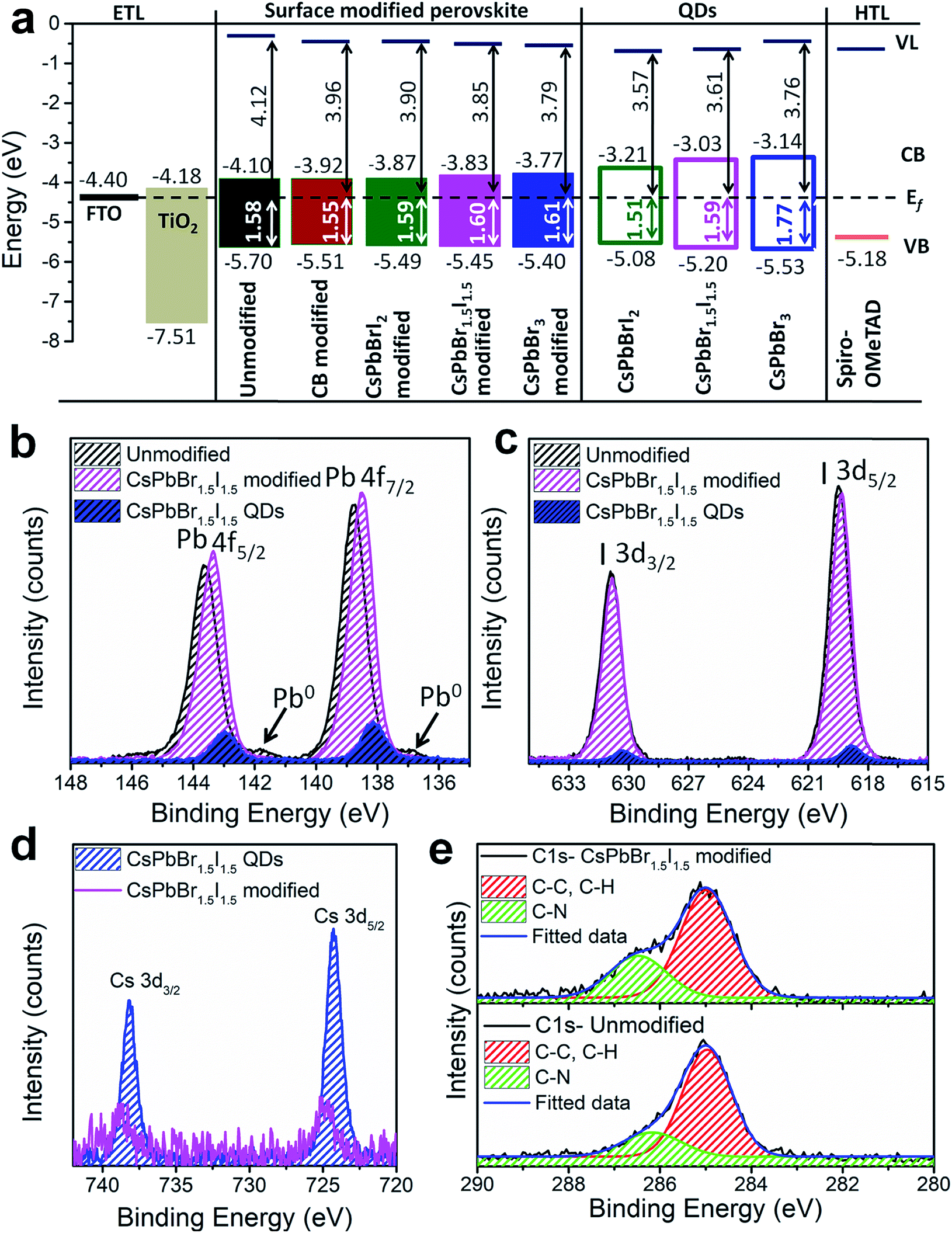 | ||
| Fig. 4 (a) Energy band diagram calculated from the UPS spectra. XPS spectra for (b) Pb 4f and (c) I 3d levels of the unmodified and CsPbBr1.5I1.5 QD modified perovskite films and CsPbBr1.5I1.5 QDs. (d) Cs 3d level spectra for the CsPbBr1.5I1.5 modified bulk perovskite and CsPbBr1.5I1.5 QDs. (e) C 1s spectra for the unmodified and CsPbBr1.5I1.5 QD modified bulk perovskite. | ||
The charge carrier transport dynamics has been investigated by optical pump white light super continuum probe fs-TAS, the experimental details of which are presented in Fig. S19.† The differential absorbance (ΔOD) spectra at several time delays between the pump and probe with a photo-excitation of 480 nm pump wavelength and a fluence of 7.5 μJ cm−2 are shown in Fig. 5a and b for the unmodified and CsPbBr1.5I1.5 QD modified perovskite films. The corresponding pseudo-color maps are shown in Fig. S20.† The transient absorption spectrum of the unmodified film shows a negative change in absorption at around 620–770 nm (Fig. 5a) with a prominent excitonic bleach signal at ∼730 nm (Fig. S20†) near the band gap (1.60 eV, Table S1†) of CH3NH3PbI3. TAS spectra also show the excited state absorption (ESA) in the range of 570–630 nm (Fig. 5a). The excitonic bleaching and ESA signals gradually decrease with the increase in delay time.39,40 The bleach position in the fs-TAS spectra, which corroborates the excitonic peak of the steady state absorption spectra (Fig. S7†), can be interpreted as the bleaching of excitonic absorption due to phase-space filling by free carriers or the presence of excitons. The ESA corresponds to the photo-induced absorption above the band gap due to the hot carriers.41,42 The transient bleach signal gets narrowed and experiences a blue shift to ∼715 nm due to CsPbBr1.5I1.5 QD modification (Fig. 5b) as the band gap of the unmodified perovskite increases by replacement of I− with Br− in the PbI6− framework.43 Therefore the position of the bleach signal of all the samples deposited on a quartz substrate, with or without an ETL/HTL, depends on the halide composition of the QDs (Table S4†).
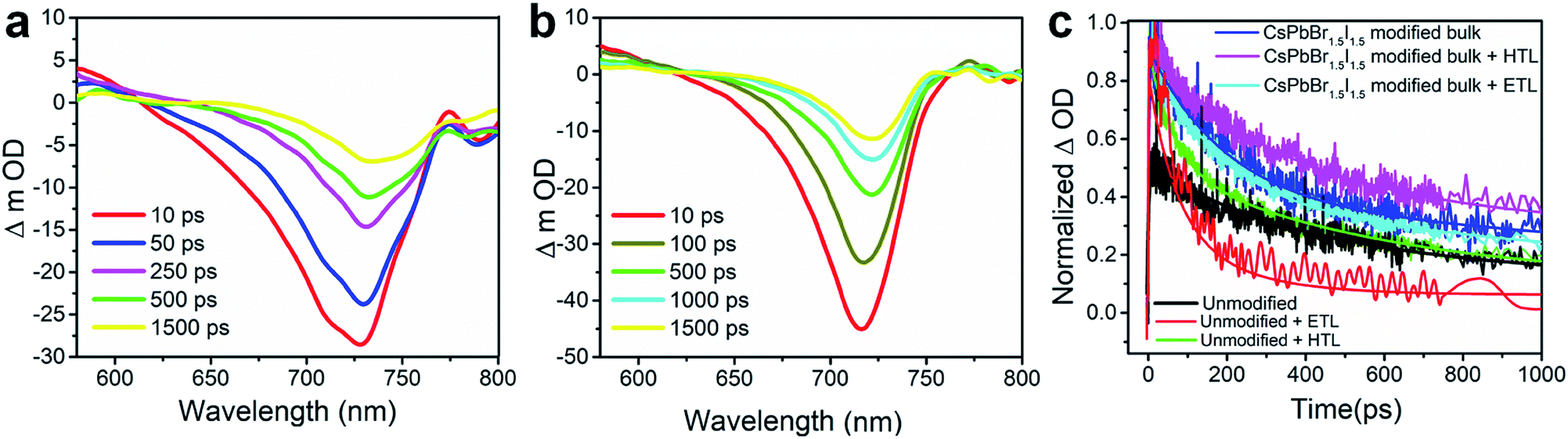 | ||
| Fig. 5 ΔOD versus wavelength variation from fs-TAS measurements for the (a) unmodified CH3NH3PbI3−xClx and (b) CsPbBr1.5I1.5 QD surface modified CH3NH3PbI3−xClx at different time delays after photo-excitation at 480 nm pump wavelength with a fluence of 7.5 μJ cm−2. (c) Transient bleach decay kinetics with their three corresponding exponential modified Gaussian fittings for the unmodified CH3NH3PbI3−xClx and CsPbBr1.5I1.5 QD modified films and with the ETL (TiO2) and HTL (spiro-OMeTAD). | ||
The relaxation dynamics of photo-excited bleaching of all the unmodified and modified films are studied separately with the ETL and HTL where the decay kinetics of the bleaching signals are measured and rigorously explored with decaying exponentials convoluted with an instrument response function (EMGD) to decipher the time components related with charge carrier transport between the perovskite film and ETL/HTL.39,40 The equation of the EMGD function employed is as follows:
 | (3) |
| Samples | τ 1 (ps) | τ 2 (ps) | τ 3 (ps) |
|---|---|---|---|
| Unmodified | 82 | 205 | 930 |
| Unmodified/ETL | 11 | 138 | 219 |
| Unmodified/HTL | 15 | 206 | 1994 |
| CsPbBr1.5I1.5 modified | 0.7 | 266 | 2864 |
| CsPbBr1.5I1.5 modified/ETL | 0.5 | 247 | 2878 |
| CsPbBr1.5I1.5 modified/HTL | 0.4 | 303 | 10838 |
Conclusions
It can be concluded in brief that interfacial modification of bulk perovskites by all-inorganic perovskite QDs is extremely rewarding both in terms of increasing the efficiency and improving the stability of the PV device. QD modification yields compact bulk perovskite grains that help in improving their crystallinity by reducing the amorphous intergranular interfaces. In our systematic investigation it is observed that the recombination centers and trap states are reduced by QD filling at the bulk grain boundaries, which also results in higher carrier lifetime. Through halide compositional variation in the QDs, the maximum sustainable PCE along with the best long term durability up to 720 h with <20% PCE degradation is observed with CsPbBr1.5I1.5 QDs. Not only does our approach improve both the PCE and stability of the devices, it also paves the way to achieve long term stability of perovskite solar cells in general without compromising their celebrated efficiency.Experimental section
Materials
Lead(II) bromide (PbBr2, 99.999% trace metal basis), lead(II) iodide (PbI2, 99.999% trace metal basis), cesium carbonate (Cs2CO3, reagent plus, 99%), octadecene (ODE, technical grade, 90%), oleylamine (OAm, 70%), and oleic acid (OAc, 90%) were purchased from Sigma-Aldrich. Hexane (fraction from petroleum) and methyl acetate (MeOAc, synthesis grade) were purchased from Merck. FTO (TCO 22-7, 2.2 mm thickness) and Ti-nanoxide (T/SP, particle size 20 nm) were purchased from Solaronix. Titanium isopropoxide (>97%), spiro-MeOTAD (>99%), bis(trifluoromethane)sulfonimide lithium salt (99.95%), 4-tert-butylpyridine (TBP, 96%), tris(2-(1H-pyrazol-1-yl)pyridine) cobalt(III) (>99%), and anhydrous chlorobenzene (99.8%) were purchased from Sigma-Aldrich.Synthesis of CsPbBrxI3−x (x = 1–2)
All inorganic CsPbBrxI3−x (x = 1–3) QDs were synthesized following previous reports with slight modifications.26,47Synthesis of CH3NH3X (X = I, Cl)
CH3NH3I was synthesized by reacting methylamine (CH3NH3) and hydroiodic acid (HI). 10 ml HI was added dropwise into 24 ml CH3NH3 at 0 °C in a round bottom flask under constant stirring for 2 h. CH3NH3Cl was synthesized by following the same procedure as above by replacing HI with HCl. The resulting solution was evaporated in a rotary evaporator at 55 °C whereby a light yellowish powder of CH3NH3I (MAI) was obtained. Snow white color crystals of MAI were collected after re-dissolving the obtained powder in absolute ethanol and re-precipitating it from diethyl ether. Thereafter, the as-obtained MAI powder was dried in a vacuum oven at 70 °C overnight.Preparation of bulk CH3NH3PbI3−xClx
A non-stoichiometric precursor solution of CH3NH3PbI3−xClx was obtained by dissolving 346 mg PbI2, 120 mg MAI and 51 mg MACl in 1 ml N,N-dimethylformamide (DMF). The solution was stirred overnight under N2 and filtered through a syringe filter of pore size 0.45 μm, before spin coating.Preparation of bulk Cs0.05(MA0.17FA0.83)0.95Pb(I0.83Br0.17)3
Bulk triple cation perovskite Cs0.05(MA0.17FA0.83)0.95Pb(I0.83Br0.17)3 was prepared by dissolving the corresponding precursor salts in DMF/DMSO (4:1) solvent. In a typical methodology, a solution of PbI2 (0.75 M), MAI (0.16 M), FAI (0.78 M), CsI (0.05 M) and PbBr2 (0.25 M) was dissolved in DMF/DMSO and stirred at 70 °C for 5–6 h. The solution was kept under stirring overnight in N2 and filtered through a syringe filter of pore size 0.45 μm, before spin coating.
Preparation of the compact TiO2 precursor
A dilute acidic solution was prepared by mixing diluted HCl (3:1) dropwise in 2.5 ml ethanol. This acidic solution was added dropwise to an ethanolic solution of titanium isopropoxide under constant stirring. The resulting solution was stirred for 30 min to yield a homogeneous, clear and transparent precursor solution.
Device fabrication
Perovskite solar cells were fabricated on fluorine doped tin oxide (FTO, Solaronix, TCO 22-7, 2.2 mm thickness) coated glass substrates of sheet resistivity 5–7 Ω □−1. The desired patterning of FTO coated glass substrates was carried out by wet chemical etching. Thereafter, the substrates were cleaned sequentially in soft soap solution, deionized water, acetone, and isopropyl alcohol for 10 min, and dried in a hot air oven overnight at 80 °C. The substrates were further placed inside an ultraviolet ozone cleaner for 5 min to remove organic residues. For depositing the compact TiO2 layer, the precursor solution was spin coated on the as-prepared and cleaned substrates at 2000 rpm for 30 s. These substrates were placed on a preheated hot plate at 100 °C for 10 min and sequentially annealed at 550 °C for 1 h in a box furnace. After annealing and cooling the substrates, a mesoporous TiO2 layer (dissolved in isopropanol at a concentration of 60 mg ml−1) was deposited at 2000 rpm for 30 s and the substrates were again annealed at 550 °C for 1 h. They were then transferred in a N2 filled glovebox for deposition of the perovskite layer and hole transport layer (HTL). 50 μl perovskite precursor solution was deposited onto the mesoporous TiO2 layer by spin coating at 4000 rpm for 30 s with an initial ramp of 1000 rpm for 5 s. For antisolvent chlorobenzene (CB)-modification, 50 μl anhydrous chlorobenzene was spooned onto the perovskite films 20 s after the spin started at 4000 rpm. QD modifications were performed in a similar fashion to the antisolvent CB treatment. At first the QDs were dispersed in different concentrations (2, 5, 10 and 15 mg ml−1) of anhydrous CB. 50 μl of these QD dispersions were spooned onto the perovskite films, exactly 20 s after the spinning started at 4000 rpm. After that, the films were dipped 2 times each in lead nitrate dissolved in methyl acetate for 2 s to remove the ligands present in the QD modified perovskite films. Thereafter, the perovskite films were annealed at 80 °C for 90 min. Then sequentially the spiro-MeOTAD HTL was deposited on top of the perovskite layer via spin coating a solution containing 72.3 mg ml−1 spiro-OMeTAD in CB, 28.8 μl 4-TBP, and 17.5 μl of LiTFSI (520 mg ml−1 in acetonitrile) at 2000 rpm for 30 s. The substrates were annealed at 80 °C on a preheated hot plate for 10 min and transferred to a thermal evaporator for the sequential deposition of the MoO3 and Au top electrode. Firstly, 9 nm MoO3 was deposited at a deposition rate of 0.1–0.3 Å s−1 and finally a 100 nm thick Au thin film was deposited using a shadow mask at a deposition rate of 0.3–1 Å s−1 and a base pressure of 5.5 × 10⁻⁶ Torr. The thicknesses of the deposited MoO3 and Ag films were estimated in situ using a quartz crystal thickness monitor.Characterization & measurements
FTIR spectra were recorded with a PerkinElmer Spectrum RX1. UV-vis absorbance spectra were recorded using a Jasco V-670 spectrophotometer. Room temperature PL spectra were recorded with a Horiba Jobin Yvon Fluorolog using a Xe lamp as the excitation source with an excitation wavelength of 480 nm. The XRD measurements were carried out with a Proto-AXRD powder X-ray diffractometer equipped with a Cu Kα (λ = 1.54059 Å) radiation source. Field emission scanning electron microscopy (FE-SEM) images were recorded using a Carl Zeiss SUPRA 55VP FE-SEM. Transmission electron microscopy (TEM) images were recorded at the DST-FIST facility, IISER Kolkata, on a JEOL JEM-2100F equipped with an energy dispersive X-ray analysis (EDAX) setup. To record the TEM images, STEM-HAADF images, selected area electron diffraction (SAED) patterns, EDAX spectra and elemental mapping images, the perovskite films were scooped from the substrate and dispersed in hexane followed by light sonication before drop casting on the Cu grids. Photovoltaic measurements were carried out using a Batsol Class AAA solar simulator (Model no. PEC-L01) under AM 1.5 G illumination conditions at an intensity of 100 mW cm−2 using a shadow mask. The XPS core-level spectra were recorded using a KRATOS-SUPRA spectrometer at UNISA (Florida Science Campus), South Africa with monochromatic Al Kα radiation having an excitation energy (hν) of 1486.6 eV and a base pressure of 1.2 × 10⁻⁸ Torr. The UPS spectra were recorded using the same spectrometer with He–I (hν = 21.22 eV) excitation and the base pressure was maintained at ∼1.2 × 10⁻⁹ Torr. The femtosecond transient absorption (fs-TA) spectra were recorded using Newport's transient absorption spectrometer with a regenerative amplified Ti:sapphire laser system from Coherent (808 nm, 80 fs, 3 mJ per pulse, and 1 kHz repetition rate). EQE spectra were measured using a 1/8 m monochromator (Oriel Cornerstone 130) and a Hewlett-Packard 34401A digital multimeter.Conflicts of interest
There are no conflicts to declare.Acknowledgements
The authors thank Dr Arghya Bandyopadhyay for the contact angle measurements and Dr Lokendra Kumar, Department of Physics, University of Allahabad for the XRD data of perovskite thin films. DG thanks the Science and Engineering Research Board (SERB), Department of Science and Technology (DST) for his fellowship under NPDF Project No. PDF/2016/000069. DKC thanks DST-SERB under sanction EMR/2016/001703 for his fellowship. The financial support under EMR/2016/001703 is duly acknowledged for successful execution of this work. The IIT Kharagpur team acknowledges the SGDRI (UPM) project for the femtosecond facility. BG acknowledges the financial support from the VR-CSET program of the University of South Africa.References
- M. Liu, M. B. Johnston and H. J. Snaith, Nature, 2013, 501, 395–398 CrossRef CAS PubMed.
- M. A. Green, A. Ho-Baillie and H. J. Snaith, Nat. Photonics, 2014, 8, 506–514 CrossRef CAS.
- S. D. Stranks, G. E. Eperon, G. Grancini, C. Menelaou, M. J. P. Alcocer, T. Leijtens, L. M. Herz, A. Petrozza and H. J. Snaith, Science, 2013, 342, 341–344 CrossRef CAS PubMed.
- NREL, Efficiency chart, https://www.nrel.gov/pv/assets/images/efficiencychart-20180716.jpg, 2018 Search PubMed.
- H. Zhou, Q. Chen, G. Li, S. Luo, T.-b. Song, H.-S. Duan, Z. Hong, J. You, Y. Liu and Y. Yang, Science, 2014, 345, 542–546 CrossRef CAS PubMed.
- J. H. Heo, H. J. Han, D. Kim, T. K. Ahn and S. H. Im, Energy Environ. Sci., 2015, 8, 1602–1608 RSC.
- J. You, L. Meng, T.-B. Song, T.-F. Guo, Y. Yang, W.-H. Chang, Z. Hong, H. Chen, H. Zhou, Q. Chen, Y. Liu, N. D. Marco and Y. Yang, Nat. Nanotechnol., 2016, 11, 75–81 CrossRef CAS PubMed.
- L. K. Ono and Y. Qi, J. Phys. Chem. Lett., 2016, 7, 4764–4794 CrossRef CAS PubMed.
- J.-W. Lee, H.-S. Kim and N.-G. Park, Acc. Chem. Res., 2016, 49, 311–319 CrossRef CAS PubMed.
- N. J. Jeon, J. H. Noh, Y. C. Kim, W. S. Yang, S. Ryu and S. I. Seok, Nat. Mater., 2014, 13, 897–903 CrossRef CAS PubMed.
- J. S. Manser, M. K. Saidaminov, J. A. Christians, O. M. Bakr and P. V. Kamat, Acc. Chem. Res., 2016, 49, 330–338 CrossRef CAS PubMed.
- J. C. Hamill Jr, J. Schwartz and Y.-L. Yueh-Lin Loo, ACS Energy Lett., 2018, 3, 92–97 CrossRef.
- C. Fei, B. Li, R. Zhang, H. Fu, J. Tian and G. Cao, Adv. Energy Mater., 2017, 7, 1602017 CrossRef.
- M. Xiao, F. Huang, W. Huang, Y. Dkhissi, Y. Zhu, J. Etheridge, A. Gray-Weale, U. Bach, Y.-B. Cheng and L. Spiccia, Angew. Chem., 2014, 126, 10056–10061 CrossRef.
- D.-Y. Son, J.-W. Lee, Y. J. Choi, I.-H. Jang, S. Lee, P. J. Yoo, H. Shin, N. Ahn, M. Choi, D. Kim and N.-G. Park, Nat. Energy, 2016, 1, 16081–16088 CrossRef CAS.
- J. Haruyama, K. Sodeyama, L. Han and Y. Tateyama, Acc. Chem. Res., 2016, 49, 554–561 CrossRef CAS PubMed.
- J.-W. Lee, S.-G. Kim, S.-H. Bae, D.-K. Lee, O. Lin, Y. Yang and N.-G. Park, Nano Lett., 2017, 17, 4270–4276 CrossRef CAS PubMed.
- N. Ahn, K. Kwak, M. S. Jang, H. Yoon, B. Y. Lee, J.-K. Lee, P. V. Pikhitsa, J. Byun and M. Choi, Nat. Commun., 2016, 7, 13422 CrossRef CAS PubMed.
- J. Lu, X. Lin, X. Jiao, T. Gengenbach, A. D. Scully, L. Jiang, B. Tan, J. Sun, B. Li, N. Pai, U. Bach, A. N. Simonov and Y.-B. Cheng, Energy Environ. Sci., 2018, 11, 1880–1889 RSC.
- Y. Lin, L. Shen, J. Dai, Y. Deng, Y. Wu, Y. Bai, X. Zheng, J. Wang, Y. Fang, H. Wei, W. Ma, X. C. Zeng, X. Zhan and J. Huang, Adv. Mater., 2017, 29, 1604545 CrossRef PubMed.
- J.-H. Lee, J. Kim, G. Kim, D. Shin, S. Y. Jeong, J. Lee, S. Hong, J. W. Choi, C.-L. Lee, H. Kim, Y. Yi and K. Lee, Energy Environ. Sci., 2018, 11, 1742–1751 RSC.
- A. Karani, L. Yang, S. Bai, M. H. Futscher, H. J. Snaith, B. Ehrler, N. C. Greenham and D. Di, ACS Energy Lett., 2018, 3, 869–874 CrossRef CAS.
- M. M. Tavakoli, S. M. Zakeeruddin, M. Grätzel and Z. Fan, Adv. Mater., 2018, 30, 1705998 CrossRef PubMed.
- R. N. Gayen, S. Hussain, D. Ghosh, R. Bhar and A. K. Pal, J. Alloys Compd., 2012, 531, 34–40 CrossRef CAS.
- S. D. Wolf, J. Holovsky, S.-J. Moon, P. Löper, B. Niesen, M. Ledinsky, F.-J. Haug, J.-H. Yum and C. Ballif, J. Phys. Chem. Lett., 2014, 5, 1035–1039 CrossRef PubMed.
- D. Ghosh, M. Y. Ali, D. K. Chaudhary and S. Bhattacharyya, Sol. Energy Mater. Sol. Cells, 2018, 185, 28–35 CrossRef CAS.
- P. Kumar, C. Bilen, B. Vaughan, X. Zhou, P. C. Dastoor and W. J. Belcher, Sol. Energy Mater. Sol. Cells, 2016, 149, 179–186 CrossRef CAS.
- Q. Wang, B. Chen, Y. Liu, Y. Deng, Y. Bai, Q. Dong and J. Huang, Energy Environ. Sci., 2017, 10, 516–522 RSC.
- W. Qiu, T. Merckx, M. Jaysankar, C. M. d. l. Huerta, L. Rakocevic, W. Zhang, U. W. Paetzold, R. Gehlhaar, L. Froyen, J. Poortmans, D. Cheyns, H. J. Snaith and P. Heremans, Energy Environ. Sci., 2016, 9, 484–489 RSC.
- L.-L. Gao, C.-X. Li, C.-J. Li and G.-J. Yang, J. Mater. Chem. A, 2017, 5, 1548–1557 RSC.
- S. Ye, H. Rao, Z. Zhao, L. Zhang, H. Bao, W. Sun, Y. Li, F. Gu, J. Wang, Z. Liu, Z. Bian and C. Huang, J. Am. Chem. Soc., 2017, 139, 7504–7512 CrossRef CAS PubMed.
- I. Zarazúa, S. Sidhik, T. Lopéz-Luke, D. Esparza, E. De la Rosa, J. Reyes-Gomez, I. Mora-Seró and G. Garcia-Belmonte, J. Phys. Chem. Lett., 2017, 8, 6073–6079 CrossRef PubMed.
- X. Xu, Z. Liu, Z. Zuo, M. Zhang, Z. Zhao, Y. Shen, H. Zhou, Q. Chen, Y. Yang and M. Wang, Nano Lett., 2015, 15, 2402–2408 CrossRef CAS PubMed.
- J. M. Luther, M. Law, M. C. Beard, Q. Song, M. O. Reese, R. J. Ellingson and A. J. Nozik, Nano Lett., 2008, 8, 3488–3492 CrossRef CAS PubMed.
- Y. Jiang, M. R. Leyden, L. Qiu, S. Wang, L. K. Ono, Z. Wu, E. J. Juarez-Perez and Y. Qi, Adv. Funct. Mater., 2018, 28, 1703835 CrossRef.
- B. Philippe, B.-W. Park, R. Lindblad, J. Oscarsson, S. Ahmadi, E. M. J. Johansson and H. Rensmo, Chem. Mater., 2015, 27, 1720–1731 CrossRef CAS.
- Y. Zhou, F. Wang, H.-H. Fang, M. A. Loi, F.-Y. Xie, N. Zhao and C.-P. Wong, J. Mater. Chem. A, 2016, 4, 16191–16197 RSC.
- B. Conings, J. Drijkoningen, N. Gauquelin, A. Babayigit, J. D'Haen, L. D'Olieslaeger, A. Ethirajan, J. Verbeeck, J. Manca, E. Mosconi, F. De Angelis and H.-G. Boyen, Adv. Energy Mater., 2015, 5, 1500477 CrossRef.
- L. Wang, C. McCleese, A. Kovalsky, Y. Zhao and C. Burda, J. Am. Chem. Soc., 2014, 136, 12205–12208 CrossRef CAS PubMed.
- K. Ishioka, B. G. Barker, M. Yanagida, Y. Shirai and K. Miyano, J. Phys. Chem. Lett., 2017, 8, 3902–3907 CrossRef CAS PubMed.
- Y. Yang, D. P. Ostrowski, R. M. France, K. Zhu, J. van de Lagemaat, J. M. Luther and M. C. Beard, Nat. Photonics, 2015, 10, 53–59 CrossRef.
- Y. Yang, Y. Yan, M. Yang, S. Choi, K. Zhu, J. M. Luther and M. C. Beard, Nat. Commun., 2015, 6, 7961 CrossRef CAS PubMed.
- E. M. Talbert, H. F. Zarick, A. Boulesbaa, N. Soetan, A. A. Puretzky, D. B. Geoheganb and R. Bardhan, Nanoscale, 2017, 9, 12005–12013 RSC.
- E. Serpetzoglou, I. Konidakis, G. Kakavelakis, T. Maksudov, E. Kymakis and E. Stratakis, ACS Appl. Mater. Interfaces, 2017, 9, 43910–43919 CrossRef CAS PubMed.
- S. Shao, M. Abdu-Aguye, T. S. Sherkar, H.-H. Fang, S. Adjokatse, G. t. Brink, B. J. Kooi, L. J. A. Koster and M. A. Loi, Adv. Funct. Mater., 2016, 26, 8094–8102 CrossRef CAS.
- C. Bi, Q. Wang, Y. Shao, Y. Yuan, Z. Xiao and J. Huang, Nat. Commun., 2015, 6, 7747 CrossRef CAS PubMed.
- A. Swarnkar, A. R. Marshall, E. M. Sanehira, B. D. Chernomordik, D. T. Moore, J. A. Christians, T. Chakrabarti and J. M. Luther, Science, 2016, 354, 92–95 CrossRef CAS PubMed.
Footnotes |
| † Electronic supplementary information (ESI) available: Experimental methods, supplemental discussion, UV-Vis and PL of QDs, FESEM, AFM, TEM and STEM-HAADF mapping, additional current density–voltage curves, stability plots, EIS analysis, UPS and XPS analysis, and fs-TAS setup and spectra. See DOI: 10.1039/c9sc01183h |
| ‡ Equal contribution. |
| This journal is © The Royal Society of Chemistry 2019 |