DOI:
10.1039/C9SC00889F
(Edge Article)
Chem. Sci., 2019,
10, 4141-4147
Spatiotemporal imaging of electrocatalytic activity on single 2D gold nanoplates via electrogenerated chemiluminescence microscopy†
Received
21st February 2019
, Accepted 6th March 2019
First published on 7th March 2019
Abstract
Uncovering the relationship between the structure, surface properties and electrochemical activity of nanoparticles is of great importance for constructing novel nanocatalysts and highly efficient electrocatalytic devices. Here we report a study of the heterogeneously distributed electrocatalytic activity on individual 2D gold nanoplates. On the basis of electrogenerated chemiluminescence (ECL) microscopy, the size, shape, and site-specific catalytic activity of 2D nanocrystals could be directly imaged at the single particle level with submicron resolution. Since the microelectrode effect with higher fluxes at the perimeter was offset by diffusion of excited species of Ru(bpy)32+, calculated by finite element simulation, the ECL distribution was supposed to be uniform on the micro-sized plates. Therefore, it is highly possible that the observed nonuniform ECL distribution at single nanoplates reflected distinct surface electrocatalytic activities at different sites. Furthermore, ECL microscopy allows continuous in situ imaging, which elucidates the time-varying changes in the spatial distribution of electrocatalytic activity on individual nanoplates, indicating that the corners and edges with more defect sites exhibit higher reactivity, but lower stability than the flat facet. We believe that real-time and high-throughput ECL microscopy may lead to more comprehensive understanding of reactivity patterns of single nanocatalysts.
Introduction
Nanomaterials, especially noble metal nanoparticles, have attracted intensive interest because of their unique electrocatalytic properties, giving them potential in numerous applied fields including energy conversion and storage.1,2 Understanding the relationship between the structure and the electrochemical reactivity of metal nanoparticles can provide useful instructions for the design of ideal catalyst materials.3 Owing to their structural dispersion, the active catalytic sites of nanoparticles are heterogeneously distributed, and may fluctuate dynamically.4 Therefore, it is highly desirable to develop techniques with high resolution both in time and space to measure the electrocatalytic activity on single nanocatalysts instead of an ensemble.
Electrochemical techniques including the use of nanoelectrodes and scanning electrochemical microscopy (SECM) allow for the electrocatalytic activity of individual nanoparticles to be probed.5,6 They are not restricted by diffraction limits and don't require any irradiation. On the other hand, these methods are limited by diffusion of species around the probe and a low throughput. Optical methods of surface plasmon resonance,7,8 surface-enhanced Raman scattering9 and super-resolution fluorescence microscopy10 are pioneering techniques for imaging the local electrocatalytic activities of single nanoparticles, which exhibit several advantages, including a high throughput and high spatial resolution. The limitation of optical techniques for electrochemical measurement is that the extrinsic illumination source may bias the electrochemical current.
Electrogenerated chemiluminescence (ECL) is the process of light emission by the excited state of a luminophore generated at the surface of electrodes.11 Although specific reactions and conditions are required for ECL imaging and the generation of radicals may influence the surface status of electrodes, as a non-invasive optical readout with high spatiotemporal resolution, ECL microscopy has been applied for the monitoring of electrochemical reactions on different electrode structures for decades. In 1987, Engstrom et al.12 reported direct observation of nonuniform current density resulting from the edge effects of the electrode. In 1999, Wightman's group explored ECL imaging of microelectrodes with different geometries under different potential pulse frequencies.13 Sojic's group14 reported mapping ECL reactivity in space, which provided insights into the ECL mechanistic route operating in bioassays. In recent years, ECL microscopy has been further applied to the direct imaging of individual nanomaterials.15–17 Our group reported the study of the catalytic activities of single Au–Pt Janus nanoparticles by ECL microscopy.18 Compared to monometal nanoparticles, the Janus structure exhibited enhanced ECL intensity and stability, which was ascribed to the different electron-transfer rates at the heterogeneous structure. Without extrinsic illumination and complicated set-ups, ECL microscopy provides a direct and high-throughput way to image the electrocatalytic activity of single nanoparticles in real time.
Herein, we explored the imaging of electrocatalytic activity on single 2D micro-sized gold nanocrystals with spatial and temporal resolution (Scheme 1). Stepping to the excitation potential, the luminophore Ru(bpy)32+ and co-reactant were both oxidized at the nanoplates and produced an excited-state product and emitted light, which was directly observed via an EMCCD. Despite the edge effect of the microelectrode, digital simulation considering both charge transfer reactions and homogeneous reactions involved in the ECL process indicated a uniform concentration profile of Ru(bpy)32+* on the micro-sized plates (1.0–4.0 μm) under a low potential pulse frequency (2.5 Hz). The heterogeneous ECL intensities observed at the flat facet, edge and corner were ascribed to the site-specific electrocatalytic activity at single gold nanoplates. The in situ dynamic fluctuations of the activities on single nanoplates were also monitored with spatiotemporal resolution. Although as a mass transfer-controlled light emitting process, the diffusion of reactants resulted in broadening seen outside the 2D structures, real-time ECL microscopy using Ru(bpy)32+ as the luminophore realized relatively accurate imaging with submicron spatial resolution on the millisecond scale. Therefore, the presented ECL microscopy should find promising applications in the assessment of nanomaterials.
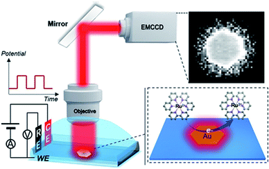 |
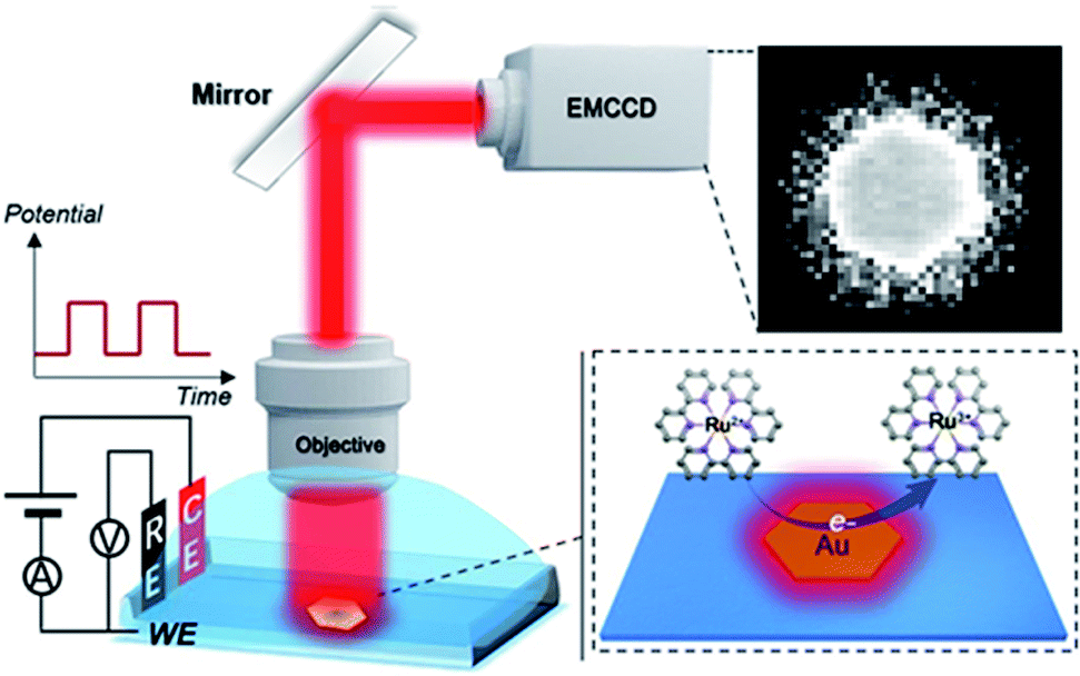
| | Scheme 1 Schematic illustration of ECL imaging of electrocatalytic activity on single 2D nanocatalysts. ITO as the working electrode (WE), Ag/AgCl as the reference electrode (RE) and Pt wire as the counter electrode (CE) were used. | |
Results and discussion
Characterization of 2D gold nanoplates
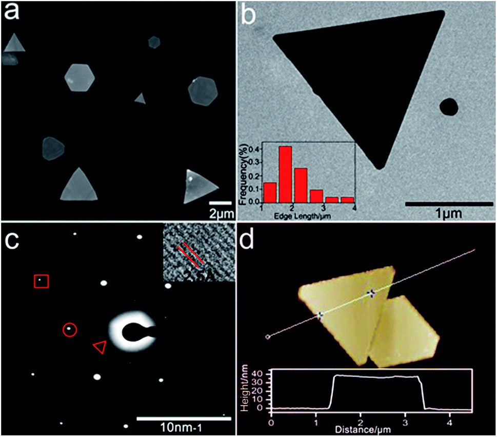
Noble metal nanoparticles (Au, Pt, and Ag) are well known for their electrocatalytic activities.19–21 2D gold nanoplates were synthesized according to the literature with slight modification of reaction conditions.22Fig. 1 shows the characterization of the gold nanoplates, which are mostly triangular and hexagonal with the edge length in the range of 1–4 μm (Fig. 1a and b) and a thickness of 40 nm ± 2 nm (Fig. 1d). The lattice spacing (2.5 Å) agrees well with the (111) lattice spacing of the gold single-crystal structure (Fig. 1c, inset), which is consistent with SAED analysis (Fig. 1c), as reported previously.23 The UV-vis absorption and plasmon scattering were also characterized and the results are displayed in Fig. S1.† Furthermore, the CTAB surfactant, which greatly hinders the electrochemical activity of the nanoplates, has to be removed before ECL imaging. Here we treated the surface of the nanoplates with UV/ozone for 30 min, which could efficiently remove the organic components without influencing the morphology of the nanocrystals24 (Fig. S2†). It has been reported that UV/ozone treatment for over 1 h could cause the oxidation of gold.25 And the gold oxide greatly reduced the generation of ECL.18 Here as shown in Fig. S3,† after removing CTAB, the ECL image of single nanoplates at 1.2 V vs. Ag/AgCl displayed good resolution, indicating that the structure of the gold nanoplates was barely influenced under current pretreatment conditions.
 |
| | Fig. 1 Characterization of 2D gold nanoplates. (a) Typical SEM images of the nanoplates. (b) TEM images of single triangular gold nanoplates. Inset: corresponding nanoplate edge length distribution diagram obtained with 77 nanoplates. (c) Selected area (electron) diffraction (SAED) from one nanoplate. The spots are marked by a triangle, circle, and box corresponding to 1/3(422), (220), and (422) diffractions, respectively. Inset: HRTEM image of part of the nanoplate. (d) Typical AFM image of the gold nanoplate and its height profile. | |
Spatial distribution of ECL intensity on single gold nanoplates
For the ECL imaging, gold nanoplates were immobilized on an ITO substrate based on electrostatic adsorption. The electrolyte was 10 mM phosphate buffer containing 1 mM Ru(bpy)32+ and 20 mM TPrA. As ECL is a mass transfer controlled light emitting process,26 under long-time excitation by applying cyclic voltammetry, the light emitting species spread around the visual field and created a blurred-looking image. Therefore, we adopted double potential step chronoamperometry from 0 V to 1.2 V vs. Ag/AgCl with a short excitation time period of 400 ms (2.5 Hz).
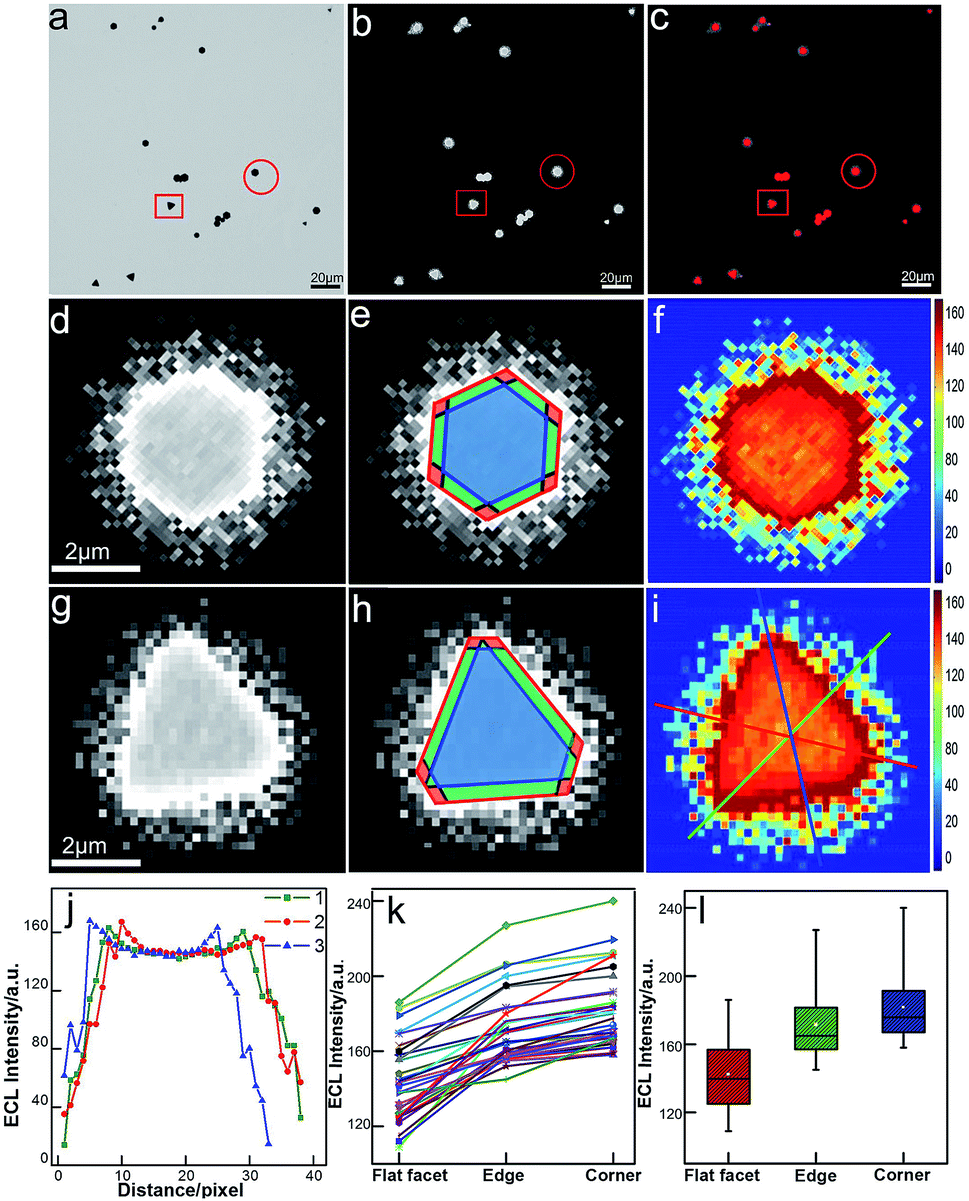
Unlike conventional electrochemical methods that measure current associated with electrochemical reactions taking place on the surface of electrodes,27 ECL microscopy measures the local generation of luminescence caused by the reactions near the electrode. Therefore, it allows for high-throughput and spatiotemporal resolved imaging. The bright-field, ECL (taken in the first potential step) and false-color overlaid images are shown in Fig. 2. Compared with our previous study with a smaller sized Janus particle (60 nm),18 the micro-sized gold nanoplates with a larger surface area exhibited higher ECL imaging resolution on supporting ITO. Two typical gold nanoplates (marked with a red circle and square) were chosen for the measurement of surface ECL distribution. As shown in Fig. 2d and g, the shapes (triangle and hexagon) of the nanoplates are clear. Each nanoplate could be divided into three regions: corner (red), edge (green), and flat facet (blue) according to the contour of the plates obtained from the bright-field image and the transient ECL profiles (Fig. 2e and h). The ECL intensities were further programmed using Matlab to obtain more intrinsic images with high color contrast. As shown in Fig. 2f and i, it is obvious that the distribution of ECL responses is nonuniform. We used three measuring lines that passed through the corners, edges and facets to determine the ECL distribution. The results show a similar ECL gradient (corners > edges > flat facets) (Fig. 2j). We did statistical analysis based on 35 nanoplates with different sizes and shapes. The ECL distributions on these plates generally follow the same trend (Fig. 2k). With further statistical analysis (Fig. 2l) of ECL intensities in different regions, it was found that corners have ∼6% higher ECL intensity than edges, and ∼30% higher intensity than flat facets.
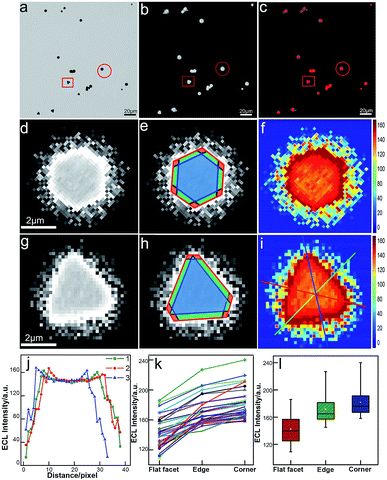 |
| | Fig. 2 Spatial distribution of ECL intensity on single gold nanoplates. (a) Bright-field image, (b) ECL image (exposure time: 200 ms) and (c) false-color overlay of the bright-field and ECL images. (d and g) Magnified areas of the ECL image (b) marked by a red circle and square. (e and h) Divided regions of corners (red), edges (green), and the flat surface facet (blue) in the ECL images of (e and h). (f and i) 2D spatial distribution ECL intensity obtained by using Matlab. (j) ECL intensity gradients at three measuring lines marked in (i). (k) Statistical site-specific ECL intensity of 35 nanoplates. (l) Box charts of the ECL intensities from corner, edge and flat facet regions. | |
Explanation of the spatial resolved ECL intensity on gold nanoplates
There are two possible reasons which could explain such a phenomenon. First, the nonuniform current density over the electrode surface due to an edge-dominated flux. In 1999, Wightman's group reported the spatial nonuniformity of ECL response at microelectrodes.13 They ascribed the spatial heterogeneity of ECL to nonuniform potential across the electrode with very short pulses (50 kHz frequency). On the other hand, under low frequencies (<500 Hz), the ECL appeared to be uniform across the surface. Second, the growth dependent surface defect results in the site-specific activity of the gold nanoplates.22 To find the predominant reason, COMSOL simulation was performed using finite difference methods in order to predict the generation rate of Ru(bpy)33+ and the ECL spatial profiles at triangular and hexagonal micro-structures. Unlike a potential pulse with a very high frequency, at a potential of 1.2 V vs. Ag/AgCl with a period of 400 ms, the interfacial potential reaches the desired value and 12 reactions could be involved in the ECL response (Table S1†).28 For digital simulation, two charge transfer reactions and four homogeneous reactions including radiative decay were considered (Table 1). The detailed process of modeling is described in the ESI.†
Table 1 Reactions and parameters applied for digital simulation of the ECL processa
| Charge transfer reactions |
E
0 (V) vs. Ag/AgCl |
k
0 (cm s−1) |
|
P stands for TPrA after losing two electrons.
|
| (1) Ru(bpy)33+ + e− → Ru(bpy)32+ |
1.06 |
0.02 |
| (2) TPrA˙+ + e− → TPrA |
0.90 |
0.6 |
| Homogeneous reactions |
k
f
|
| (3) TPrA˙+→ TPrA˙ + H+ |
537 (s−1) |
| (4) Ru(bpy)32++ TPrA˙ → Ru(bpy)3+ + P |
1010 (M−1 s−1) |
| (5) Ru(bpy)3+ + Ru(bpy)33+ → Ru(bpy)32+* + Ru(bpy)32+ |
1010 (M−1 s−1) |
| (6) Ru(bpy)32+* → Ru(bpy)32+ + hv |
107.2 (s−1) |
To determine the heterogeneous electron transfer rate constant of the Ru(bpy)32+/3+ redox pair, we did the calibration between the ECL intensity and current density using microelectrodes with a diameter from 12.5 μm to 100.0 μm (Fig. S4†). As displayed in Fig. S4f,† the ECL emission intensity is linear to the current density at the microelectrode resulting from the Ru(bpy)32+/Ru(bpy)33+ redox reaction. Based on the fitted linear equation, the heterogeneous reaction rate constant k0 could be calculated according to eqn (1) deduced from the Butler–Volmer (B–V) formalism at the initial time (t = 0).
| | iox = FAk0CR![[thin space (1/6-em)]](https://www.rsc.org/images/entities/char_2009.gif) e(1−α)f(E−E0′) e(1−α)f(E−E0′) | (1) |
where
F is Faraday's constant (96
485 C mol
−1),
α is the transfer coefficient taken as 0.5,
CR is the initial concentration of Ru(bpy)
32+ and
f =
F/
RT (38.92 V
−1). The potential difference of (
E −
E0′) = 140 mV. The average
k0 on a single gold nanoplate was determined to be 0.02 cm s
−1. As displayed in
Fig. 3a and d, the generation rate of Ru(bpy)
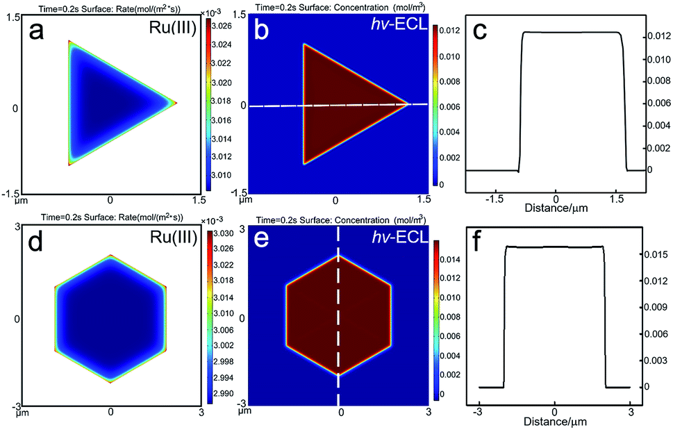
33+ on the electrode follows the trend of corners > edges > flat facets, which should be attributed to the higher diffusional fluxes at the perimeter of the micro-sized plates. However, in the surface concentration profiles of Ru(bpy)
32+* (
Fig. 3b and e), quite uniform ECL distributions were obtained. The ECL intensities at measuring lines that passed through the corners, edges and facets rarely varied (
Fig. 3c and f). It was found that the lifetime of the excited Ru(bpy)
32+* had a great impact on its concentration profile. We varied the decay rate of Ru(bpy)
32+* to 10
4 s
−1 in 3D COMSOL simulation. The simulated ECL profile shows a gradient with flat facets > perimeter (Fig. S7
†). On the other hand, with a 10
10 s
−1 decay rate, the ECL distribution is the opposite (Fig. S8
†). With a longer lifetime, the distribution of Ru(bpy)
32+* is greatly influenced by the edge dominated flux. Therefore, although more excited species are generated at the edges, the higher flux could result in a lower concentration. Here, the digital simulation shows that with the measured decay rate of Ru(bpy)
32+* as 10
7.2 s
−1,
29 the microelectrode effect with higher fluxes at the perimeter is offset and the ECL distribution at micro-sized gold plates is supposed to be uniform. Hence, with the Ru(bpy)
32+/TPrA pair, the influence from the microelectrode effect on the ECL spatial distribution is limited. Therefore, it is highly possible that the predominant reason for the nonuniform ECL distribution on 2D gold nanoplates observed under microscopy is their site-specific activity. The growth-dependent surface defects that come from the decaying 2D growth rate when the nanoplate grows from a seed by the thermal aqueous solution method could result in heterogeneous electrocatalytic activities on individual nanoplates.
22,30
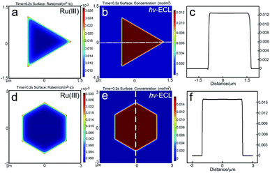 |
| | Fig. 3 Results of the simulated reaction rate and concentration profiles. The generation rate of Ru(III) on the gold (a) triangular and (d) hexagonal nanoplates. The ECL spatial intensity distribution on the gold (b) triangular and (e) hexagonal nanoplates. (c and f) The distribution of ECL intensity at the measuring line marked in (b and e). | |
Spatiotemporal resolved electrocatalytic activity on single gold nanoplates
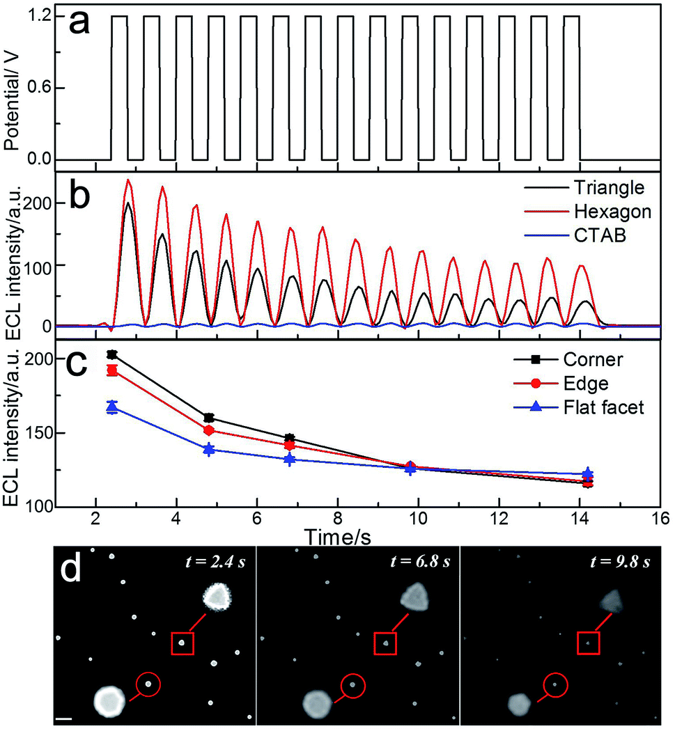
The intrinsic heterogeneity can also cause the temporally varying electrochemical catalytic activity of nanomaterials.31 It is desirable to understand the spatial changes in catalytic activity with time lapsed at the single nanoparticle level. Fig. 4 shows the applied potential waveform (Fig. 4a) and the ECL intensity trajectories (Fig. 4b) in 10 mM phosphate buffer containing 1 mM Ru(bpy)32+ and 20 mM TPrA at single triangular and hexagonal nanoplates with 15 potential cycles. As previously stated, after treatment with UV/ozone, strong ECL intensity could be observed at the gold nanoplates. The images taken by ECL microscopy are shown in Fig. 4d. At the initial time (2.4 s), the gold nanoplates were bright with high resolution. The ECL intensity of the gold nanoplates decreased along with the increasing number of potential cycles. Since the morphologies of the nanoplates were barely changed after several potential steps (Fig. S5†), the decrease of ECL was mainly ascribed to the surface oxidation. In the magnified areas of ECL images (inset of Fig. 4d), the shapes of the gold nanoplates could be observed directly. However, the distributions of the ECL intensities in different regions are time-dependent. Along with increasing time, the surface was gradually oxidized, causing both the decrease of ECL intensity and a blurred outline. Fig. 4c shows the ECL intensities in different regions of the gold nanoplates vs. time trajectory. During the observation time period, the difference of intensities between corner, edge and center areas dropped. Over 10 s observation, more ECL emitters formed on the flat facet instead of the corner and edge, suggesting that the sites with higher electrocatalytic activities showed lower stability during the redox reactions. The spatiotemporal fluctuation of the catalytic activity of single gold nanoplates is consistent with the report using super-resolution fluorescence microscopy,32 but the real-time ECL imaging achieved much higher temporal resolution (millisecond).
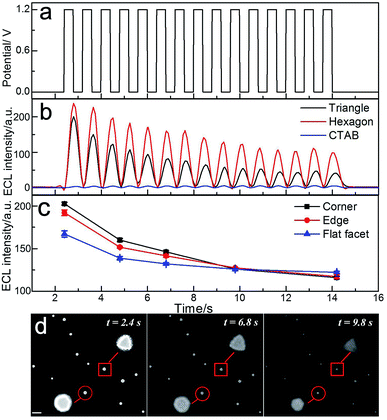 |
| | Fig. 4 Spatiotemporal ECL imaging of electrocatalytic activity on single gold nanoplates. (a) Applied potential-time traces and (b) integrated ECL intensities of single triangular (black) and hexagonal nanoplates (red), and CTAB coated nanoplates (blue) from control measurement. (c) Time-lapsed ECL intensities from the corner, edge and flat facet regions of the triangular nanoplate and (d) corresponding ECL images taken at 2.4 s, 6.8 s and 9.8 s. | |
Conclusions
In summary, we have demonstrated the potential of ECL microscopy to image the electrocatalytic activity of 2D micro-sized gold nanoplates at the individual particle level with spatiotemporal resolution. With the Ru(bpy)32+/TPrA pair, the influence from the microelectrode effect to the ECL spatial distribution is limited, and the in situ ECL imaging closely reflects the real electrocatalytic activity of the 2D plates with submicron resolution. This technique is direct, fast, and quantitative with a low requirement for equipment, which makes it suitable for direct imaging and rapid screening of the electrocatalytic activities of nanomaterials. Despite the success of ECL imaging in electrochemical study, some aspects are still challenging. First, as ECL is a mass transfer controlled light emitting process, the diffusion of emitters influenced the accuracy of imaging. In addition, restricted by its diffraction limits, ECL microscopy cannot reach ultra-high resolution now. However, the unique specialties of ECL microscopy for electrochemical process study attract us to devote efforts to the development of this technique. We believe that ECL microscopy has great potential for the study of the properties of nanomaterials.
Experimental
Chemicals and materials
Tripropylamine (TPrA), HAuCl4·3H2O and Ru(bpy)3Cl2 were purchased from Sigma-Aldrich (USA). Sodium citrate dehydrate and hexadecyltrimethylammonium bromide (CTAB) were purchased from Aladdin (Shanghai, China). 10 mM sterile phosphate buffered saline (PBS, PH 7.4) was purchased from KeyGEN Biotech (Nanjing, China). Indium tin oxide (ITO)-coated glass slides (coating thickness, ∼10 nm; resistance, 8–12 Ω m−2) were purchased from SPI Supplies. Sylgard 184 (including the PDMS monomer and curing agent) and plastic culture dishes were purchased from Dow Corning (Midland, MI, USA). All solutions were prepared with Millipore water (Millipore, Inc., Bedford, MA) treated with a 0.22 μm filter (PES membrane, Merck Millipore Ltd), and stored at 4 °C in a refrigerator.
Apparatus
The morphologies of the gold nanoplates were characterized using a JEOL200CX transmission electron microscope (TEM) operated at 200 kV. Selected area (electron) diffraction (SAED) and HRTEM images were obtained on a JEM-2100F (JEOL Ltd., Japan). Scanning electron microscopy (SEM) images were obtained from an S-3000 N scanning electron microscope (Tokyo, Japan). Atomic force microscopy (AFM) images were recorded on a 5500 Atomic Force Microscope (Agilent Technologies, USA). UV-vis absorption spectra were recorded on a SHIMADZU UV-3600 spectrophotometer (Japan). The scattering spectrum was obtained with a monochromator (Acton SP2358, PI, USA) (grating density: 300 lines per mm; blazed wavelength: 500 nm) combined with liquid nitrogen cooled PyLoN ccd cameras (Princeton Instruments, USA). Traditional electrochemical measurements were performed using a CHI-630A (CH Instruments Co.) with a three-electrode system at room temperature.
Synthesis of gold nanoplates
First, 14.5 mL deionized water was heated in a three-neck flask to 80 °C with stirring. Then 0.5 mL 25 mM trisodium citrate solution was added. After 1 min, 10 mL solution containing 1.25 mM HAuCl4 and 7.5 mM CTAB which was preheated to 50 °C was added to the trisodium citrate solution. The solution was refluxed by connecting one neck of the flask to a condenser. The resulting solution turned from orange to light yellow and then to colorless in 3 min indicating the gradual formation of large gold structures. The reaction was continued for 45 min before removing the heating mantle from the flask. To collect the nanoplates, the mixture was centrifuged at 3000 rpm for 10 min and then the supernatant was removed. After washing and precipitation, the obtained gold nanoplates were dispersed in 5 mL water. The gold nanoplates were easily separated from the mixture containing gold spherical nanoparticles and nanorods by several rounds of gravity sedimentation.
Sample immobilization on ITO
The indium tin oxide (ITO) glass slides (3.5 × 2 cm) were cleaned by sonication in 2-propanol, alcohol and 18.2 MΩ cm water for 15 min each. Then, the slides were dried in a N2 atmosphere and transferred to a clean Corning plastic dish for treatment in a PSD-UV4 ozone system (Novascan Technologies) for 30 min to remove the organic residues. Next, a 200 μL diluted gold nanoplate suspension was drop-cast onto a cleaned ITO slide and electrostatically adsorbed for 4 h. Then, the slide was washed with distilled water 3 times to remove the gold nanoplates that were not adsorbed. Finally, the glass side was placed in the PSD-UV4 ozone system (Novascan Technologies) for 30 min to remove ligands on the surface of the gold plates.
ECL microscopy setup
The ECL microscopy setup was on based on an Olympus IX53 upright microscope with a water immersion objective (60× , NA 1.0, Olympus, Japan). A CHI660E electrochemical workstation (CH Instruments Co., China) was applied to control the ECL reactions. An electron multiplying CCD (EMCCD) (Andor iXon Ultra 888) was applied to obtain images. The time resolution of image acquisition was 200 ms. The ECL imaging was performed in a shielding room. Ag/AgCl and Pt wire (0.5 mm diameter) were used as the reference and counter electrodes. ITO with gold nanoplates immobilized on its surface was used as the working electrode. The electrolyte was 300 μL 10 mM phosphate buffer containing 1 mM Ru(bpy)32+ and 20 mM TPrA. We adopted double potential step chronoamperometry from 0 V to 1.2 V vs. Ag/AgCl with a short time interval of 400 ms.
For the ECL imaging of commercial gold microelectrodes (12.5, 25, 50 or 100 μm in diameter), the Olympus IX73 inverted microscope and the same EMCCD (Andor iXon Ultra 888) were applied. The microelectrodes were placed above a 0.17 mm coverslip controlled by using an Eppendorf TransferMan-4r motorized micromanipulator (Eppendorf Instrument Co.). All other setups and reactants are exactly the same as ECL imaging of single nanoplates.
Synchronous triggering of the EMCCD and electrochemical workstation
The EMCCD and electrochemical workstation were synchronized by using a Digital delay/pulse generator DG535(Stanford Research Systems, Inc.) Two TTL signals were sent to the electrochemical workstation and EMCCD simultaneously to trigger the reaction and recording. The rise time of the TTL signal was less than 3 ns and the time delay of the two TTL signals is ca. 5 ps.
COMSOL simulation
The finite element simulation of ECL distribution on triangular and hexagonal gold nanoplates was carried out with COMSOL Multiphysics software v5.3a with three-dimensional finite element modeling. The details of the simulation are shown in ESI† part 6.
Conflicts of interest
The authors declare no competing financial interest.
Acknowledgements
This work was supported by the National Natural Science Foundation (Grants 21327902, 21535003, and 21605079) of China, and Fundamental Research Funds for the Central Universities.
References
- S. Park, Y. Shao, J. Liu and Y. Wang, Energy Environ. Sci., 2012, 5, 9331–9344 RSC.
- K. Tedsree, T. Li, S. Jones, C. W. A. Chan, K. M. K. Yu, P. A. J. Bagot, E. A. Marquis, G. D. W. Smith and S. C. E. Tsang, Nat. Nanotechnol., 2011, 6, 302–307 CrossRef CAS PubMed.
- J. W. Hong, S. W. Kang, B.-S. Choi, D. Kim, S. B. Lee and S. W. Han, ACS Nano, 2012, 6, 2410–2419 CrossRef CAS PubMed.
- I. L. C. Buurmans and B. M. Weckhuysen, Nat. Chem., 2012, 4, 873–886 CrossRef CAS PubMed.
- T. Sun, Y. Yu, B. J. Zacher and M. V. Mirkin, Angew. Chem., Int. Ed., 2014, 53, 14120–14123 CrossRef CAS PubMed.
- J. Kim, C. Renault, N. Nioradze, N. Arroyo-Currás, K. C. Leonard and A. J. Bard, J. Am. Chem. Soc., 2016, 138, 8560–8568 CrossRef CAS PubMed.
- X. Shan, U. Patel, S. Wang, R. Iglesias and N. Tao, Science, 2010, 327, 1363–1366 CrossRef CAS PubMed.
- X. Shan, I. Diez-Perez, L. Wang, P. Wiktor, Y. Gu, L. Zhang, W. Wang, J. Lu, S. Wang, Q. Gong, J. Li and N. Tao, Nat. Nanotechnol., 2012, 7, 668–672 CrossRef CAS PubMed.
- A. J. Wilson and K. A. Willets, Nano Lett., 2014, 14, 939–945 CrossRef CAS PubMed.
- T. Chen, Y. Zhang and W. Xu, ACS Nano, 2016, 10, 8434–8442 CrossRef CAS PubMed.
- M. M. Richter, Chem. Rev., 2004, 104, 3003–3036 CrossRef CAS PubMed.
- R. C. Engstrom, C. M. Pharr and M. D. Koppang, J. Electroanal. Chem. Interfacial Electrochem., 1987, 221, 251–255 CrossRef CAS.
- R. G. Maus, E. M. McDonald and R. M. Wightman, Anal. Chem., 1999, 71, 4944–4950 CrossRef CAS PubMed.
- M. Sentic, M. Milutinovic, F. Kanoufi, D. Manojlovic, S. Arbault and N. Sojic, Chem. Sci., 2014, 5, 2568–2572 RSC.
- S. Pan, J. Liu and C. M. Hill, J. Phys. Chem. C, 2015, 119, 27095–27103 CrossRef CAS.
- A. J. Wilson, K. Marchuk and K. A. Willets, Nano Lett., 2015, 15, 6110–6115 CrossRef CAS PubMed.
- C. Ma, W. Wu, L. Li, S. Wu, J. Zhang, Z. Chen and J.-J. Zhu, Chem. Sci., 2018, 9, 6167–6175 RSC.
- M.-J. Zhu, J.-B. Pan, Z.-Q. Wu, X.-Y. Gao, W. Zhao, X.-H. Xia, J.-J. Xu and H.-Y. Chen, Angew. Chem., Int. Ed., 2018, 130, 4074–4078 CrossRef.
- J. Chen, B. Lim, E. P. Lee and Y. Xia, Nano Today, 2009, 4, 81–95 CrossRef CAS.
- G. G. Li, Y. Lin and H. Wang, Nano Lett., 2016, 16, 7248–7253 CrossRef CAS PubMed.
- M. Arenz, K. J. J. Mayrhofer, V. Stamenkovic, B. B. Blizanac, T. Tomoyuki, P. N. Ross and N. M. Markovic, J. Am. Chem. Soc., 2005, 127, 6819–6829 CrossRef CAS PubMed.
- W.-L. Huang, C.-H. Chen and M. H. Huang, J. Phys. Chem. C, 2007, 111, 2533–2538 CrossRef CAS.
- J. E. Millstone, S. Park, K. L. Shuford, L. Qin, G. C. Schatz and C. A. Mirkin, J. Am. Chem. Soc., 2005, 127, 5312–5313 CrossRef CAS PubMed.
- C. Aliaga, J. Y. Park, Y. Yamada, H. S. Lee, C.-K. Tsung, P. Yang and G. A. Somorjai, J. Phys. Chem. C, 2009, 113, 6150–6155 CrossRef CAS.
- D. E. King, J. Vac. Sci. Technol., A, 1995, 13, 1247–1253 CrossRef CAS.
- W. Miao, J.-P. Choi and A. J. Bard, J. Am. Chem. Soc., 2002, 124, 14478–14485 CrossRef CAS PubMed.
- B. M. Quinn, P. G. van't Hof and S. G. Lemay, J. Am. Chem. Soc., 2004, 126, 8360–8361 CrossRef CAS PubMed.
- R. M. Wightman, S. P. Forry, R. Maus, D. Badocco and P. Pastore, J. Phys. Chem. B, 2004, 108, 19119–19125 CrossRef CAS.
- C. T. Lin, W. Boettcher, M. Chou, C. Creutz and N. Sutin, J. Am. Chem. Soc., 1976, 98, 6536–6544 CrossRef CAS.
- X. Sun, S. Dong and E. Wang, Angew. Chem., Int. Ed., 2004, 116, 6520–6523 CrossRef.
- W. Xu, J. S. Kong, Y.-T. E. Yeh and P. Chen, Nat. Mater., 2008, 7, 992–996 CrossRef CAS PubMed.
- Y. Zhang, J. M. Lucas, P. Song, B. Beberwyck, Q. Fu, W. Xu and A. P. Alivisatos, Proc. Natl. Acad. Sci. U. S. A., 2015, 112, 8959–8964 CrossRef CAS PubMed.
Footnotes |
| † Electronic supplementary information (ESI) available: Additional figures, additional results and discussion and details for digital simulation. See DOI: 10.1039/c9sc00889f |
| ‡ These authors contributed equally. |
|
| This journal is © The Royal Society of Chemistry 2019 |
Click here to see how this site uses Cookies. View our privacy policy here. 
 Open Access Article
 This Open Access Article is licensed under a Creative Commons Attribution-Non Commercial 3.0 Unported Licence
 ,
Meng-Jiao
Zhu
,
Xiang-Ling
Li
,
Cong-Hui
Xu
*,
Hong-Yuan
Chen
and
Jing-Juan
Xu
,
Meng-Jiao
Zhu
,
Xiang-Ling
Li
,
Cong-Hui
Xu
*,
Hong-Yuan
Chen
and
Jing-Juan
Xu