
 Open Access Article
 This Open Access Article is licensed under a Creative Commons Attribution-Non Commercial 3.0 Unported Licence
Identifying the molecular adsorption site of a single molecule junction through combined Raman and conductance studies†
Satoshi
Kaneko
 a,
Enrique
Montes
b,
Sho
Suzuki
a,
Shintaro
Fujii
a,
Tomoaki
Nishino
a,
Kazuhito
Tsukagoshi
c,
Katsuyoshi
Ikeda
d,
Hideaki
Kano
e,
Hisao
Nakamura
*f,
Héctor
Vázquez
*b and
Manabu
Kiguchi
*a
a,
Enrique
Montes
b,
Sho
Suzuki
a,
Shintaro
Fujii
a,
Tomoaki
Nishino
a,
Kazuhito
Tsukagoshi
c,
Katsuyoshi
Ikeda
d,
Hideaki
Kano
e,
Hisao
Nakamura
*f,
Héctor
Vázquez
*b and
Manabu
Kiguchi
*a
aDepartment of Chemistry, School of Science, Tokyo Institute of Technology, 2-12-1 W4-10 Ookayama, Meguro-ku, Tokyo 152-8551, Japan. E-mail: kiguti@chem.titech.ac.jp
bInstitute of Physics, Academy of Sciences of the Czech Republic, Cukrovarnicka 10, Prague CZ-162 00, Czech Republic. E-mail: vazquez@fzu.cz
cInternational Center for Materials Nanoarchitectonics, National Institute for Materials Science, Tsukuba, Ibaraki 305-0044, Japan
dGraduate School of Engineering, Nagoya Institute of Technology, Gokiso, Showa, Nagoya 466-8555, Japan
eInstitute of Applied Physics, University of Tsukuba, Tennodai 1-1-1, Tsukuba 305-8573, Japan
fCD-FMat, National Institute of Advanced Industrial Science and Technology (AIST), Central 2, Umezono 1-1-1, Tsukuba, Ibaraki 305-8568, Japan. E-mail: hs-nakamura@aist.go.jp
First published on 5th June 2019
Abstract
Single-molecule junctions are ideal test beds for investigating the fundamentals of charge transport at the nanoscale. Conducting properties are strongly dependent on the metal–molecule interface geometry, which, however, is very poorly characterized due to numerous experimental challenges. We report on a new methodology for characterizing the adsorption site of single-molecule junctions through the combination of surface enhanced Raman scattering (SERS), current–voltage (I–V) curve measurements, and density functional theory simulations. This new methodology discriminates between three different adsorption sites for benzenedithiol and aminobenzenethiol junctions, which cannot be identified by solo measurements of either SERS or I–V curves. Using this methodology, we determine the interface geometry of these two prototypical molecules at the junction and its time evolution. By modulating the applied voltage, we can change and monitor the distribution of adsorption sites at the junction.
1 Introduction
Single-molecule circuits, in which individual molecules are wired into a circuit and act as active electronic components, represent the ultimate limit to the miniaturization of electronic devices.1,2 Although conceptually simple, this goal has proven elusive. Up to now, the charge transport properties of a variety of individual molecules have been investigated using the scanning probe microscope (SPM) and break junction techniques.2–4 Diode, transistor, or switch functionalities have been reported on single-molecule junctions.5,6 Pioneering studies have demonstrated that connecting single molecules to source and drain electrodes is difficult, as shown by large disparities in conductance reported for identical molecules or similar molecules.7–11 In the case of the paradigmatic benzenedithiol (BDT) single-molecule junction, the reported conductance varies by over 3 orders of magnitude.8 The large disparities in conductance arise from differences at the atomistic level in the structure of the metal–molecule interface, in particular in the adsorption site of the molecule.2 However, the direct link between the adsorption site and junction conductance is very poorly characterized due to numerous experimental challenges, such as the impossibility of applying X-ray spectroscopies used in molecular films12 or the short lifetime of a single-molecule junction.13Vibrational spectroscopies have been widely used to identify the molecular adsorption site on flat metal surfaces.12,14 In the case of single-molecule junctions, inelastic electron tunneling spectroscopy (IETS) and point contact spectroscopy (PCS) have been applied to characterize single-molecule junctions.15 However, IETS and PCS require low temperature (∼4 K), and molecular adsorption sites have not been identified with these techniques. From an application standpoint, vibrational spectroscopy at room temperature is desirable for the characterization of single-molecule circuits operating at room temperature. Optical spectroscopic techniques are promising due to their non-invasive nature and performance at room temperature. Among the optical spectroscopic techniques, surface enhanced Raman scattering (SERS) is particularly well-suited, because the gaps of a few nanometers between metal electrodes have been identified as hot spots with particularly strong Raman enhancement.16,17 Previous SERS studies on single-molecule junctions probed the presence of a molecule wired to the electrodes, although the identification of the molecular adsorption site has not been achieved.18–22 Meanwhile, the current–voltage (I–V) response of the single-molecule junction provides information on physical properties such as the position and coupling of frontier orbitals, which are sensitive to the adsorption site.10,23 Thus, the analysis of I–V characteristics is also relevant to identify the molecular adsorption site of single-molecule junctions.
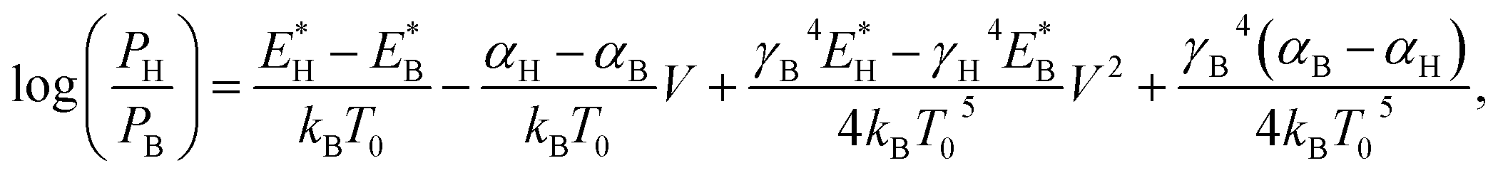
In this work, we overcome the challenging experimental hurdles encountered in the identification of the adsorption site in single-molecule junctions by combining SERS and I–V measurements with density functional theory (DFT) simulations. We illustrate the impact of this combined simultaneous optical and electrical measurements on single-molecule junctions of prototypical aminobenzenethiol (ABT) and BDT molecules. The transport properties of individual ABT and BDT molecules are measured with mechanically controllable break junctions (MCBJs) at room temperature. They feature three distinct conductance values. We find that the Raman signals, measured simultaneously with the I–V response, show distinctive features for each of the three conductance values. By combining the mode frequency from the Raman signal with the molecule–metal coupling strength from the I–V response, we can clearly identify multiple regimes, which are identified by DFT calculations as different junction adsorption sites. This identification cannot be possible by solo measurements of either SERS or I–V curves. This new combined analysis under device operating conditions enables the observation of the transition among different adsorption sites. We further apply this combined analysis to unravel the time evolution and bias-induced changes in the adsorption site, thus probing the dynamics of single-molecule junctions in realistic device conditions.
2 Methods
2.1. Simultaneous SERS and I–V curve measurements
Fig. 1a shows the photo image of the experimental setup. Single-molecule junctions were prepared using MCBJs, which offers high electrode stability and fine-tuning of the electrode spacing (Fig. S1†).2–4,24,25 The substrates used for the MCBJ technique were prepared through a series of standard nanofabrication techniques. An insulating SiO2 film (1 μm) was deposited on a polished phosphor bronze substrate of thickness t = 0.5 mm by means of sputtering. The SiO2 layer atop the phosphor-bronze substrate provides electrical insulation and limits the intensity of the Raman background scattering. Over the oxide, a polyimide film was deposited by means of spin-coating. Nanosized Au junctions, with the size of the narrowest constriction ∼300 nm × 150 nm, were prepared atop the polyimide-coated substrate using electron beam lithography and lift-off processing. Metallic layers of Cr and Au (3 nm/130 nm) were thermally evaporated onto the substrate. Subsequently, the polyimide underneath the Au junctions was removed by isotropic reactive ion etching using O2 plasma (80 W) resulting in a free-standing Au nano-electrode. Typical span lengths of the junction are in the range of ∼2 μm (see the scanning electron microscopy (SEM) image in Fig. 1b). The nano-fabricated MCBJ substrate was mounted on a three-point bending mechanism, consisting of a stacked piezo-element and two fixed counter supports. Molecules were deposited on the unbroken Au nano-bridge using self-assembly from 1 mM ABT or BDT ethanol solution. In the present study, we first prepared a Au atomic junction having a conductance of 3G0 by controlling the separation of the electrodes. The Au atomic junction spontaneously broke as a result of thermal motion of Au atoms (self-breaking).26 This sequential process of breaking of the Au atomic junction and formation and breaking of the single-molecule junction was monitored by simultaneous SERS and I–V curve measurements. The electrical measurements were performed using a Keithley 428 programmable amplifier. The SERS signals were collected using a NanoFinder30 Raman microprobe (Tokyo Instruments) with a near-infrared laser (λex = 785 nm, 5 mW at the sample surface) as an excitation light. The laser beam was focused onto the molecular junctions using an objective lens with 50× magnification and 0.50 numerical aperture. The irradiated area of the substrate was ∼1 μm2. Once the irradiation area is setup, no further adjustments in the laser position are required during the self-breaking process. The conductance of the junction was continuously measured during SERS measurements. The acquisition of each Raman spectrum took 960 ms. After the measurement of SERS, the bias voltage was swept from +1 V to −1 V within 5 ms to get the I–V curve.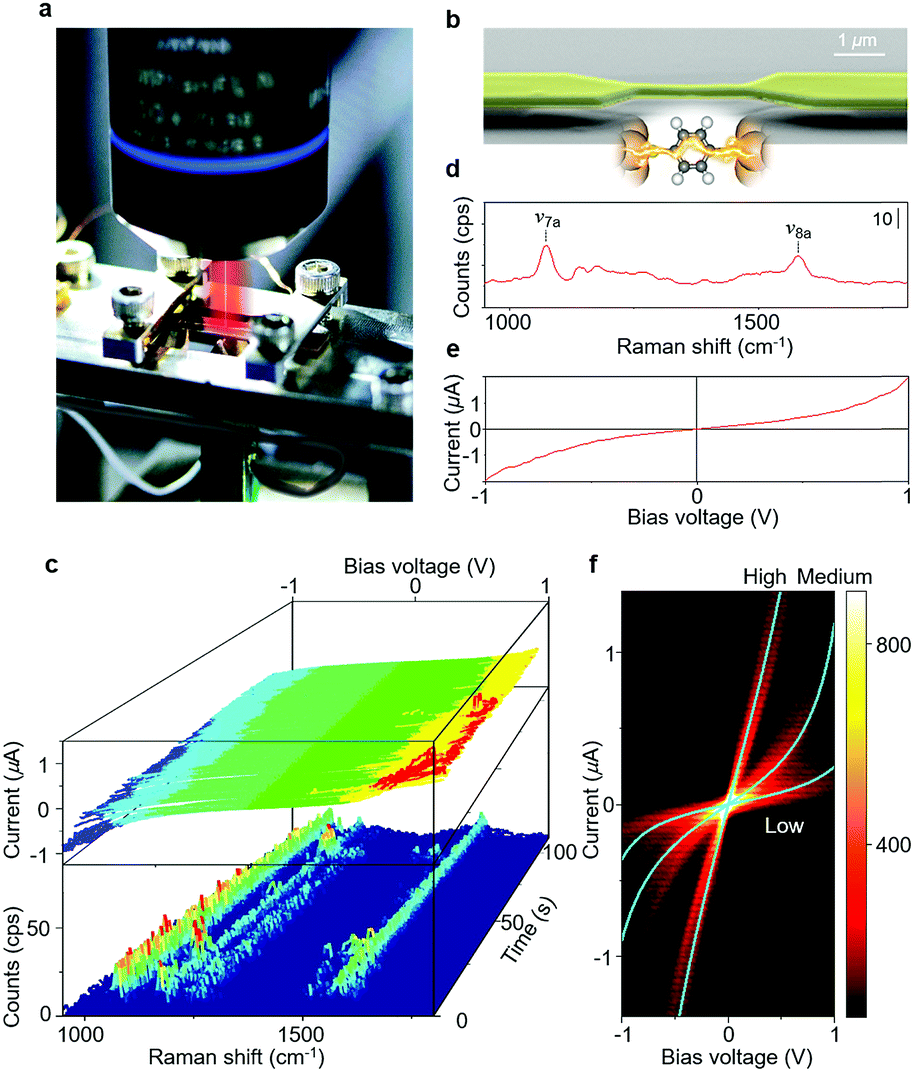 | ||
| Fig. 1 (a) Photo image of the experimental setup. (b) SEM image of the freestanding Au nano-bridge. (c) Time series of current–voltage (I–V) curves and SERS spectra of the ABT single-molecule junction. The bias voltage is 0.1 V during the SERS measurement. Example of the (d) SERS spectrum and (e) I–V curve of aminobenzenethiol (ABT) single-molecule junctions. The 1060 and 1560 cm−1 modes correspond to the C–S stretching (ν7a) and the C–C bond stretching mode (ν8a), respectively. The SERS spectrum was generated by averaging 10 samples and smoothing the operation. (f) I–V histogram of a single ABT molecular junction constructed from 1567 samples. Three statistically highly probable nonlinear curves (H, M and L) are observed. | ||
2.2. Calculation of vibrational and electron transport properties
The electronic and vibrational properties of the single-molecule junctions were calculated using ab initio methods based on the DFT-NEGF formalism.27,28 Exchange–correlation was described using the semi-local GGA approximation in the PBE implementation.29 A local-orbital basis set was employed, consisting of a double-zeta polarized basis for molecular atoms and a single-zeta polarized basis for Au atoms. The amine-gold link was modeled using three Au atoms since it is known that amine groups bind selectively to undercoordinated Au structures.7 For the thiolate-gold link, we considered structures terminating in one, two, or three Au atoms, which relaxed to atop, bridge or hollow geometries, respectively. Structures containing ABT or BDT were placed between fcc Au(111) layers, each of which contained 16 atoms. Junction structures were optimized by relaxing the molecular and Au tip motifs until the Hellmann–Feynman forces on these atoms were less than 0.02 eV Å−1. The vertical inter-electrode separation was optimized. Subsequent transport calculations were performed at optimized geometries by adding additional Au(111) layers. 5 × 5 × 1 and 15 × 15 × 1 Monkhorst–Pack grids were used for calculating the electronic structure and transmission spectra, respectively. Vibrational properties were calculated within the classical force-constant approximation using a 5 × 5 × 1 Monkhorst–Pack grid.3 Results and discussion
A strong Raman signal is only observed when the excitation laser is focused on the nano-gap between Au electrodes (Fig. S2†). Although molecules are adsorbed on the flat part of the Au electrodes, no Raman signal is detected from this. Raman scattering intensity is maximum when the incident light is polarized parallel to the junction axis. These position and polarization dependence results indicate that the Raman signal is due to the localized surface plasmon excitation of the Au nano-electrodes, and molecules between the Au electrodes are selectively observed.30 The Raman signal is seen to be correlated with junction conductance. A strong SERS signal is observed when the conductance is around 0.01G0 (2e2/h), in agreement with previously reported single molecule conductance values of BDT and ABT31,32 (Fig. S3,† see below for a discussion of BDT conductance values). The close agreement between the conductance value of the junctions where the Raman signal is most enhanced and those of the single-molecule junction supports the single molecule origin of the observed SERS signals.Fig. 1c shows an example of the time evolution of the SERS and I–V curves in the single-molecule junction regime (Fig. S4†). The SERS spectra (Fig. 1d) observed in the single-molecule junction regime show two distinct Raman bands, which are assigned to a C–S stretching mode (∼1060 cm−1, ν7a) and a C–C stretching mode (∼1560 cm−1, ν8a).33 The appearance of Raman modes characteristic of ABT indicates the presence of this molecule in the gap.34 Dimerization reactions have been reported for ABT and BDT molecules on Au nano-structures.35,36 The absence of 1380 cm−1 and 1430 cm−1 peaks corresponding to the ABT dimer and the 485 cm−1 peak corresponding to the BDT dimer indicates that the dimerization reaction does not take place at the junction under the current experimental conditions. We used a dilute ABT and BDT solution, and thus, the coverage of the molecules on the surface of the Au electrode is low. The distance between individual molecules would be too large to favour the dimerization reaction. When we use a solution of higher ABT concentration, the dimerization reaction takes place for the single-molecule junction (Fig. S5†). The non-linear I–V curve (Fig. 1e) also indicates the bridging of single molecules, as detailed below. The I–V curves of the ABT single-molecule junctions are overplotted without any data selection in Fig. 1f, showing three statistically highly probable states. We call these three states high (H), medium (M) and low (L) conductance states. The conductance profile of ABT and BDT is not significantly affected by light irradiation.
3.1. Identification of molecular adsorption sites
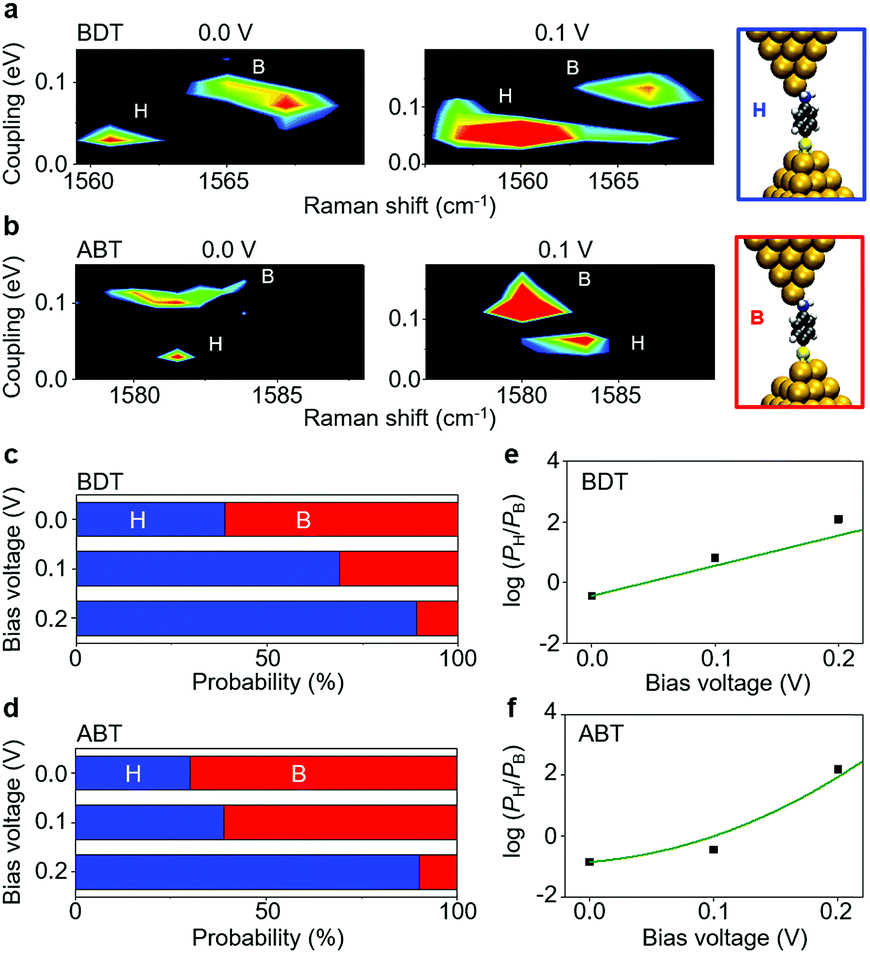
A comparison between SERS and electrical measurements reveals that the SERS signal is only observed for the H and M states. This is explained by the chemical effect, which is one of the enhancement mechanisms of SERS. The main source of the chemical effect is the charge transfer resonance taking place between metal states near the Fermi level and molecular electronic states.37 This charge transfer resonance effectively occurs when the strength of the metal–molecule interaction is strong (Fig. S7†). The strength of the metal–molecule interaction is larger for the H and M states, compared with the L state, which explains that the SERS signal is only observed for the H and M states. More importantly, we found that the H and M states exhibit different Raman shifts.Fig. 2 shows results for ABT and BDT, the two dimensional mapping of the electronic coupling Γ and the Raman shift of the mode ν8a (ring C–C stretching) for the SERS active samples i.e. samples for which the mode ν8 displays over 10 counts per second. Metal–molecule electronic coupling Γ leads to the broadening of molecular levels and is thus sensitive to the interface structure of the single-molecule junction.10 In the present experimental study, the value of Γ is obtained by fitting the I–V responses to a single-level tunneling transport model (Fig. S6†). In the mapping of Fig. 2, we can clearly observe two intense regions corresponding to H and M states, and a clear boundary between them, for both BDT and ABT. For ABT, the state M extends around ν = 1582 cm−1 and Γ = 0.064 eV (conductance G = 4.9 × 10⁻³G0), and the state H extends around ν = 1580 cm−1 and Γ = 0.14 eV (G = 3.2 × 10⁻²G0: see Table 1). The energy of mode ν8a for the conducting state H is lower than that for M. For BDT, the state M extends around ν = 1560 cm−1 and Γ = 0.062 eV (G = 3.4 × 10⁻³G0), and the state H extends around ν = 1567 cm−1 and Γ = 0.12 eV (G = 2.4 × 10⁻²G0). Each distribution of Γ or ν alone can be fitted by two Gaussian functions with different positions of the peaks, indicating the existence of two states with different Γ or ν. However, the two states overlap, and their boundary in one-variable histograms is not clear. In contrast, states can be unambiguously assigned to either H or M regimes from two-variable Γ–ν plots constructed from simultaneous SERS and I–V data. Thus, the combination of both techniques makes well-defined characterization of different junction regimes possible (ESI S7†).
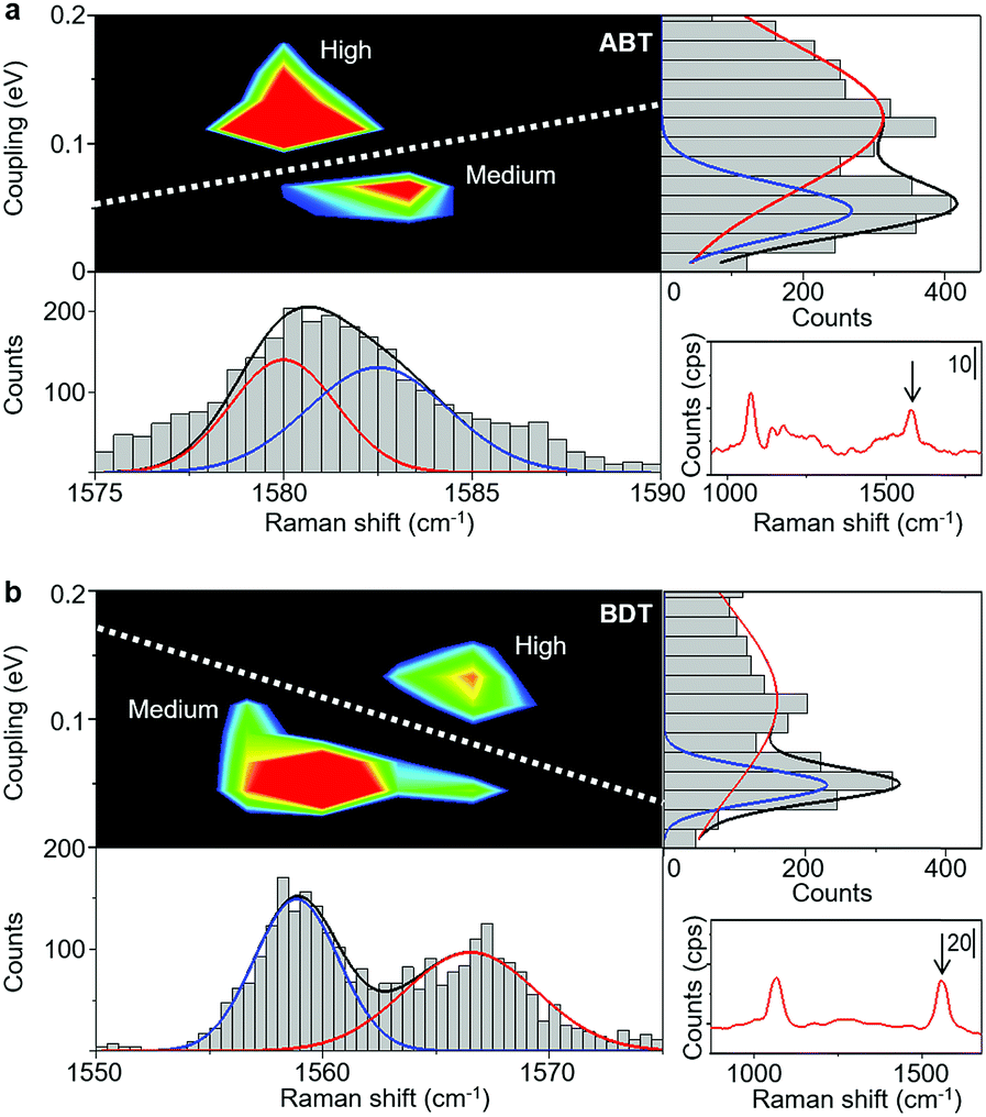 | ||
Fig. 2 (a) Two dimensional Γ-Raman shift (ν![[thin space (1/6-em)]](https://www.rsc.org/images/entities/char_2009.gif) :ν8a mode) histogram of ABT single-molecule junctions constructed from 3792 samples. The bias voltage is 0.1 V during the SERS measurement. Two regions (high and medium) with a large number of counts are separated by the white dashed line. The M region extends around ν = 1582 cm−1 and Γ = 0.064 eV, and the H state extends around ν = 1580 cm−1 and Γ = 0.14 eV. One dimensional Γ and ν histograms are shown to the right and under the 2D histogram. Red and blue lines represent the distributions of H and M states, respectively. While the distributions of H and M states overlap in the 1D histogram, both states are clearly distinguishable in the 2D Γ–ν histogram. (b) Corresponding 2D Γ–ν histogram of BDT single-molecule junctions at a bias voltage of 0.1 V constructed from 2038 samples. Two statistically highly probable regions (M: ν = 1560 cm−1 and Γ = 0.062 eV; H: ν = 1567 cm−1 and Γ = 0.12 eV) are clearly visible. :ν8a mode) histogram of ABT single-molecule junctions constructed from 3792 samples. The bias voltage is 0.1 V during the SERS measurement. Two regions (high and medium) with a large number of counts are separated by the white dashed line. The M region extends around ν = 1582 cm−1 and Γ = 0.064 eV, and the H state extends around ν = 1580 cm−1 and Γ = 0.14 eV. One dimensional Γ and ν histograms are shown to the right and under the 2D histogram. Red and blue lines represent the distributions of H and M states, respectively. While the distributions of H and M states overlap in the 1D histogram, both states are clearly distinguishable in the 2D Γ–ν histogram. (b) Corresponding 2D Γ–ν histogram of BDT single-molecule junctions at a bias voltage of 0.1 V constructed from 2038 samples. Two statistically highly probable regions (M: ν = 1560 cm−1 and Γ = 0.062 eV; H: ν = 1567 cm−1 and Γ = 0.12 eV) are clearly visible. | ||
:ν8a mode) for ABT and BDT single-molecule junctions. The G and Γ values in the parentheses are scaled by the values for the bridge (high conductance) states. The ν values in the parentheses are shown relative to the frequency of the bridge (high conductance) states. No SERS signal is observed for the atop (low conductance) state
| G (G0) | Assignment | Γ (eV) | Vib. (cm−1) | |||||
|---|---|---|---|---|---|---|---|---|
| Exp. | Calc. | Exp. | Calc. | Exp. | Calc. | |||
| ABT | High | 3.2 × 10⁻² (1) | 3.5 × 10⁻² (1) | Bridge | 0.14 (1) | 0.95 (1) | 1580 (0) | 1604 (0) |
| Medium | 4.9 × 10⁻³ (0.15) | 6.6 × 10⁻³ (0.19) | Hollow | 0.064 (0.46) | 0.38 (0.38) | 1582 (2) | 1607 (3) | |
| Low | 1.9 × 10⁻³ (0.06) | 5.2 × 10⁻³ (0.15) | Atop | 0.031 (0.22) | 0.21 (0.22) | |||
| BDT | High | 2.4 × 10⁻² (1) | 2.9 × 10⁻² (1) | Bridge | 0.12 (1) | 0.67 (1) | 1567 (0) | 1572 (0) |
| Medium | 3.4 × 10⁻³ (0.14) | 4.5 × 10⁻³ (0.16) | Hollow | 0.06 (0.52) | 0.28 (0.42) | 1560 (−7) | 1561 (−11) | |
| Low | 3.9 × 10⁻⁴ (0.02) | 2.1 × 10⁻³ (0.07) | Atop | 0.01 (0.10) | 0.11 (0.16) | |||
DFT-based simulations of single molecule electron transport characteristics and vibrational properties quantify the sensitive role played by the molecular adsorption site and identify the Γ and ν regimes as corresponding to different metal–molecule configurations. We investigated different structures for the metal–molecule contacts (ESI S8†). We found that the number of layers comprising the tip did not induce major changes in the calculated conductance, which instead is strongly influenced by the tip-molecule contact. For the amine bond in ABT, a trimer tip motif is considered since other undercoordinated Au structures7 resulted in small changes in conductance. To model the S–Au contact we consider three possible motifs, consisting of one, two or three Au adatoms (relaxed to atop, bridge or hollow geometries, respectively). For BDT, the possible combinations of these motifs on either electrode are considered.
The dependence of electron transmission and vibrational properties on the atomistic details of the metal–molecule interface allows us to establish a relationship via the tip structure between the softening of C–C vibrational frequencies and conductance. We discuss the conducting and vibrational properties of ABT (analysis of BDT is given in ESI S8†). Fig. 3a shows the C–C bond stretching mode (ν8a) of ABT for the different junction structures. Transmission calculations of ABT yield a scenario where the conductance is dominated by the highest occupied molecular orbital (HOMO). The real-space representation of the scattering state at the Fermi energy, responsible for low-bias transmission, is shown in Fig. 3b. The nodal pattern of the scattering states resembles that of the HOMO of the isolated molecule. The width and position of this HOMO-derived resonance change with the S–Au binding. Across the different tip motifs, the results for calculated conductance G show a trend which is also seen in the electronic coupling Γ (Fig. 3c). Specifically, both the conductance G and the HOMO peak width Γ decrease when going from bridge to hollow to atop structures. This trend in conductance seen in the calculations arises from the different hybridization of the S atom with the Au atom(s) which constitute the tip. It is well known that DFT calculations inherently overestimate the conductance due to errors in the position of frontier molecular orbitals,38,39 Here the DFT-based conductance values of ABT and BDT were corrected by taking into account alignment errors at the junction. For each structure, the position of the HOMO-derived resonance was rigidly shifted and the conductance was calculated within a Lorentzian model. The magnitude of each shift is the sum of two contributions of opposite sign: (i) a self-energy correction to the ionization level of the isolated molecule, (ii) a term due to screening by the metal surfaces (ESI S8†).40
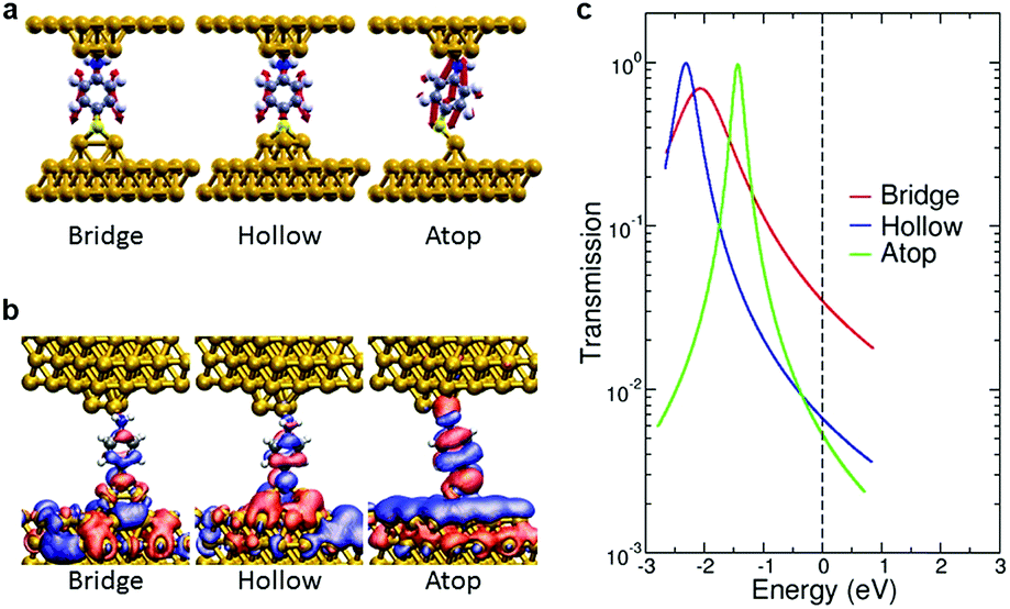 | ||
| Fig. 3 (a) Vibrational modes of ABT in the different binding configurations. (b) Transmission eigenchannels of ABT at the Fermi energy. (c) Transmission spectra of ABT after corrections to DFT resonance positions have been taken into account. | ||
Conductance values resulting from these shifts are smaller than those predicted by DFT-based calculations. This post-DFT analysis is necessary to achieve good agreement with measured conductance values and to reproduce the experimental trend. Table 1 compares the measured and calculated electrical and optical properties of ABT and BDT for the conductance states considered. Although the calculated conductance values still overestimate measurements, there is very good agreement in the ratios scaled to the largest value. For the L state we discuss conductance and resonance broadening alone due to the lack of vibrational information. The good match in conductance, resonance broadening, and vibrational frequency trends suggests that the conducting state probed experimentally is the one described in the simulations. For BDT junctions, combinations of different binding motifs introduce multiple conductance states. This leads to a range of calculated conductance values (ESI S8†).
Early studies compared the measured and calculated values of conductance alone. Subsequently, vibrational spectroscopy techniques provided further details. In the present work, we could unambiguously identify the molecular adsorption site through the combination of SERS, I–V measurements, and DFT simulations. Thiol-bonded conducting junctions, particularly BDT, have been examined in the literature from experiments,8,31,41 calculations,42,43 and joint studies,9,11,31,44 where the large discrepancies in conductance have been subject to debate. Although Xiao et al. reported a single conductance state (0.011G0),31 most studies have reported multiple conductance states8,11,41,44 or continuous extended conductance states.42,43 Tsutsui et al. showed a high (0.1G0) and a low (0.01G0) conductance state and argued that these different conductance states were caused by the positions of the adsorbed molecule. They concluded that the high and the low conductance relate to the hollow and top sites, respectively.41 Leary et al. observed two conductance peaks (2 × 10⁻² and 3 × 10⁻⁴G0) for BDT and proposed the formation of oligomeric Au-(RS)2 units at the molecule–metal interface to explain the low-conductance feature based on conductance and plateau length analysis and an atop geometry for the higher conductance peak.11 A combination of several experimental techniques thus seems essential in aiding the characterization of the junction geometry of this nontrivial system. Kim et al. employed conductance and IETS measurements and assigned low (6 × 10⁻⁴G0) and high conductance states (0.5G0) to binding via top and hollow sites, respectively.8 Karimi et al. showed that low (2.5 × 10⁻²G0) and high conductance states (0.2G0) correspond to hollow and top sites, respectively, based on experimental (conductance IETS and shot noise) and theoretical investigations.9 Komoto et al. reported three conductance states, low (3.1 × 10⁻⁴G0), medium (1.7 × 10⁻³G0) and high (3.7 × 10⁻²G0), from conductance and I–V response, and interpreted them as binding via top, hollow, and bridge sites, respectively, with the aid of theoretical calculations.44 It is worth highlighting that atop or hollow binding configurations are ascribed in the literature to high and low experimental conductance values, which can differ by one or more orders of magnitude. We note that we consider single molecule junctions having conductance values below 0.05G0, thus excluding from our study structures where the phenyl ring interacts directly with the Au electrodes.9 The observed results and the assignment given in Ref (44) agree with the present study. As for the formation of Au-thiolate molecular oligomers, such elongated junction structures were not found in our results, thus ruling out their role or that of metallic chains under the experimental conditions investigated.
Here, we briefly comment on the fabrication technique of the single-molecule junction. In most of the studies, the conductance of the single-molecule junction is evaluated by using the break junction technique. In the break junction process, the meta-stable atomic configuration can be formed due to the short measurement time. In contrast, we have prepared the single-molecule junction by using the self-breaking technique. In contrast with the break junction technique, the atomic configuration would change into a thermally stable configuration. Therefore, the atomic configuration and conductance values can be different from those obtained by the break junction technique.
3.2. Thermal- and voltage-induced transitions in the molecular adsorption site
Having resolved the characterization of the molecular adsorption geometry underlying the junction electrical characteristics through simultaneous SERS and I–V response and DFT simulations, we now address the dynamical fluctuations between these sites. Fig. 4 shows two examples of temporal change, from state S1 to S2, and from state S3 to S4, in conductance (G) and metal–molecule electronic coupling (Γ), determined from the I–V response, as well as from the Raman frequency (ν) for the ABT single-molecule junction. The time evolution of conductance/coupling and Raman shift was collected simultaneously. The bridge and hollow regimes are indicated in blue and red colors, respectively. A fringe region between these regimes is shown in purple color, which corresponds to structures which cannot be unambiguously identified from transport or vibrational measurements alone. In Fig. 4a the conductance of the initial state S1 is 0.018G0 and both coupling and Raman shift are in the bridge regime. In the final state of S2, the conductance has decreased to 6.7 × 10⁻³G0, and the coupling and Raman shift have changed into those of the hollow region. In Fig. 4b the conductance of the initial state S3 is 0.016G0. Since the coupling Γ is close to the boundary region, it is hard to define the adsorption site from Γ alone. In the final state S4, the conductance has changed only slightly with respect to S3 and from electron transport information alone, G and Γ, it is not possible to infer any changes in the adsorption site. In contrast, the Raman shift clearly decreases from S3 to S4 and the combined analysis unambiguously characterizes the molecular adsorption site: hollow for S3 and bridge for S4. Other examples of transition between sites are shown in ESI S9.† The present combined analysis can thus follow temporal fluctuations in conductance through changes in Γ and ν induced by changes in the molecular adsorption site, which are hardly detected by electrical or vibrational measurements alone.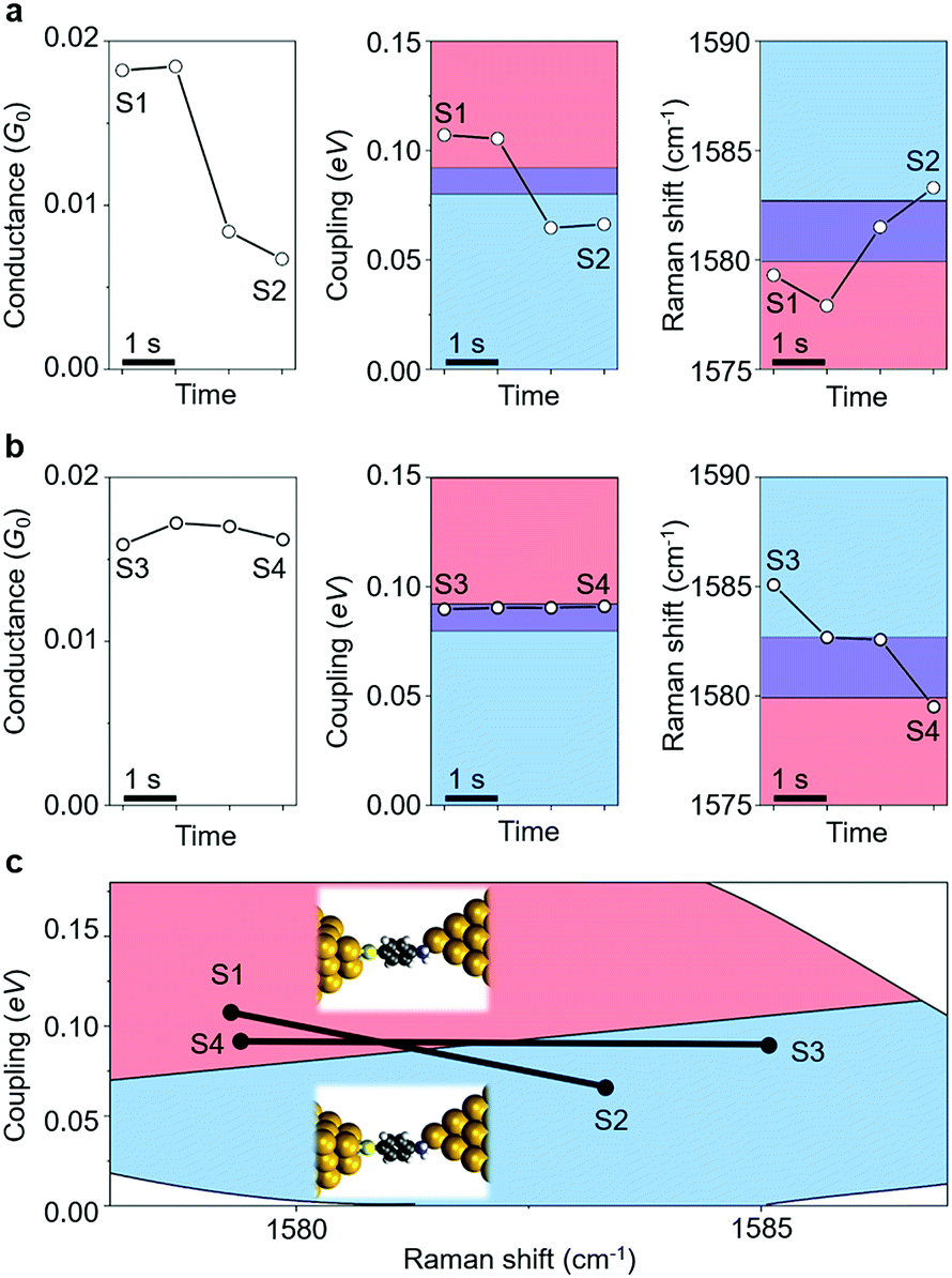 | ||
| Fig. 4 (a) Time evolution of conductance (G: left), Γ (middle) and ν (right) of the ABT single-molecule junction. Red and blue regions correspond to bridge and hollow sites, respectively. Both regimes overlap in the Γ and ν panels in the purple region. Transition is clear from both coupling and Raman shift in (a) and the transition is clear only from the Raman shift in (b). (c) Transition from the bridge to hollow sites is observed in the 2D Γ–ν mapping. G, Γ and ν are 0.018G0, 0.11 eV, and 1579 cm−1 for S1, 6.7 × 10⁻³G0, 0.066 eV, and 1583 cm−1 for S2, 0.016G0, 0.090 eV, and 1585 cm−1 for S3, and 0.016G0, 0.091 eV, and 1579 cm−1 for S4. | ||
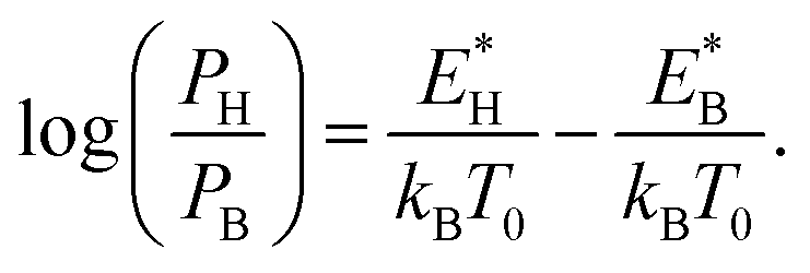
Finally, we address fluctuations in the molecular adsorption site induced by the application of a bias voltage to the single-molecule junction (details are given in ESI S10†). The 2D Γ–ν mapping of ABT and BDT single-molecule junctions is shown in Fig. 5a and b for two different bias voltages. Two regions, corresponding to bridge and hollow sites, are clearly apparent. At zero bias voltage, the upper-left region (large Γ and small ν), characteristic of a bridge site, is intense for ABT, while for BDT it is the upper-right bridge region (large Γ and large ν). As the bias is increased, the intensity of the bridge region decreases, and lower-right (ABT) and lower-left (BDT) hollow regions become intense, indicating an increase of the bridge to hollow site transitions. Fig. 5c and d show the fraction of the molecular adsorption sites obtained by the combined SERS–I–V measurements as a function of the total signal. With increasing bias voltage, the most probable adsorption site changes from the thermally stable bridge to the hollow site. It should be noticed that the bias voltage does not change the Raman shift within 1 cm−1 for the BDT single-molecule junction. The observed change in the Γ–ν mapping is actually caused by the adsorption site change.
 | ||
| Fig. 5 The 2D Γ–ν histograms for (a) BDT and (b) ABT single-molecule junctions at different bias voltages. The histograms are constructed from 3085 (0.0 V) and 2038 (0.1 V) samples for BDT and 1355 (0.0 V) and 3792 (0.1 V) samples for ABT. Distribution of molecular adsorption sites identified by the Γ–ν combination analysis for the (c) BDT and (d) ABT single-molecule junctions at different bias voltages of 0, 0.1 and 0.2 V. (e and f) Bias dependence of the site populations; theory (solid lines) and measured values (circles) for (e) BDT and (f) ABT. The probability of the site population is denoted as PH and PB for the hollow and bridge adsorption. | ||
In order to analyse the distinct bias-voltage dependence of the populations of the bridge (PB) and hollow (PH) sites, we examine a simple theoretical model based on kinetic theory and non-equilibrium electric transport theory. When a transition between the adsorption structures is described by one-step kinetics, the transition probability from the bridge (B) to the hollow (H) site may be written as  The reverse transition is also expressed as
 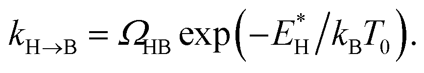 ΩBH(HB) represents the attempt frequency from B to H (H to B) sites and we have set ΩBH equal to ΩHB for simplicity. The terms E*, kB, and T0 are the activation energy, Boltzmann constant, and temperature of the junction, respectively. The ratio PH/PB satisfies the following relationship:
 | (1) |
Eqn (1) is applicable only to systems in thermal equilibrium, i.e., the applied bias must be zero. When a bias is applied, the molecular junction is in non-equilibrium. Two main effects accelerate ionic motions: local heating45,46 and current-induced force.47,48 The former is caused by the inelastic scattering of electrons and ions, while the latter consists of electric force by voltage drop and elastic scattering of electrons and ions. Though the system is not thermally equilibrated by local heating, we assume that the focused system (i.e., the adsorbed molecule) can be approximated as a quasi-equilibrium system and chemical kinetics is applicable. Then it is reasonable to introduce the effective junction temperature into the model as a function of bias V.45,49,50 In addition, the current-induced force changes the potential energy profile. Therefore, we incorporate it into E*, where we approximate E* as a linear function of V as given in ref. 51. Here, we only consider V > 0. Replacing T0 and E* in eqn (1) with their voltage-dependent functions, we obtain the relative populations as a function of applied bias:
 | (2) |
4 Conclusions
We have demonstrated an adsorption site identification technique based on an analysis combining SERS and current–voltage response measurements, with the aid of DFT calculations. When applied to two paradigmatic single-molecule junctions, this methodology distinguishes multiple molecular adsorption sites, and uncovers the origin of conductance fluctuations. In the case of ABT and BDT, conductance can vary by up to a factor 1000, a situation that hampers the development of clear, reproducible conductance signatures. The present study unambiguously monitors the changes in the molecular adsorption geometry for the first time and the changes in the population of adsorption sites as a function of time and applied voltage. Characterization and control over the molecular adsorption site remain, despite its impact on single molecule conductance, a difficult task. This highlights the creation of atomically well-defined metal–molecule interfaces as one of the next challenges towards the realization of single molecule circuits, and underscores the importance of the present methodology. Using our new technique, we can determine the adsorption site for each single-molecule junction, and thus, select the junction with a certain fixed adsorption site. By integrating the selected single-molecule junctions with a fixed adsorption site, the fluctuation of the performance of the electronic circuit should be drastically suppressed. Our work thus opens the way to studying and governing single molecule circuits.Conflicts of interest
There are no conflicts to declare.Acknowledgements
This work was financially supported by the Grants-in-Aid for Scientific Research (No. 19H04673, 19H05386, and 18H03896) from the MEXT, and JST CREST (JPMJCR18I4). E. M. and H. V acknowledge the Purkyně Fellowship program of the Czech Academy of Sciences and the Czech Science Foundation (grant number 15-19672S). Computational resources were provided by the National Grid Infrastructure MetaCentrum and the “Projects of Large Research, Development, and Innovations Infrastructures” program (CESNET LM2015042 and LM2015087).Notes and references
- A. Aviram and M. A. Ratner, Chem. Phys. Lett., 1974, 29, 277–283 CrossRef CAS
.
-
M. Kiguchi, Single-Molecule Electronics: An Introduction to Synthesis, Measurement and Theory, Springer, Singapore, 2016 Search PubMed
- H. Song, M. A. Reed and T. Lee, Adv. Mater., 2011, 23, 1583–1608 CrossRef CAS PubMed
- N. J. Tao, Nat. Nanotechnol., 2006, 1, 173–181 CrossRef CAS PubMed
- H. Song, Y. Kim, Y. H. Jang, H. Jeong, M. A. Reed and T. Lee, Nature, 2009, 462, 1039–1043 CrossRef CAS PubMed
- S. Fujii, S. Marques-Gonzalez, J. Y. Shin, H. Shinokubo, T. Masuda, T. Nishino, N. P. Arasu, H. Vazquez and M. Kiguchi, Nat. Commun., 2017, 8, 15984 CrossRef CAS PubMed
- L. Venkataraman, J. E. Klare, I. W. Tam, C. Nuckolls, M. S. Hybertsen and M. L. Steigerwald, Nano Lett., 2006, 6, 458–462 CrossRef CAS PubMed
- Y. Kim, T. Pietsch, A. Erbe, W. Belzig and E. Scheer, Nano Lett., 2011, 11, 3734–3738 CrossRef CAS PubMed
- M. A. Karimi, S. G. Bahoosh, M. Herz, R. Hayakawa, F. Pauly and E. Scheer, Nano Lett., 2016, 16, 1803–1807 CrossRef CAS PubMed
- Y. Isshiki, S. Fujii, T. Nishino and M. Kiguchi, J. Am. Chem. Soc., 2018, 140, 3760–3767 CrossRef CAS PubMed
- E. Leary, L. A. Zotti, D. Miguel, I. R. Marquez, L. Palomino-Ruiz, J. M. Cuerva, G. Rubio-Bollinger, M. T. Gonzalez and N. Agrait, J. Phys. Chem. C, 2018, 122, 3211–3218 CrossRef CAS
- S. Terada, T. Yokoyama, M. Sakano, A. Imanishi, Y. Kitajima, M. Kiguchi, Y. Okamoto and T. Ohta, Surf. Sci., 1998, 414, 107–117 CrossRef CAS
- W. Haiss, C. S. Wang, I. Grace, A. S. Batsanov, D. J. Schiffrin, S. J. Higgins, M. R. Bryce, C. J. Lambert and R. J. Nichols, Nat. Mater., 2006, 5, 995–1002 CrossRef CAS PubMed
- J. Yoshinobu, N. Takagi and M. Kawai, Chem. Phys. Lett., 1993, 211, 48–52 CrossRef CAS
- J. Hihath, C. R. Arroyo, G. Rubio-Bollinger, N. Tao and N. Agrait, Nano Lett., 2008, 8, 1673–1678 CrossRef PubMed
- S. Nie, Science, 1997, 275, 1102–1106 CrossRef CAS PubMed
- G. C. Phan-Quang, H. K. Lee, H. W. Teng, C. S. L. Koh, B. Q. Yim, E. K. M. Tan, W. L. Tok, I. Y. Phang and X. Y. Ling, Angew. Chem., Int. Ed., 2018, 57, 5792–5796 CrossRef CAS PubMed
- Z. Ioffe, T. Shamai, A. Ophir, G. Noy, I. Yutsis, K. Kfir, O. Cheshnovsky and Y. Selzer, Nat. Nanotechnol., 2008, 3, 727–732 CrossRef CAS PubMed
- Z. Liu, S. Y. Ding, Z. B. Chen, X. Wang, J. H. Tian, J. R. Anema, X. S. Zhou, D. Y. Wu, B. W. Mao, X. Xu, B. Ren and Z. Q. Tian, Nat. Commun., 2011, 2, 305 CrossRef PubMed
- D. R. Ward, D. A. Corley, J. M. Tour and D. Natelson, Nat. Nanotechnol., 2011, 6, 33–38 CrossRef CAS PubMed
- H. Bi, C. A. Palma, Y. X. Gong, P. Hasch, M. Elbing, M. Mayor, J. Reichert and J. V. Barth, J. Am. Chem. Soc., 2018, 140, 4835–4840 CrossRef CAS PubMed
- S. Kaneko, D. Murai, S. Marques-Gonzalez, H. Nakamura, Y. Komoto, S. Fujii, T. Nishino, K. Ikeda, K. Tsukagoshi and M. Kiguchi, J. Am. Chem. Soc., 2016, 138, 1294–1300 CrossRef CAS PubMed
- L. A. Zotti, T. Kirchner, J. C. Cuevas, F. Pauly, T. Huhn, E. Scheer and A. Erbe, Small, 2010, 6, 1529–1535 CrossRef CAS PubMed
- M. A. Reed, C. Zhou, C. J. Muller, T. P. Burgin and J. M. Tour, Science, 1997, 278, 252–254 CrossRef CAS
- C. Kergueris, J. P. Bourgoin, S. Palacin, D. Esteve, C. Urbina, M. Magoga and C. Joachim, Phys. Rev. B: Condens. Matter Mater. Phys., 1999, 59, 12505–12513 CrossRef CAS
- M. Tsutsui, K. Shoji, M. Taniguchi and T. Kawai, Nano Lett., 2008, 8, 345–349 CrossRef CAS PubMed
- J. M. Soler, E. Artacho, J. D. Gale, A. Garcia, J. Junquera, P. Ordejon and D. Sanchez-Portal, J. Phys.: Condens. Matter, 2002, 14, 2745–2779 CrossRef CAS
- M. Brandbyge, J. L. Mozos, P. Ordejon, J. Taylor and K. Stokbro, Phys. Rev. B: Condens. Matter Mater. Phys., 2002, 65, 165401 CrossRef
- J. P. Perdew, K. Burke and M. Ernzerhof, Phys. Rev. Lett., 1996, 77, 3865–3868 CrossRef CAS PubMed
- J. H. Tian, B. Liu, X. Li, Z. L. Yang, B. Ren, S. T. Wu, N. Tao and Z. Q. Tian, J. Am. Chem. Soc., 2006, 128, 14748–14749 CrossRef CAS PubMed
- X. Y. Xiao, B. Q. Xu and N. J. Tao, Nano Lett., 2004, 4, 267–271 CrossRef CAS
- Y. Komoto, S. Fujii and M. Kiguchi, Adv. Nat. Sci.: Nanosci. Nanotechnol., 2017, 8, 025007 Search PubMed
- M. Osawa, N. Matsuda, K. Yoshii and I. Uchida, J. Phys. Chem., 1994, 98, 12702–12707 CrossRef CAS
- P. Xu, L. L. Kang, N. H. Mack, K. S. Schanze, X. J. Han and H. L. Wang, Sci. Rep., 2013, 3, 2997 CrossRef PubMed
- J. T. Zheng, J. Y. Liu, Y. J. Zhuo, R. H. Li, X. Jin, Y. Yang, Z. B. Chen, J. Shi, Z. Y. Xiao, W. J. Hong and Z. Q. Tian, Chem. Sci., 2018, 9, 5033–5038 RSC
- Y. F. Huang, H. P. Zhu, G. K. Liu, D. Y. Wu, B. Ren and Z. Q. Tian, J. Am. Chem. Soc., 2010, 132, 9244–9246 CrossRef CAS PubMed
- J. R. Lombardi, R. L. Birke, T. Lu and J. Xu, J. Chem. Phys., 1986, 84, 4174–4180 CrossRef CAS
- J. B. Neaton, M. S. Hybertsen and S. G. Louie, Phys.
Rev. Lett., 2006, 97, 216405 CrossRef CAS PubMed
- F. Flores, J. Ortega and H. Vazquez, Phys. Chem. Chem. Phys., 2009, 11, 8658–8675 RSC
- S. Y. Quek, L. Venkataraman, H. J. Choi, S. G. Louie, M. S. Hybertsen and J. B. Neaton, Nano Lett., 2007, 7, 3477–3482 CrossRef CAS PubMed
- M. Tsutsui, Y. Teramae, S. Kurokawa and A. Sakai, Appl. Phys. Lett., 2006, 89, 163111 CrossRef
- N. Sergueev, L. Tsetseris, K. Varga and S. Pantelides, Phys. Rev. B: Condens. Matter Mater. Phys., 2010, 82, 073106 CrossRef
- R. B. Pontes, A. R. Rocha, S. Sanvito, A. Fazzio and A. J. da Silva, ACS Nano, 2011, 5, 795–804 CrossRef CAS PubMed
- Y. Komoto, S. Fujii, H. Nakamura, T. Tada, T. Nishino and M. Kiguchi, Sci. Rep., 2016, 6, 26606 CrossRef CAS PubMed
- T. N. Todorov, Philos. Mag. B, 1998, 77, 965–973 CrossRef CAS
- J.-T. Lü, M. Brandbyge, P. Hedegård, T. N. Todorov and D. Dundas, Phys. Rev. B: Condens. Matter Mater. Phys., 2012, 85, 245444 CrossRef
- T. N. Todorov, J. Hoekstra and A. P. Sutton, Philos. Mag. B, 2000, 80, 421–455 CrossRef CAS
- R. X. Zhang, I. Rungger, S. Sanvito and S. M. Hou, Phys. Rev. B: Condens. Matter Mater. Phys., 2011, 84, 085445 CrossRef
- Z. Huang, F. Chen, P. A. Bennett and N. Tao, J. Am. Chem. Soc., 2007, 129, 13225–13231 CrossRef CAS PubMed
- M. Tsutsui, M. Taniguchi and T. Kawai, Nano Lett., 2008, 8, 3293–3297 CrossRef CAS PubMed
-
M. Di Ventra, Electrical Transport in Nanoscale Systems, Cambridge Univ. Press, Cambridge, 2008 Search PubMed
Footnote |
| † Electronic supplementary information (ESI) available. See DOI: 10.1039/c9sc00701f |
| This journal is © The Royal Society of Chemistry 2019 |