
 Open Access Article
 This Open Access Article is licensed under a Creative Commons Attribution-Non Commercial 3.0 Unported Licence
Efficient photoredox conversion of alcohol to aldehyde and H2 by heterointerface engineering of bimetal–semiconductor hybrids†
Chuang
Han
ab,
Zi-Rong
Tang
 b,
Junxue
Liu
c,
Shengye
Jin
*c and
Yi-Jun
Xu
*ab
b,
Junxue
Liu
c,
Shengye
Jin
*c and
Yi-Jun
Xu
*ab
aState Key Laboratory of Photocatalysis on Energy and Environment, College of Chemistry, Fuzhou University, Fuzhou, 350116, China. E-mail: yjxu@fzu.edu.cn
bCollege of Chemistry, Fuzhou University, New Campus, Fuzhou, 350116, China
cState Key Laboratory of Molecular Reaction Dynamics, Dalian Institute of Chemical Physics, Chinese Academy of Sciences, Dalian, Liaoning 116023, China. E-mail: sjin@dicp.ac.cn
First published on 7th February 2019
Abstract
Controllable and precise design of bimetal– or multimetal–semiconductor nanostructures with efficient light absorption, charge separation and utilization is strongly desired for photoredox catalysis applications in solar energy conversion. Taking advantage of Au nanorods, Pt nanoparticles, and CdS as the plasmonic metal, nonplasmonic co-catalyst and semiconductor respectively, we report a steerable approach to engineer the heterointerface of bimetal–semiconductor hybrids. We show that the ingredient composition and spatial distribution between the bimetal and semiconductor significantly influence the redox catalytic activity. CdS deposited anisotropic Pt-tipped Au nanorods, which feature improved light absorption, structure-enhanced electric field distribution and spatially regulated multichannel charge transfer, show distinctly higher photoactivity than blank CdS and other metal–CdS hybrids for simultaneous H2 and value-added aldehyde production from one redox cycle.
Introduction
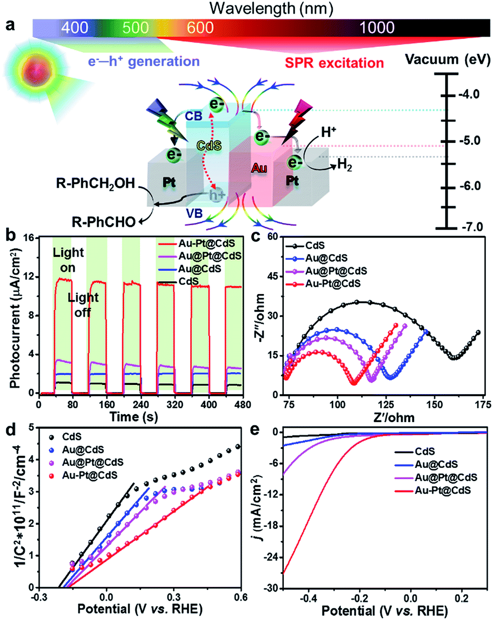
Harvesting solar energy to drive artificial photosynthesis for the production of value-added chemicals and renewable energy is a promising strategy to solve the growing worldwide energy crisis.1–5 However, the solar-to-chemical conversion efficiency of semiconductors is often limited by their finite light absorption and/or slow charge separation rates and reaction kinetics.6–10 Integrating different functional materials into a single hybrid structure with precise design holds great promise for constructing efficient composite photocatalysts owing to the synergistic properties induced by the interactions between these components in an integrative ensemble.5,11–16Bimetallic nanostructures, coupling a surface plasmon resonance (SPR, Scheme S1†) functionality with an efficient co-catalytic effect, could be an ideal candidate to simultaneously modulate the photoabsorption and steer the multichannel charge separation/transfer and reaction kinetics of semiconductors.17–21 The design of effective bimetal–semiconductor composite photocatalysts requires the rational understanding of the structural design principle, because the randomly hybridizing counterparts would often shield the SPR intensity and local electric field of the plasmonic metal or weaken the net photoabsorption of the semiconductor.22–25 In addition, recent research has predominantly focused on charge separation and transfer mainly occurring at the plasmonic metal domains (i.e., SPR-induced sensitization effect),25–27 and the quantum efficiency over such systems is still relatively low in contrast to those by semiconductor photoexcitation. To obtain high photocatalytic activity, the structural design of special composite catalysts to synergistically utilize the SPR enhancement mechanism and band-gap photoexcitation of semiconductors is desirable.28,29 However, thus far, it is still unclear how the composition and structural arrangement of plasmonic–nonplasmonic bimetal hybrids comprehensively affect their interactions with the semiconductor and the subsequent band alignment, charge transfer dynamics, local electric field distribution and redox catalysis performance.
Herein, we report a controllable way to design bimetal–semiconductor hybrids with different heterointerfaces for progressively improved redox catalysis conversion of alcohol to H2 and aldehyde under visible-near-infrared (Vis-NIR) light irradiation. Au nanorods (NRs) and Pt nanoparticles (NPs) are promising metallic nanocrystal platforms for fabricating metal–semiconductor hybrids due to their tunable longitudinal-SPR absorption in the near-infrared (NIR) region and high efficiency for catalytic proton reduction reaction, respectively.13,30–34 In this regard, we chose Au NRs and Pt NPs to form the plasmonic bimetal component. CdS, a well-known visible (Vis) light responsive photocatalyst with a direct band-gap of around 2.4 eV,8,35–38 is chosen as the semiconductor component. Integrating the co-catalytic factor with semiconductor photoexcitation and SPR resonance modes in different optical response regions by the rational assembly of nonplasmonic Pt NPs and semiconductor CdS on the surface of Au NRs can provide the spatial transfer multichannel for electrons and boost the local electric field, promoting the generation and migration of electron–hole charge carriers. As a result, the CdS deposited anisotropic Pt-tipped Au NRs (Au–Pt@CdS), which features the multiple metal–semiconductor and metal–metal heterojunctions, exhibits distinctly higher photoactivity than blank CdS and other metal–CdS hybrid counterparts for photocatalytic conversion of alcohol to aldehyde and H2 by simultaneous utilization of photogenerated holes and electrons in one redox cycle. Resorting to electric field simulations, transient absorption spectroscopy and multiple control experiments, it is demonstrated that the redox photoactivity is highly dependent on the ingredient composition and spatial distribution of the metal components because they play a significant role in affecting multiple electron transfer pathways and local electric field enhancement.
Results and discussion
The fabrication process is based on progressively seed-mediated growth, as illustrated in Scheme 1. The stronger interaction between the cetyltrimethylammonium bromide (CTAB) surface-capping molecules and the side facets of Au NRs results in the higher packed density of CTAB at the sides than that at the ends of Au NRs.24,25 By taking advantage of this anisotropic surface structure, Pt NPs were firstly selectively deposited on the tips of Au NR seeds for the preparation of anisotropic Pt-tipped Au NRs (Au–Pt). The spatial distribution of Pt on the Au NR surface depends on the surface-capping molecules. Pt-covered Au NRs (Au@Pt) can be synthesized by decreasing the concentration of CTAB molecules. The Au-based NRs were subsequently used as seeds for the assembly of semiconductor CdS via a facile and controllable refluxing process. It should be noticed that our synthesis reaction is performed at a low temperature (85 °C) and in the absence of metal ion sources (e.g., Ag+ or Cu2+) as a “bridge” between Au NRs and CdS to achieve the heterogrowth,39,40 which can prevent the Au NRs from undesired reshaping in the wet-chemistry growth process.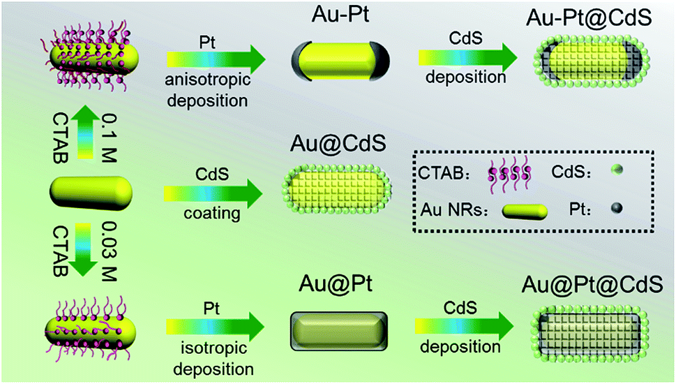 | ||
| Scheme 1 Schematic flowchart illustrating the controllable preparation of CdS deposited Pt-tipped Au NRs (Au–Pt@CdS), CdS deposited Au NRs (Au@CdS) and CdS deposited Pt-covered Au NRs (Au@Pt@CdS). | ||
The samples obtained in each growth stage were characterized using scanning electron microscopy (SEM) and transmission electron microscopy (TEM) analysis. The average diameter and length of the original Au NRs are 29.0 and 92.5 nm, respectively (Fig. 1a and S1†). After the growth of Pt on the tips of Au NRs, the smooth ends of Au NRs become gibbous, while the surface at the side of Au NRs remains almost unchanged (Fig. 1b and S2†). The average diameter at the middle of Au–Pt NRs is 29.1 nm, and the average length is increased to 114.0 nm. These results suggest that Pt tends to anisotropically deposit at the two ends of Au NRs. Fig. 1c and S3† show the morphology of Au@Pt with an average diameter of 33.2 nm and length of 107.9 nm, which are enclosed by the Pt shell.
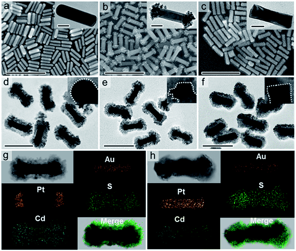 | ||
| Fig. 1 SEM images of (a) Au NRs, (b) Au–Pt, and (c) Au@Pt, scale bar, 200 nm. The insets of (a–c) show TEM images of the corresponding samples, scale bar, 20 nm. TEM images of (d) Au@CdS, (e) Au–Pt@CdS and (f) Au@Pt@CdS, scale bar, 200 nm. Elemental mapping results of (g) Au–Pt@CdS and (h) Au@Pt@CdS. | ||
The morphology information of CdS deposited Au NRs (Au@CdS), CdS deposited Pt-tipped Au NRs (Au–Pt@CdS) and CdS deposited Pt-covered Au NRs (Au@Pt@CdS) is disclosed in Fig. 1d–f and S4.† No noticeable structural deformation of Au-based seeds can be discerned after depositing CdS nanoshells, which should benefit from the mild reaction process at a low temperature. For Au@CdS, we can clearly see from Fig. 1d and S4a–c† that the Au NR core with hemispherical ends are coated with a loose and porous CdS semiconductor layer in thicknesses of 15–20 nm. TEM images of Au–Pt@CdS (Fig. 1e) and Au@Pt@CdS (Fig. 1f) indicate their similar overall shape to Au@CdS. However, the bimetal cores in Au–Pt@CdS and Au@Pt@CdS respectively show convex (Fig. S4d–f†) and bar-like (Fig. S4g–i†) shapes. Elemental mapping analysis of Au–Pt@CdS (Fig. 1g) discloses that the Pt is located at the ends of Au NRs, further confirming the tip-coated morphology of the Au–Pt core in Au–Pt@CdS. Elemental mapping study of Au@Pt@CdS indicates that the layers of Pt and CdS shells are both isotropically deposited on the entire surface of Au NRs (Fig. 1h). The morphology of blank CdS was also analyzed (Fig. S5†), suggesting that blank CdS is composed of tiny NPs.
X-ray diffraction (XRD) patterns of blank CdS and metal–CdS hybrids are shown in Fig. 2a, in which the diffraction peaks of hexagonal phase CdS (JCPDS, no. 41-1049) and cubic phase Au (JCPDS, no. 65-8601) can be well identified. The characteristic diffraction peaks of Pt are hardly observed due to their relatively low content in the composites.41 Raman spectra, as displayed in Fig. 2b, show that blank CdS exhibits Raman signals at 299 cm−1, 597 cm−1 and 890 cm−1, which are identified as characteristic peaks of the longitudinal optical (LO) phonons of the CdS phase.42 In comparison with CdS, all of these peaks are significantly intensified for metal–CdS hybrids, suggesting an enhanced light–matter interaction due to the strong electric field enhancement near the surface of plasmonic Au-based NRs.42
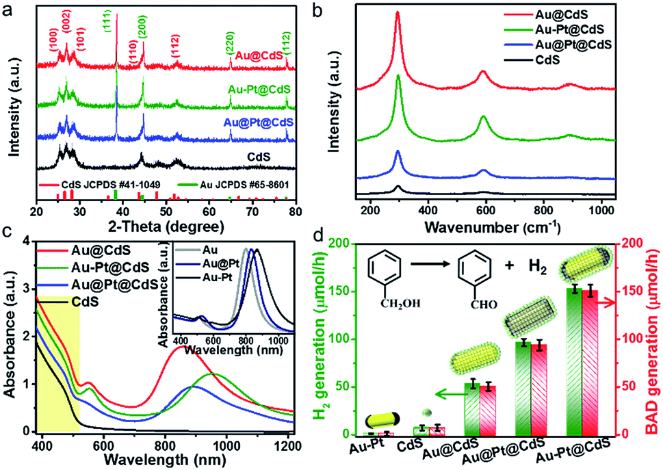 | ||
| Fig. 2 (a) XRD patterns, (b) Raman spectra and (c) absorption spectra of CdS and metal–CdS hybrids. The inset of (c) shows the normalized absorption spectra of Au, Au@Pt and Au–Pt for comparison. (d) H2 and benzaldehyde (BAD) generation rate in the photocatalytic conversion of benzyl alcohol (BA) under Vis-NIR light (λ > 420 nm) irradiation over Au–Pt, CdS and metal–CdS hybrids. The insets of (d) show the formula for photocatalytic conversion of BA and the corresponding structural models of the samples. | ||
The evolution of optical absorption spectra along with the structural variation of the samples is displayed in Fig. 2c. The raw Au NRs have two SPR absorption bands centered at 510 and 800 nm, which are respectively assigned to transverse-SPR (T-SPR) and longitudinal-SPR (L-SPR) photoabsorption (inset of Fig. 2c). After Pt is deposited on Au NRs, the L-SPR band red-shifts to 833 and 865 nm for Au@Pt and Au–Pt, respectively. In addition, the T-SPR band of Au@Pt slightly red-shifts to 527 nm, while almost no change occurs for that of Au–Pt, which is probably due to the selective deposition of Pt onto the tips of Au NRs for the Au–Pt sample.24 Both T-SPR and L-SPR bands are further red-shifted after the semiconductor CdS is grown on Au@Pt and Au–Pt, resulting from the increase of the surrounding dielectric constant.31,43 The blank CdS and metal–CdS hybrids disclose a similar optical absorption threshold located at 520 nm, which corresponds to the optical band-gap of about 2.4 eV in the pristine CdS semiconductor. However, the absorption of metal–CdS hybrids is higher than that of blank CdS throughout the whole Vis to NIR region due to the contribution from the SPR absorption of Au-based NRs.36,43
We tested the samples as dual-function photocatalysts for the conversion of benzyl alcohol (BA) to H2 and benzaldehyde (BAD) under Vis-NIR light (λ > 420 nm, Fig. S6†) irradiation. We initially studied the effects of the proportion of different components on the photoactivity and determined the sample with optimal photoactivity, as shown in Fig. S7a–c.† The direct photoactivity comparison with the H2 and BAD production rates over the samples with the optimal proportion of components is shown in Fig. 2d. Notably, the molar ratio of the reduction product (H2) and oxidation product (BAD) is calculated to be ca. 1.0, suggesting a stoichiometric dehydrogenation reaction. The fine control of the heterointerface of metal–semiconductor composites can result in progressively optimal photoactivity. Blank Au–Pt and CdS show very low activity for H2 and BAD production due to the fast recombination of electron–hole pairs.11,12,20,31 For binary Au@CdS, the H2 evolution rate is enhanced to 53.2 μmol h−1. After coupling the co-catalyst Pt with Au@CdS, the H2 evolution rates over ternary Au@Pt@CdS and Au–Pt@CdS reach 96.6 μmol h−1 and 153.0 μmol h−1, respectively, which are about 13.4 and 21.2 times as high as that over blank CdS (7.2 μmol h−1). Notably, the anisotropic Au–Pt@CdS exhibits higher H2 and BAD production rates than Au@CdS and Au@Pt@CdS, implying that the photoactivity enhancement of bimetal–semiconductor composites is not only dependent on the ingredient composition, but also affected by the spatial distribution of metal components. For comparison, we also investigated the photoactivity of CdS supported Au–Pt NRs (Au–Pt/CdS, Fig. S7d†) and the result shows that the photoactivity of such supported Au–Pt/CdS is much lower than that of Au–Pt@CdS, which manifests that the core–shell configuration can strengthen the interfacial contact between the metal and semiconductor CdS, thereby facilitating the charge carrier separation and transfer across the interfacial domain and consequently boosting the photoactivity.
The photoactivity enhancement and general applicability of Au–Pt@CdS were further investigated by conversion of other aromatic alcohols (R–PhCH2OH, R = OCH3, CH3, Cl and OH) with different substituent groups. By taking unsubstituted BA (Fig. 2d) as the reference, the results (Fig. S8a–d†) indicate that the H2 and aldehyde production rates are enhanced by electron-donating substituents (R = OCH3 and CH3) and retarded by electron-withdrawing groups (R = Cl and OH) for all photocatalysts. Au–Pt@CdS displays higher photoactivity than blank CdS and other metal–CdS hybrids for conversion of these alcohols. In addition, the photocatalytic performance of Au–Pt@CdS is either comparable or superior to other similar coupled reaction systems for simultaneous production of H2 and value-added chemicals (Table S1†).
Fig. 3a shows the long-term photocatalytic performance of Au–Pt@CdS toward the conversion of BA under Vis-NIR light irradiation. After 5 h of irradiation, the conversion of BA is about 80.1% and the selectivity for BAD reaches 94.0%. The H2 and BAD production rates display no obvious decrease during four successive runs within 20 h. In addition, the morphology, composition and crystalline structure of Au–Pt@CdS after recycling photocatalytic reactions are similar to those of the fresh sample (Fig. S9†). These results indicate the good stability of Au–Pt@CdS under our photocatalytic reaction conditions. To understand the roles respectively played by the semiconductor and metal components of Au–Pt@CdS in the photoactivity enhancement, we performed the wavelength-dependent experiment. As shown in Fig. 3b, the action spectrum of apparent quantum yield efficiency (AQY) is in agreement with the band-gap absorption of the CdS component. This result reveals that the photocatalytic conversion of BA to produce BAD and H2 proceeds through light absorption by the semiconductor CdS component instead of SPR excitation of Au–Pt bimetal.24,44 Therefore, it is crucial to explore what is the specific role of plasmonic Au and nonplasmonic Pt in improving the photoactivity of semiconductor CdS, and what kind of contribution of the SPR excitation is associated with bimetallic Au–Pt in influencing the separation of charge carriers photogenerated from CdS in Au–Pt@CdS.
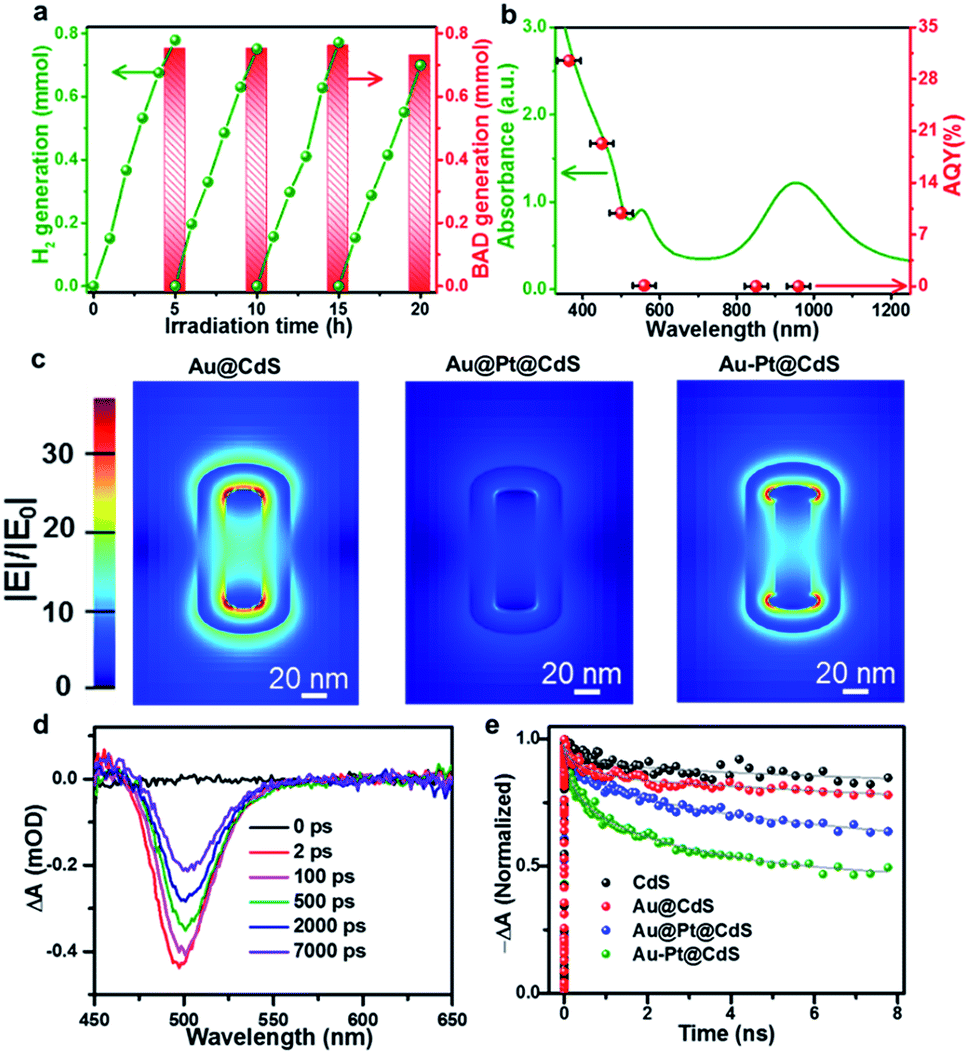 | ||
| Fig. 3 (a) Long-term photocatalytic conversion of BA using Au–Pt@CdS under Vis-NIR light (λ > 420 nm) irradiation. (b) Absorption spectra of Au–Pt@CdS and apparent quantum yield efficiency (AQY) of hydrogen evolution from BA under different monochromatic lights. Error bars refer to the wavelength range of the incident light. (c) Local electric field distributions of metal–CdS hybrids at L-SPR excitation calculated by the finite-difference time-domain method. (d) Transient absorption (TA) spectra of Au–Pt@CdS with time delays after 370 nm excitation. (e) Comparison of the exciton bleach recovery kinetics for CdS and metal–CdS hybrids probed at 503 nm and their corresponding fits. | ||
Since electric field distribution and intensity are related to the SPR enhancement,25,45,46 we simulated the electric field (|E|/|E0|) distribution around different metal–CdS hybrids, aiming to ascertain the region of electric field enhancement upon SPR excitation and its possible contribution to the photoactivity enhancement. As shown in Fig. 3c, differing from strong electric field distribution at both ends of binary Au@CdS, the ternary Au@Pt@CdS sample exhibits weak electric field enhancement. When the continuous Pt shell encapping the entire surface of Au NRs in Au@Pt@CdS is replaced by discrete Pt selectively tipped onto the two ends of Au NRs in Au–Pt@CdS, the electric field enhancement around the surface of Au–Pt@CdS is greatly boosted. The weakest electric field enhancement of Au@Pt@CdS could be ascribed to the plasmon-induced electron transfer from Au to Pt and the serious plasmon damping effect of the continuous Pt shell.23–25,36 According to the simulation result, the maximum values of electric field enhancement at the outside surface of CdS for Au@CdS, Au–Pt@CdS and Au@Pt@CdS are about 15, 13 and 5, respectively. The enhanced electric field can improve the light harvesting ability of the catalyst, and increase the generation and separation rate of electron–hole pairs near the surface of the semiconductor material.45–47 However, the trend in electric field enhancement (i.e., Au@CdS > Au–Pt@CdS ≫ Au@Pt@CdS) is inconsistent with that of photoactivity (i.e., Au–Pt@CdS > Au@Pt@CdS > Au@CdS). This indicates that in addition to the effect of electric field enhancement factor on the photoactivity of metal–semiconductor hybrids, other factors should be simultaneously considered to account for the difference in photoactivity enhancement.
We then investigated charge transfer dynamics in CdS and metal–CdS hybrids by using ultrafast transient absorption (TA) spectroscopy. Upon 370 nm excitation, a negative absorption peak at about 500 nm corresponding to the ground state bleach (GSB) signal of the CdS component is formed due to the band-filling by photoinduced electrons and holes (Fig. 3d and S10†). The recovery kinetics of this GSB reflects the charge dissipating processes by recombination and/or transfer (Fig. 3e). In blank CdS, the recovery kinetics originates from the recombination of charge carriers and the possible charge trapping by the defects.15,48 In the presence of metal nanostructures, the kinetics become significantly faster. We attribute this observation to the photoinduced electron transfer from CdS to the metal ingredient, as reported in similar semiconductor–metal composites.11,29,49 In order to quantitatively determine the electron transfer rate, the recovery kinetics were fitted by a biexponential function and the electron transfer rates were estimated by comparing the charge transfer rate constants (kct, see eqn (S1)–(S3) and Table S2†).50 In comparison with blank CdS, the charge transfer rate over binary Au@CdS is increased, which indicates an electron transfer channel from CdS to Au because the work function of Au (5.10 eV) is larger than that of CdS (4.20 eV).51,52 After the Pt NPs (with a work function of 5.40 eV) are deposited on Au NRs, the kct values of both Au@Pt@CdS and Au–Pt@CdS are further enhanced. The highest kct value for Au–Pt@CdS signifies that the Au–Pt bimetal nanostructure is more effective than Au@Pt in facilitating the photoexcited charge transfer in the photocatalytic system, due to the additional interfacial electron transfer channels from CdS to Au and to Pt guaranteed by the direct contact and matched band alignment among the three components (Fig. S11†).51,52
To study the effect of SPR excitation on photoactivity enhancement, we performed a wavelength-control experiment over Au–Pt@CdS under selective photoexcitation of the plasmonic Au–Pt component (Fig. S12a†).31,53 It is seen from Fig. S12b† that the Au–Pt@CdS hybrids show only trace photoactivity under SPR excitation alone, indicating that the effect of hot electron injection from Au–Pt to CdS on the photoactivity is negligible. When we used the photon energy at 570 nm to excite the T-SPR of Au–Pt@CdS in the TA measurement, the sample shows no signal corresponding to excitation and relaxation kinetics (Fig. S12c†), which further confirms the absence of the hot electron transfer process. Thus, the SPR enhancement mechanisms should be interpreted in terms of the electric field effect.45 In addition, wavelength-control experiments under selective photoexcitation of CdS or simultaneous photoexcitation of CdS and Au–Pt (Fig. S13a†) disclose that the Au–Pt@CdS exhibits enhanced photoactivity as compared to bare CdS under both irradiation conditions, and the photoactivity enhancement is more prominent under simultaneous photoexcitation of CdS and Au–Pt components (Fig. S13b†). We also prepared nonplasmonic Pt-loaded CdS (Pt–CdS) through the well-reported photodeposition method.44,54 The photocatalytic activity of nonplasmonic Pt–CdS is much lower than that of plasmonic Au–Pt@CdS under Vis-NIR light irradiation (Fig. S13c†).
The above joint results signify that the promoted photoactivity of Au–Pt@CdS is induced by the synergistic coupling of the band-gap photoexcitation of semiconductor CdS with the electric field enhancement and the electron sink effect of Au–Pt bimetal, as depicted in Fig. 4a.55,56 Specifically, when the Au–Pt@CdS ternary heterostructure is illuminated by Vis-NIR light (λ > 420 nm), the CdS component can harvest short-wavelength visible light (420 nm < λ < 520 nm), yielding electron–hole charge carriers (e−–h+). Meanwhile, the SPR excitation of plasmonic Au–Pt bimetal by longer-wavelength light irradiation provides extra electric field enhancement to improve the photoabsorption, and promote the generation and separation of electron–hole pairs in CdS.45,46,57 Subsequently, the photogenerated electrons traverse from the conduction band (CB) of CdS to the anisotropic Au–Pt bimetal component. The protons (H+) diffuse through the loose and porous CdS thin layer and react with electrons to generate H2.35,58,59 The holes retained in the valence band (VB) of CdS can selectively oxidize alcohols to aldehydes, which is the overall activity-limiting step in the redox cycle.44,60 The photogenerated electrons and holes are spatially separated, significantly reducing the recombination probability, which leads to greatly improved photoactivity of Au–Pt@CdS.
 | ||
| Fig. 4 (a) Schematic illustration of the energy band alignment and SPR-coupled multichannel electron transfer in Au–Pt@CdS heterostructures. (b) Photocurrent density versus time (I–t) curves, (c) electrochemical impedance spectroscopy (EIS) Nyquist plots and (d) Mott–Schottky plots of CdS and metal–CdS hybrids under Vis-NIR light (λ > 420 nm) irradiation. (e) Linear sweep voltammetry (LSV) curves of CdS and metal–CdS electrodes. | ||
The investigation of the photoelectrochemical (PEC) process can further reveal the picture of electron transfer and the underlying photoactivity enhancement mechanism. As shown in Fig. 4b, transient photocurrent responses of different samples under chopped Vis-NIR light illumination indicate that the construction of bimetal–semiconductor hybrids is conducive to enhancing the photocurrent of semiconductor CdS, which follows the same order as the photoactivity: Au–Pt@CdS > Au@Pt@CdS > Au@CdS > CdS. This result indicates a more effective separation of electron–hole pairs over Au–Pt@CdS than other electrode samples.9,35,61,62 Au–Pt@CdS and Au@Pt@CdS consist of the same hetero-components, but the anisotropic Au–Pt@CdS exhibits higher photocurrent and photoactivity than isotropic Au@Pt@CdS under Vis-NIR light illumination. This suggests that the inappropriate arrangement of the plasmonic–nonplasmonic bimetal heterostructure in Au@Pt@CdS leads to the suppression of electric field enhancement and electron sink effect, as respectively proved by the results of electric field simulation (Fig. 3c) and TA characterization (Fig. 3e).24,25
Electrochemical impedance spectroscopy (EIS, Fig. 4c) and Mott–Schottky (Fig. 4d) analysis were conducted under Vis-NIR light illumination. The arc at the middle frequencies of the Nyquist plot in Fig. 4c is characteristic of charge transportation resistance.63 Apparently, the diameter of the arc for the Au–Pt@CdS electrode is much smaller than that of CdS, Au@CdS and Au@Pt@CdS, indicating that the resistance of interfacial charge transportation is significantly decreased over the Au–Pt@CdS electrode. The Mott–Schottky analysis can be used to provide fundamental insights into the charge carrier density (ND), which is obtained from the following equation:63,64
Conclusions
In summary, we have accomplished a controllable design of bimetal–semiconductor hybrids for optimizing the redox photocatalysis performance of alcohol conversion to H2 and value-added aldehyde for the first time. Experimental results and theoretical analyses indicate that the composition and spatial configurations of metal components have significant influences on photoabsorption, local electric field distribution and photoinduced charge carrier transfer rate in bimetal–semiconductor heterostructures. Compared with blank CdS and other metal–CdS composites, Au–Pt@CdS exhibits collective advantages for photoredox catalysis as follows. (1) The unique SPR of Au NRs improves light absorption and induces local electric field enhancement, which can promote the charge carrier generation/migration of CdS. (2) Pt NPs anisotropically located at the tips of Au NRs serve as an electron reservoir and a co-catalyst to steer the directional charge flow and facilitate the proton reduction. (3) The intimate and multiple metal–metal and metal–semiconductor heterointerfaces ensure the spatially regulated multichannel electron transfer and maximized plasmon–exciton interactions. Mechanistic studies demonstrated that the photoactivity of Au–Pt@CdS is driven by the photogenerated charge carriers from semiconductor CdS instead of the plasmonic Au–Pt bimetal. It is hoped that this facile strategy for controllable synthesis of bimetal–semiconductor hybrids, as well as the underlying SPR-coupled multichannel electron transfer mechanism illustrated here, could be instructive for further rational design of plasmonic bimetal– or multimetal–semiconductor hybrids toward efficient redox catalysis.Experimental section
Chemicals and materials
All chemicals were analytical grade and used without further purification. Hexadecyltrimethylammonium bromide (C19H42NBr, CTAB), silver nitrate (AgNO3), sodium borohydride (NaBH4), L-ascorbic acid (C6H8O6, AA), hydrochloric acid (HCl, 37 wt%) and benzotrifluoride (C7H5F3, BTF) were purchased from Sigma Aldrich. Benzyl alcohol (C7H8O, BA), benzaldehyde (C7H6O, BAD) and sodium oleate (C18H33O2Na, NaOL) were purchased from Aladdin. 4-Methylbenzyl alcohol (C8H10O), 4-methoxybenzyl alcohol (C8H10O2), 4-chlorobenzyl alcohol (C7H7ClO), and 4-hydroxybenzyl alcohol (C7H8O2) were supplied by Alfa Aesar. Cadmium acetate (C4H6O4Cd, Cd(Ac)2), thioacetamide (C2H5SN, TAA), chloroauric acid tetrahydrate (HAuCl4·4H2O), glycine acid (C2H5NO2, Gly), anhydrous ethanol (C2H5OH, EtOH) and chloroplatinic acid hexahydrate (H2PtCl6·6H2O) were obtained from Sinopharm Chemical Reagent Co., Ltd (Shanghai, China). Deionized water used in the synthesis was obtained from local sources.Synthesis of Au NRs
The Au NRs were prepared using a seed-mediated growth method.68 The seed solution for Au NR growth was prepared as follows: 5 mL of 0.5 mM HAuCl4 was mixed with 5 mL of 0.2 M CTAB solution in a 20 mL scintillation vial. 0.6 mL of fresh 0.01 M NaBH4 was diluted to 1 mL with water and was then injected into the above solution under vigorous stirring (1200 rpm). The solution color changed from yellow to brownish yellow and the stirring was stopped after 2 min. The seed solution was aged at room temperature for 2 h before use. Subsequently, 1.4 g of CTAB and 0.25 g of NaOL were dissolved in 50 mL of warm water (∼50 °C) in a 100 mL Erlenmeyer flask. The solution was allowed to cool down to 30 °C and 3.6 mL of 4 mM AgNO3 solution was added. The mixture was kept undisturbed at 30 °C for 15 min after which 50 mL of 1 mM HAuCl4 solution was added. The solution became colorless after 90 min of stirring (700 rpm) and 0.3 mL of HCl (37 wt% in water, 12.1 M) was then introduced. After another 15 min of slow stirring at 400 rpm, 0.25 mL of 0.064 M AA was added and the solution was vigorously stirred for 30 s. Finally, 0.4 mL of seed solution was injected into the growth solution. The resultant mixture was stirred for 30 s and left undisturbed at 30 °C for 12 h for NR growth.Preparation of Au–Pt
Au–Pt was prepared by using Au NRs as the template.24 Briefly, 10 mL of the prepared Au NRs was separated from excess CTAB by centrifugation twice (at 10![[thin space (1/6-em)]](https://www.rsc.org/images/entities/char_2009.gif) 000 rpm) and redispersed in 0.1 M CTAB solution. Then, 0.568 mL of 0.1 M ascorbic acid was added into 10 mL of as-made Au NR suspension. 100 μL of 0.01 M H2PtCl6·6H2O and subsequently 0.08 mL of 0.01 M HCl were added to the reaction mixture. The mixture was left undisturbed for 24 h at 30 °C. Pt-covered Au NRs (Au@Pt) were prepared by using Au NRs in 0.03 M CTAB solution as the template following the same procedure.
000 rpm) and redispersed in 0.1 M CTAB solution. Then, 0.568 mL of 0.1 M ascorbic acid was added into 10 mL of as-made Au NR suspension. 100 μL of 0.01 M H2PtCl6·6H2O and subsequently 0.08 mL of 0.01 M HCl were added to the reaction mixture. The mixture was left undisturbed for 24 h at 30 °C. Pt-covered Au NRs (Au@Pt) were prepared by using Au NRs in 0.03 M CTAB solution as the template following the same procedure.
Preparation of Au–Pt@CdS
For the synthesis of Au–Pt@CdS, 10 mL of the as-prepared Au–Pt seeds and 10 mL of aqueous Gly solution (0.2 M) were mixed in a 50 mL vial, and subsequently 300 μL aqueous NaOH solution (2 M) was added to the reaction mixture. The mixture was kept at 30 °C for 30 min without stirring. Next, 200 μL of Cd(Ac)2 (0.1 M) and TAA (0.1 M) solution were injected into the above solution drop by drop. The reaction was allowed to proceed at 85 °C under vigorous stirring for 2 h. The suspensions were centrifuged at 12000 rpm for 10 min and washed with ethanol three times, and then the precipitates were vacuum dried at 40 °C. Au@CdS, Au@Pt@CdS and blank CdS were also synthesized by the above method, except that the corresponding seeds or blank CTAB (0.1 M) aqueous solution was used instead of Au–Pt, respectively, in the synthesis process. The Au–Pt/CdS sample was prepared by mixing the blank CdS with an appropriate amount of Au–Pt in solution with vigorous stirring for 24 h followed by the wash and dry process similar to Au–Pt@CdS.
Material characterization
The crystal phase properties of the samples were analysed with a Bruker D8 Advance X-ray diffractometer (XRD) using Ni-filtered Cu Kα radiation at 40 kV and 40 mA in the 2θ range from 20° to 80° with a scan rate of 0.02° per second. The optical properties of the samples were characterized using a Cary-5000 ultraviolet-visible-near infrared diffuse reflectance spectrophotometer (DRS, Varian Co.). The morphology and elemental distribution of the samples were analysed by field-emission scanning electron microscopy (FESEM) on a FEI Nova NANOSEM 230 spectrophotometer and transmission electron microscopy (TEM), high-resolution TEM (HRTEM) and elemental mapping analysis using a JEOL 2100F instrument at an accelerating voltage of 200 kV. Raman spectroscopy was performed on a Renishaw inVia Raman System 1000 with a 532 nm Nd:YAG excitation source at room temperature. X-ray photoelectron spectroscopy (XPS) measurements were performed using a Thermo Scientific ESCA Lab250 spectrometer that consists of monochromatic Al Kα as the X-ray source, a hemispherical analyser, and a sample stage with multiaxial adjustability to obtain the composition on the surface of the samples. All of the binding energies were calibrated using the C 1s peak of the surface adventitious carbon at 284.6 eV. The elemental concentration analysis was performed using an inductively coupled plasma emission spectroscopy instrument (ICP, PerkinElmer Optima 8000). The carrier dynamics were measured by using femtosecond transient absorption spectroscopy (Time-Tech Spectra, femtoTA-100). Part of the 800 nm output pulse from the amplifier was used to pump a TOPAS Optical Parametric Amplifier (OPA) which generates the 370 nm pump beam. The pump pulses were chopped by a synchronized chopper at 500 Hz and the absorbance change was calculated with two adjacent probe pulses (pump-blocked and pump-unblocked), and the pump power was approximately 1 μW. The samples were dispersed in water for all pump–probe characterizations performed under ambient conditions. The photoelectrochemical analysis was carried out in a conventional three-electrode cell using a Pt plate and an Ag/AgCl electrode as the counter electrode and reference electrode, respectively. The electrolyte was 0.2 M Na2SO4 aqueous solution containing 0.1 mM BA. The working electrode was prepared on indium-tin oxide (ITO) glass that was cleaned by sonication in ethanol for 30 min and dried at 353 K. The boundary of ITO glass was protected using Scotch tape. 5 mg of the sample was dispersed in 0.5 mL of N,N-dimethylformamide (DMF, supplied by Sinopharm Chemical Reagent Co., Ltd) by sonication to get a slurry. The slurry (20 μL) was spread onto pre-treated ITO glass. After air drying, the working electrode was further dried at 393 K for 2 h to improve adhesion. Then, the Scotch tape was unstuck, and the uncoated part of the electrode was isolated with epoxy resin. The exposed area of the working electrode was 0.25 cm2. The light irradiation source was a 300 W Xe arc lamp system equipped with a filter to cut off light of wavelength λ < 420 nm. The cathodic polarization curves were obtained using the linear sweep voltammetry (LSV) technique with a scan rate of 2 mV s−1. The electrochemical impedance spectroscopy (EIS) experiments were conducted on an AUTOLAB M204 workstation.FDTD simulations
The electric field simulations were carried out by using a finite-difference time-domain (FDTD) software package (Lumerical Solutions, Inc.). The refractive indices of CdS, BTF, Au and Pt were taken from previous reported data.19,23,69 A total-field/scattered field (TFSF) source was used as an incident field into the simulation region, which coincided with the wavelength of our experimental irradiation source. Perfectly matched layer (PML) boundary conditions were used in our simulations. The Au NRs are cylinders with round ends and the size was taken to match their average values. The radius of the cylinder is 14.5 nm and radii of the ends are 8 nm. The total length of the Au NRs is 92.5 nm. The shell thickness of CdS is 20 nm. For the model of Au–Pt@CdS, elliptical Pt spheres with diameters of 14 nm were located at both ends of the Au NRs with a total length of 98 nm. For Au@Pt@CdS, the Pt shell is a cylinder with a radius of 2.1 nm and the total length of the Au NRs is 107.9 nm.Photoactivity
The experiments were performed referring to the previously reported literature with some modifications.44,70 In a typical photocatalytic reaction, 2 mL catalyst suspension (1 mg mL−1 in BTF) containing 0.5 M alcohol was placed in a quartz reactor (25 mL) equipped with a magnetic stir bar. The reaction suspension was sonicated for 2 min at room temperature and purged with Ar gas for 30 min. The reactor was then tightly sealed and then stirred for 30 minutes in the dark to achieve an adsorption–desorption equilibrium. A 300 W Xe arc lamp (PLS-SXE 300, Beijing Perfect light Co., Ltd) with a filter to cut off light of wavelength λ < 420 nm was used as the irradiation source. The light intensity was fixed at 800 mW cm−2. The photon flux of incident light was measured using an Optical Power/Energy Meter (Newport 842-PE). The irradiation area is 3.8 cm2. During photocatalysis, the suspension was continuously stirred to ensure uniform irradiation. The evolved gases were analysed using a gas chromatograph (Shimadzu GC-2014C, MS-5 A column, Ar carrier) equipped with a thermal conductivity detector (TCD). Products in solution were quantified using an Agilent Gas Chromatograph (GC-7820) with a flame-ionization detector (FID) and identified by gas chromatography-mass spectrometry (GC-MS, Agilent Technologies, GC6890N, MS 5973). The recycling test for photocatalytic conversion of BA over Au–Pt@CdS was performed as follows. After 5 h reaction under Vis-NIR light irradiation, the suspension was centrifuged and mixed with 2 mL BTF containing 0.5 M BA for continuous test. The conversion of BA and selectivity for BAD were calculated with the following equations:71
here C0 is the initial concentration of BA; CBA and CBAD are the concentrations of the residual BA and the corresponding BAD at a certain time after the catalytic reaction, respectively. The apparent quantum efficiency (AQE) was calculated from the ratio of twice the number of H2 molecules to the number of incident photons by using the following expression:22,31

where M is the molar amount of H2 molecules, NA is the Avogadro constant, h is the Planck constant, c is the speed of light, S is the irradiation area, P is the intensity of the irradiation, t is the photoreaction time and λ is the wavelength of the monochromatic light. The power density of different monochromatic lights was fixed at 30.0 mW cm−2.
Conflicts of interest
There are no conflicts to declare.Acknowledgements
The support from the National Natural Science Foundation of China (NSFC) (21872029, U1463204, 21173045), the Award Program for Minjiang Scholar Professorship, the Natural Science Foundation (NSF) of Fujian Province for Distinguished Young Investigator Rolling Grant (2017J07002), the Independent Research Project of the State Key Laboratory of Photocatalysis on Energy and Environment (No. 2014A05), and the 1st Program of Fujian Province for Top Creative Young Talents is gratefully acknowledged.Notes and references
- J. C. Colmenares and R. Luque, Chem. Soc. Rev., 2014, 43, 765–778 RSC
.
- M.-Q. Yang, N. Zhang, M. Pagliaro and Y.-J. Xu, Chem. Soc. Rev., 2014, 43, 8240–8254 RSC
- G. Xie, K. Zhang, B. Guo, Q. Liu, L. Fang and J. R. Gong, Adv. Mater., 2013, 25, 3820–3839 CrossRef CAS PubMed
- N. Zhang, C. Han, Y.-J. Xu, J. J. Foley IV, D. Zhang, J. Codrington, S. K. Gray and Y. Sun, Nat. Photonics, 2016, 10, 473–482 CrossRef CAS
- Z. Yin, J. Guo, S. Lin, Y. Zhu, H. Ke, Y. Zheng and Z. Tang, Sci. Adv., 2017, 3, e1701162 CrossRef PubMed
- W. Jiang, S. Bai, L. Wang, X. Wang, L. Yang, Y. Li, D. Liu, X. Wang, Z. Li, J. Jiang and Y. Xiong, Small, 2016, 12, 1640–1648 CrossRef CAS PubMed
- K.-Q. Lu, X. Xin, N. Zhang, Z.-R. Tang and Y.-J. Xu, J. Mater. Chem. A, 2018, 6, 4590–4604 RSC
- J. Chen, X.-J. Wu, L. Yin, B. Li, X. Hong, Z. Fan, B. Chen, C. Xue and H. Zhang, Angew. Chem., Int. Ed., 2015, 54, 1210–1214 CrossRef CAS PubMed
- C. Han, S.-H. Li, Z.-R. Tang and Y.-J. Xu, Chem. Sci., 2018, 9, 8914–8922 RSC
- B. Weng, K.-Q. Lu, Z. Tang, H. M. Chen and Y.-J. Xu, Nat. Commun., 2018, 9, 1543 CrossRef PubMed
- W.-T. Chen, T.-T. Yang and Y.-J. Hsu, Chem. Mater., 2008, 20, 7204–7206 CrossRef CAS
- S. Han, L. Hu, N. Gao, A. A. Al-Ghamdi and X. Fang, Adv. Funct. Mater., 2014, 24, 3725–3733 CrossRef CAS
- J. D. Xiao, L. Han, J. Luo, S. H. Yu and H. L. Jiang, Angew. Chem., Int. Ed., 2018, 57, 1103–1107 CrossRef CAS PubMed
- X. Liu, J. Iocozzia, Y. Wang, X. Cui, Y. Chen, S. Zhao, Z. Li and Z. Lin, Energy Environ. Sci., 2017, 10, 402–434 RSC
- H.-Q. Xu, S. Yang, X. Ma, J. Huang and H.-L. Jiang, ACS Catal., 2018, 8, 11615–11621 CrossRef CAS
- N. Zhang, C. Han, X. Fu and Y.-J. Xu, Chem, 2018, 4, 1832–1861 CAS
- L. Zhang, Z. Xie and J. Gong, Chem. Soc. Rev., 2016, 45, 3916–3934 RSC
- H. Huang, L. Zhang, Z. Lv, R. Long, C. Zhang, Y. Lin, K. Wei, C. Wang, L. Chen, Z.-Y. Li, Q. Zhang, Y. Luo and Y. Xiong, J. Am. Chem. Soc., 2016, 138, 6822–6828 CrossRef CAS PubMed
- Z. Zheng, T. Tachikawa and T. Majima, J. Am. Chem. Soc., 2014, 137, 948–957 CrossRef PubMed
- Y. Yin, Y. Yang, L. Zhang, Y. Li, Z. Li, W. Lei, Y. Ma and Z. Huang, RSC Adv., 2017, 7, 36923–36928 RSC
- S.-F. Hung, Y.-C. Yu, N.-T. Suen, G.-Q. Tzeng, C.-W. Tung, Y.-Y. Hsu, C.-S. Hsu, C.-K. Chang, T.-S. Chan, H.-S. Sheu, J.-F. Lee and H. M. Chen, Chem. Commun., 2016, 52, 1567–1570 RSC
- Q. Li, B. Guo, J. Yu, J. Ran, B. Zhang, H. Yan and J. R. Gong, J. Am. Chem. Soc., 2011, 133, 10878–10884 CrossRef CAS PubMed
- M. Grzelczak, J. Pérez-Juste, F. J. García de Abajo and L. M. Liz-Marzán, J. Phys. Chem. C, 2007, 111, 6183–6188 CrossRef CAS
- Z. Zheng, T. Tachikawa and T. Majima, J. Am. Chem. Soc., 2014, 136, 6870–6873 CrossRef CAS PubMed
- J. Guo, Y. Zhang, L. Shi, Y. Zhu, M. F. Mideksa, K. Hou, W. Zhao, D. Wang, M. Zhao, X. Zhang, J. Lv, J. Zhang, X. Wang and Z. Tang, J. Am. Chem. Soc., 2017, 139, 17964–17972 CrossRef CAS PubMed
- S. Bai, X. Li, Q. Kong, R. Long, C. Wang, J. Jiang and Y. Xiong, Adv. Mater., 2015, 27, 3444–3452 CrossRef CAS PubMed
- S.-C. Lin, C.-S. Hsu, S.-Y. Chiu, T.-Y. Liao and H. M. Chen, J. Am. Chem. Soc., 2017, 139, 2224–2233 CrossRef CAS PubMed
- R. Long, Y. Li, L. Song and Y. J. Xiong, Small, 2015, 11, 3873–3889 CrossRef CAS PubMed
- J. Wu, Z. Zhang, B. Liu, Y. Fang, L. Wang and B. Dong, Sol. RRL, 2018, 2, 1800039 CrossRef
- J. Zhu, Y. Yang, L. Chen, W. Xiao, H. Liu, H. D. Abruña and D. Wang, Chem. Mater., 2018, 30, 5987–5995 CrossRef CAS
- C. Han, Q. Quan, H. M. Chen, Y. Sun and Y.-J. Xu, Small, 2017, 13, 1602947 CrossRef PubMed
- X.-J. Wu, J. Chen, C. Tan, Y. Zhu, Y. Han and H. Zhang, Nat. Chem., 2016, 8, 470 CrossRef CAS PubMed
- A. Li, P. Zhang, X. Chang, W. Cai, T. Wang and J. Gong, Small, 2015, 11, 1892–1899 CrossRef CAS PubMed
- A. Li, X. Chang, Z. Huang, C. Li, Y. Wei, L. Zhang, T. Wang and J. Gong, Angew. Chem., Int. Ed., 2016, 55, 13734–13738 CrossRef CAS PubMed
- X. Ma, K. Zhao, H. Tang, Y. Chen, C. Lu, W. Liu, Y. Gao, H. Zhao and Z. Tang, Small, 2014, 10, 4664–4670 CrossRef CAS PubMed
- L. Ma, K. Chen, F. Nan, J.-H. Wang, D.-J. Yang, L. Zhou and Q.-Q. Wang, Adv. Funct. Mater., 2016, 26, 6076–6083 CrossRef CAS
- C. Han, Z. Chen, N. Zhang, J. C. Colmenares and Y.-J. Xu, Adv. Funct. Mater., 2015, 25, 221–229 CrossRef CAS
- Y. Hu, X. Gao, L. Yu, Y. Wang, J. Ning, S. Xu and X. W. Lou, Angew. Chem., Int. Ed., 2013, 52, 5636–5639 CrossRef CAS PubMed
- J. Zhang, Y. Tang, K. Lee and M. Ouyang, Science, 2010, 327, 1634–1638 CrossRef CAS PubMed
- H. Wang, Z. Sun, Q. Lu, F. Zeng and D. Su, Small, 2012, 8, 1167–1172 CrossRef CAS PubMed
- H. Ataee-Esfahani, L. Wang, Y. Nemoto and Y. Yamauchi, Chem. Mater., 2010, 22, 6310–6318 CrossRef CAS
- J. S. Suh and J. S. Lee, Chem. Phys. Lett., 1997, 281, 384–388 CrossRef CAS
- M. Li, X.-F. Yu, S. Liang, X.-N. Peng, Z.-J. Yang, Y.-L. Wang and Q.-Q. Wang, Adv. Funct. Mater., 2011, 21, 1788–1794 CrossRef CAS
- Z. Chai, T.-T. Zeng, Q. Li, L.-Q. Lu, W.-J. Xiao and D. Xu, J. Am. Chem. Soc., 2016, 138, 10128–10131 CrossRef CAS PubMed
- J. Xu, W.-M. Yang, S.-J. Huang, H. Yin, H. Zhang, P. Radjenovic, Z.-L. Yang, Z.-Q. Tian and J.-F. Li, Nano Energy, 2018, 49, 363–371 CrossRef CAS
- J.-J. Chen, J. C. S. Wu, P. C. Wu and D. P. Tsai, J. Phys. Chem. C, 2012, 116, 26535–26542 CrossRef CAS
- H. Gao, P. Zhang, J. Zhao, Y. Zhang, J. Hu and G. Shao, Appl. Catal., B, 2017, 210, 297–305 CrossRef CAS
- M.-Q. Yang, Y.-J. Xu, W. Lu, K. Zeng, H. Zhu, Q.-H. Xu and G. W. Ho, Nat. Commun., 2017, 8, 14224 CrossRef CAS PubMed
- Y. Du, B. Chen, Z. Yin, Z. Liu and H. Zhang, Small, 2014, 10, 4727–4734 CrossRef CAS PubMed
- Z. Zhang, Y. Huang, K. Liu, L. Guo, Q. Yuan and B. Dong, Adv. Mater., 2015, 27, 5906–5914 CrossRef CAS PubMed
- X. Wang, C. Liow, A. Bisht, X. Liu, T. C. Sum, X. Chen and S. Li, Adv. Mater., 2015, 27, 2207–2214 CrossRef CAS PubMed
- A. Tanaka, K. Nakanishi, R. Hamada, K. Hashimoto and H. Kominami, ACS Catal., 2013, 3, 1886–1891 CrossRef CAS
- Y.-C. Pu, G. Wang, K.-D. Chang, Y. Ling, Y.-K. Lin, B. C. Fitzmorris, C.-M. Liu, X. Lu, Y. Tong and J. Z. Zhang, Nano Lett., 2013, 13, 3817–3823 CrossRef CAS PubMed
- A. Tanaka, K. Hashimoto and H. Kominami, J. Am. Chem. Soc., 2014, 136, 586–589 CrossRef CAS PubMed
- Z. Zhang, A. Li, S.-W. Cao, M. Bosman, S. Li and C. Xue, Nanoscale, 2014, 6, 5217–5222 RSC
- Y.-H. Chiu, K.-D. Chang and Y.-J. Hsu, J. Mater. Chem. A, 2018, 6, 4286–4296 RSC
- C. Li, P. Wang, Y. Tian, X. Xu, H. Hou, M. Wang, G. Qi and Y. Jin, ACS Catal., 2017, 7, 5391–5398 CrossRef CAS
- L. Ma, S. Liang, X.-L. Liu, D.-J. Yang, L. Zhou and Q.-Q. Wang, Adv. Funct. Mater., 2015, 25, 898–904 CrossRef CAS
- D. Seo, G. Park and H. Song, J. Am. Chem. Soc., 2012, 134, 1221–1227 CrossRef CAS PubMed
- S. Meng, X. Ye, J. Zhang, X. Fu and S. Chen, J. Catal., 2018, 367, 159–170 CrossRef CAS
- B. Weng, Q. Quan and Y.-J. Xu, J. Mater. Chem. A, 2016, 4, 18366–18377 RSC
- M. Wang, X. Pang, D. Zheng, Y. He, L. Sun, C. Lin and Z. Lin, J. Mater. Chem. A, 2016, 4, 7190–7199 RSC
- Z. Xu, Y. Lin, M. Yin, H. Zhang, C. Cheng, L. Lu, X. Xue, H. J. Fan, X. Chen and D. Li, Adv. Mater. Interfaces, 2015, 2, 1500169 CrossRef
- F.-X. Xiao, J. Miao, H.-Y. Wang, H. Yang, J. Chen and B. Liu, Nanoscale, 2014, 6, 6727–6737 RSC
- G. A. Samara, Phys. Rev. B: Condens. Matter Mater. Phys., 1983, 27, 3494–3505 CrossRef CAS
- N. Zhang, Y. Zhang, X. Pan, M.-Q. Yang and Y.-J. Xu, J. Phys. Chem. C, 2012, 116, 18023–18031 CrossRef CAS
- S. Bai, J. Jiang, Q. Zhang and Y. Xiong, Chem. Soc. Rev., 2015, 44, 2893–2939 RSC
- X. Ye, Y. Gao, J. Chen, D. C. Reifsnyder, C. Zheng and C. B. Murray, Nano Lett., 2013, 13, 2163–2171 CrossRef CAS PubMed
- M. S. Gomez, J. M. Guerra and F. Vilches, Appl. Opt., 1985, 24, 1147–1150 CrossRef CAS
- D. Jiang, X. Chen, Z. Zhang, L. Zhang, Y. Wang, Z. Sun, R. M. Irfan and P. Du, J. Catal., 2018, 357, 147–153 CrossRef
- N. Zhang, M.-Q. Yang, Z.-R. Tang and Y.-J. Xu, ACS Nano, 2014, 8, 623–633 CrossRef CAS PubMed
Footnote |
| † Electronic supplementary information (ESI) available: Additional characterizations and discussions, 13 figures and 3 tables. See DOI: 10.1039/c8sc05813j |
| This journal is © The Royal Society of Chemistry 2019 |