
 Open Access Article
 This Open Access Article is licensed under a Creative Commons Attribution-Non Commercial 3.0 Unported Licence
Synthetic 2-D lead tin sulfide nanosheets with tuneable optoelectronic properties from a potentially scalable reaction pathway†
Kane
Norton‡
a,
Jens
Kunstmann‡
 *b,
Lu
Ping
a,
Alexander
Rakowski
c,
Chuchen
Wang
a,
Alexander J.
Marsden
ad,
Ghulam
Murtaza
c,
Niting
Zeng
a,
Simon J.
McAdams
ac,
Mark A.
Bissett
ad,
Sarah J.
Haigh
ad,
Brian
Derby
a,
Gotthard
Seifert
b and
David J.
Lewis
*a
*b,
Lu
Ping
a,
Alexander
Rakowski
c,
Chuchen
Wang
a,
Alexander J.
Marsden
ad,
Ghulam
Murtaza
c,
Niting
Zeng
a,
Simon J.
McAdams
ac,
Mark A.
Bissett
ad,
Sarah J.
Haigh
ad,
Brian
Derby
a,
Gotthard
Seifert
b and
David J.
Lewis
*a
aSchool of Materials University of Manchester, Oxford Road, Manchester, UK M13 9PL. E-mail: david.lewis-4@manchester.ac.uk
bTheoretische Chemie, Technische Universität Dresden, 01069 Dresden, Germany. E-mail: jens.kunstmann@tu-dresden.de
cSchool of Chemistry, University of Manchester, Oxford Road, Manchester, UK M13 9PL
dNational Graphene Institute, University of Manchester, Oxford Road, Manchester, UK M13 9PL
First published on 31st October 2018
Abstract
Solventless thermolysis of molecular precursors followed by liquid phase exfoliation allows access to two-dimensional IV–VI semiconductor nanomaterials hitherto unreachable by a scalable processing pathway. Firstly, the use of metal dithiocarbamate precursors to produce bulk alloys in the series Pb1−xSnxS (0 ≤ x ≤ 1) by thermolysis is demonstrated. The bulk powders are characterised by powder X-ray diffraction (pXRD), Raman spectroscopy, scanning electron microscopy (SEM) and energy dispersive X-ray (EDX) spectroscopy. It was found that there is a transition from cubic structures for the Pb-rich alloys including the end compound, PbS (0 ≤ x ≤ 0.4) to layered orthorhombic structures for Sn-rich alloys and the end compound SnS (0.5 ≤ x ≤ 1.0). A smooth elemental progression from lead-rich to tin-rich monochalcogenides across the series of materials is observed. Liquid phase exfoliation was applied to produce two dimensional (2D) nanosheets for a mixed Pb1−xSnxS alloy (where x = 0.8) in 1-methyl-2-pyrrolidone (NMP) using the synthetic bulk powder as starting material. The nanosheet products were characterized by SEM, atomic force microscopy (AFM) and high angle annular dark field scanning transmission electron microscopy (HAADF STEM). First principle calculations of Pb1−xSnxS alloys show that the Sn content x modifies the size of the band gap by several 100 meV and that x changes the gap type from indirect in SnS to direct in Pb0.2Sn0.8S. These results are supported by UV-Vis spectroscopy of exfoliated Pb0.2Sn0.8S. The method employed demonstrates a new, scalable, processing pathway which can potentially be used to synthesize a range of synthetic layered structures that can be exfoliated to as-yet unaccessed 2D materials with tunable electronic properties.
Introduction
Significant academic effort has been directed towards to the synthesis of graphene1 and other 2-dimensional (2D) materials,2 which have attracted considerable interest due to emergent properties in the monolayer form. Layered transition metal chalcogenides3 (TMCs) such as molybdenum disulfide (MoS2) and tungsten disulfide (WS2) have also been of interest, as they are intrinsically semiconducting materials due to the formation of electronic band gaps in the solids. The latter is important as these materials are complementary to graphene which does not possess a band gap without significant engineering effort. Typically, top-down processes used to thin materials to atomic dimensions include micromechanical exfoliation4 (MME) and liquid phase exfoliation5,6 (LPE). LPE is interesting as it is generally considered scalable and is tolerant to a range of layered materials,7 and has also been shown to select the 2D component from a mixture of structure types and in this sense can purify 2D materials from fairly crude ores e.g. 2D mica from predominantly 3D quartz.8 However, exfoliation processes rely on the availability of the bulk layered materials9 and as such a significant manufacturing gap exists: there is a need to expand the library of layered bulk materials to create engineered or synthetically modified bulk materials that can be thinned to atomic dimensions to create new ‘engineered’ 2D materials with advanced properties. The band gaps and conductivity types of extant 2D materials ‘beyond graphene’10 (e.g. MoS2, WS2, MoSe2, WSe2, SnS and black phosphorus) are fixed within the range allowed by quantum confinement. The production of new materials by design could allow the tuning of band gaps across the whole of the electromagnetic spectrum, which is important for any application that requires for example light–matter interactions. The nature of the band gaps (i.e. direct, indirect)11 and the types of conductivity exhibited (p, n)12 are equally important. For example, direct band gap materials are extremely attractive for thin film applications where the absorption of light must be maximised over a small path length e.g. in flexible photovoltaic cells produced from 2D materials. Only by producing new engineered 2D materials by doping13 or alloying14 will it be possible to tune band gaps across the whole of the electromagnetic spectrum and modulate light absorption and conductivity.Recent work in the synthesis of 2D materials has focused on the development of general synthetic methodologies toward families of materials. Zhou et al. have described the synthesis of a range of 2D transition metal dichalcogenides (TMDCs), including an impressive range of alloys at both the metal and chalcogenide site, from a salt-assisted chemical vapour deposition process.15 Similarly, Duan and co-workers reported a solution phase intercalation approach using quaternary ammonium ions which has been successful for exfoliation of a range of TMDCs including MoS2 and WS2 and also black phosphorus amongst others; the utility of the route is demonstrated by the production of a range of logic devices.16 Morphology engineering has also recently become a topic of research. Control of nanoparticle shape could potentially be important for applications such as catalysis. Cheng and co-workers have demonstrated that by pre-treating substrates with adhesive tape that control over the fractal dimension of as-grown atomically thin MoS2 may be achieved during CVD, potentially allowing the large scale production of dendritic nanomaterials.17 Lee et al. have proposed an interesting approach toward dendritic nanostructures for catalysis, from the sulfurization of a melamine phosphomolybdate precursor complex. The use of supramolecular interactions to pre-form the complex leads to highly dendritic MoS2 products which contain numerous active sites. The materials are excellent as hydrogen evolution catalysts under alkaline conditions.18 Production of composite materials from bottom up processes have also become popular. Fang et al. grew VS2 nanosheets on reduced graphene oxide by treatment of rGO with ammonium vanadate followed by sulfurization of the VO2 produced by addition of thioacetamide. The nanocomposites are excellent cathode materials for Li-ion batteries.19
Our work with IV–VI binary semiconductors led to the isolation of 2D tin(II) sulfide (SnS) by liquid phase exfoliation of bulk SnS.20 We demonstrated that the indirect band gap of SnS (ca. 1.1 eV) could be tuned by thinning of the material to atomic dimensions, with bilayer material having a band gap of approximately 1.6 eV. The experimental results were supported by density functional tight binding (DFTB) calculations of the electronic structure and density of states as a function of flake thickness. Subsequently, SnS has been studied in the 2D limit by other groups and has been reported to have potentially excellent qualities as a strongly anisotropic 2D semiconductor, including relatively high carrier mobilities in certain crystallographic directions compared to others (armchair vs. zig zag directions in the ab plane) and nonlinear quantum confinement.21,22 The anisotropic carrier mobility in particular has been predicted to be extremely useful for thermoelectric power generation.23 First principles calculations by Hanakata et al. also predict that the direction of puckering in the structure (i.e. zig zag and armchair directions) may be switched by application of tensile stress or by using an electric field.24 It is predicted that the inequivalent valleys in momentum space can be identified by polarised light and thus provides the basis for ferroelectric phenomena and, potentially, data storage. 2D SnS has also been predicted to be an excellent candidate for high efficiency anodes in Li-ion batteries25 and as a potential material for photoelectrochemical water splitting.26 The stability of SnS is superior to that of 2D black phosphorus, with which it is isoelectronic and pseudo-isostructural.21 Two dimensional SnS offers many unique possibilities, and by tuning of its properties many more could be discovered e.g. tuning of band gap energy and nature, carrier concentration and control of phonon scattering.
Alloying of elements could extend the range of IV–VI layered semiconductors available for study in the two-dimensional limit. Tin(II) and lead sulfides in particular form an interesting range of IV–VI alloys of the form Pb1−xSnxS (where 0 ≤ x ≤ 1), where no binary system is observed between 0 < x < 1.27 At the low end of the series, where x = 0, the mineral galena (cubic PbS) is predominant, whilst the other end compound (x = 1) is the mineral herzenbergite (SnS). Between these, solid solutions of teallite ((Pb,Sn)S2) exist within the approximate range of 0.1 ≤ x ≤ 0.9.28 Both teallite and herzenbergite are orthorhombic crystal systems with strong tetragonal pseudosymmetry. Equilibrium relations of the SnS–PbSnS2 system have been studied by Chang et al. A complete set of solid solutions form that behave in a Vegardian manner i.e. crystallographic lattice parameters that increase or decrease linearly with respect to the at% of PbS in the solid solution.27 The use of molecular precursors as a route toward doped and alloyed layered materials and thin films has been demonstrated: the facile doping of Cr and Re into MoS2,29,30 as well as synthesis of Mo1−xWxS2 alloys across the range 0 ≤ x ≤ 1,31 both using chemical vapour deposition with metal dithiocarbamate precursors is possible. These bottom up routes provide excellent control of alloying or doping due to the atomistic scale of the precursors, much akin to sol–gel processing in ceramics. Our laboratories have reported the synthesis of rhenium disulfide (ReS2) by liquid phase exfoliation coupled to CVD.32 The coupling of the bottom up processes with top down process could provide an excellent way to produce new 2D materials and in particular alloys.
Here we report the production of 2D materials from alloyed bulk powders of the form Pb1−xSnxS (0 ≤ x ≤ 1). To achieve this we used solventless melt thermolysis reactions of lead and tin dithiocarbamates 1 and 2 respectively. The synthetic procedure we use is shown in Fig. 1. We then take these powders and show how these may be thinned into two dimensions by LPE. The optical properties of the materials are reported and compared to theoretical density functional theory (DFT) calculations using hybrid-functionals which agree excellently. This represents a new pathway to produce non-extant layered bulk powders that can be exfoliated to the two dimensional limit. It is potentially adaptable to an entire range of metal chalcogenide materials, and allows excellent control of doping and alloying, thus potentially unlocking a wealth of new materials for exploration in their two-dimensional limit.
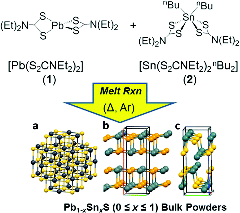 | ||
| Fig. 1 Synthetic pathway to produce Pb1−xSnxS (0 ≤ x ≤ 1) alloys from solventless reactive melt themolysis of (1) and (2). Crystal structures relevant to this study; (a) galena, PbS (a = b = c = 5.94 Å; α = β = γ = 90°; space group Fm3m). (b) Teallite, PbSnS2, (a = 11.3 Å; b = 4.05 Å; c = 4.4 Å; α = β = γ = 90°, viewed in the ‘armchair’ direction). (c) Herzenbergite SnS (a = 3.98 Å; b = 4.33 Å; c = 11.18 Å; α = β = γ = 90°; space group Pmcn, viewed in the ‘zig zag’ direction). Dark spheres correspond to metal atoms, yellow spheres correspond to sulfur atoms in all cases. | ||
Results and discussion
In a typical procedure, powders of 1 and 2 are pre mixed at stoichiometric ratios to produce Pb1−xSnxS alloys according to the target composition (x = 0, 0.2, 0.4, 0.5, 0.6, 0.8 and 1.0) using a mortar and pestle, and are then placed in a ceramic boat. The mixed precursors are heated to 450 °C at a rate of 20 °C min−1 in a temperature controlled furnace under an argon atmosphere and held at this temperature for 1 h before cooling to RT and are then discharged from the furnace to leave grey-black powders in all cases. According to the melting points of 1 and 2 (89 and 208 °C respectively), melting and mixing of the precursors in the liquid phase at the atomic scale prior to decomposition will occur. According to the thermogravimentric analysis (TGA) profiles of 1 and 2, at > 350 °C decomposition of the dithiocarbamate complexes occurs to yield the metal chalcogenide alloys. These two features pre-dispose the system to random and homogeneous alloying at the atomic scale, and resists the propensity toward phase separation.Powder X-ray diffraction (pXRD) was used to gain information regarding the crystal structures of the alloys synthesized (Fig. 2). The end members of the alloy series, PbS and SnS could be matched well to ICCD patterns for cubic galena and orthorhombic herzenbergite respectively. The diffraction patterns of the alloys showed a progression from cubic type structure to orthorhombic type structures. A plot of the (111) d-spacing vs. the amount of Sn in the structure (i.e. x) revealed that at around x = 0.5 there is a significant break from the cubic structures found for x = 0, 0.2. and 0.4 and for values x ≥ 0.5 there is a step change in the value of d111 from ca. 3.3–3.4 Å to 2.8–2.9 Å. This can be envisaged as the expansion of the c axis and the contraction of the a and b axes in going from cubic (i.e. the PbS halite type structure) to the orthorhombic layer structure of SnS/PbSnS2.27
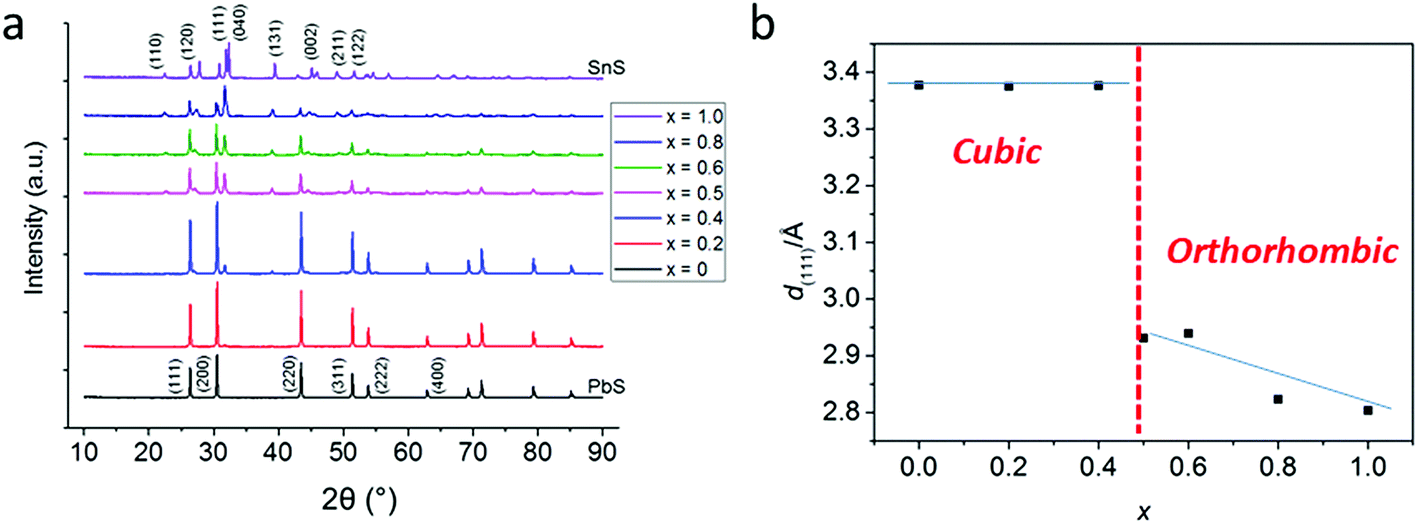 | ||
| Fig. 2 pXRD analysis of bulk Pb1−xSnxS (0 ≤ x ≤ 1) alloys. (a) Offset diffraction patterns of bulk Pb1−xSnxS (0 ≤ x ≤ 1) with major (hkl) reflections labelled. (b) Analysis of the d111 spacing as a function of compositional variation (x). The red dash line shows the transition between cubic structures and orthorhombic structures. | ||
Scanning electron microscopy was used to investigate the morphology of the materials produced from melt thermolysis of precursors (Fig. 3). Microcrystalline material was produced in all cases. The results of the SEM analysis mirrored that of the pXRD patterns; alloys with 0 ≤ x ≤ 0.4 had definite cubic morphologies, whilst alloys with x ≥ 0.5 displayed platy morphologies typical of materials with layered structures e.g. SnS, which tend to grow preferentially in 2 dimensions due to the enthalpic payoff of creating more ionic bonds in this direction as opposed to vertical growth which includes galleries held together by weaker van der Waals forces. EDX spectroscopy of the bulk alloys demonstrated that a smooth elemental transition between Pb and Sn was possible using this synthetic method with potentially excellent control of alloying. EDX spectrum mapping of the powders over a wide area (ca. 9 mm2) with maps constructed for Pb, Sn and S show that the alloys are elementally uniform, as the signals for each element are co-localized in space in the images, and also correspond to the morphological features of the secondary electron images of the powders taken in parallel, even at higher magnifications where mapping of single crystallites could be performed (ESI images in S4 and S5†). This confirms that there is no phase separation of the materials across the length scales.
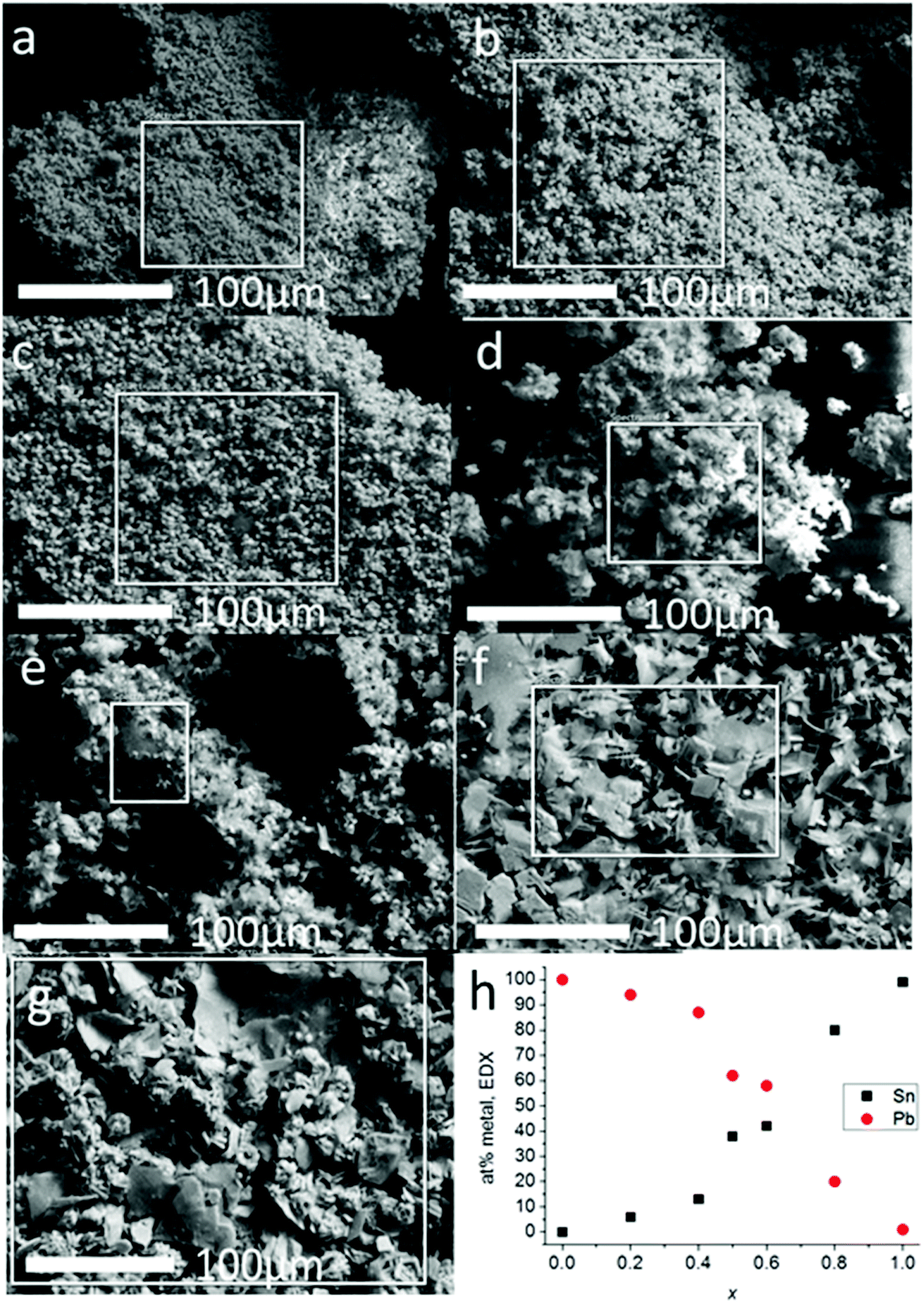 | ||
| Fig. 3 Secondary electron SEM images (6 kV) of bulk Pb1−xSnxS (0 ≤ x ≤ 1) alloys. (a) x = 0 (i.e. PbS); (b) x = 0.2 (c), x = 0.4 (d) x = 0.5 (e) x = 0.6 (f) x = 0.8 (g) x = 1.0 (i.e. SnS). (h) at% of Sn and Pb found by EDX spectroscopy within the square areas of each image plotted as a function of compositional variation (x). | ||
Raman spectroscopy was used to further confirm alloying (Fig. 4). The spectrum for PbS is typical of that of unoriented bulk galena (PbS) with optical modes observed at 75, 130 and 177 cm−1. The peak at 130 cm−1 has a shoulder at around 108 cm−1. The form of this spectrum is maintained over the alloy range 0 ≤ x ≤ 0.4 which agrees well with the pXRD data that suggests a cubic crystal structure is maintained for these alloys. Alloys where 0.5 ≤ x ≤ 1 take more the form of the end compound SnS, and have the appearance of the Raman spectrum for unoriented herzenbergite, which has 12 Raman active bands (4Ag, 2B1g, 4B2g, and 2B3g) and in theory all phonon modes should be observed simultaneously. Hence, for 2-D The Raman spectrum of the SnS (x = 1.0) on a silicon substrate displays two broad bands with peak maxima at 150 and 220 cm−1 The small peak around 300 cm−1 is tentatively assigned to the B2g optical mode of SnS.
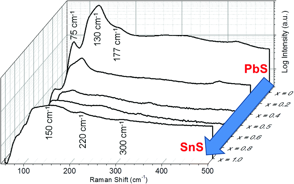 | ||
| Fig. 4 Raman spectra for bulk Pb1−xSnxS (0 ≤ x ≤ 1) alloys demonstrating the transition between PbS (x = 0) through to SnS (x = 1.0). Spectra are offset in 3D and plotted against compositional variation (x). n.b. x = 0.2 and x = 0.8 have been removed for clarity, but can be viewed in the ESI.† | ||
In summary, the characterisation performed on the Pb1−xSnxS alloys where x = 0.6, 0.8 and 1.0 confirmed that they were crystalline with a layered orthorhombic structure. The stability of Pb0.2Sn0.8S bulk material and as a monolayer was also estimated by a thermodynamic model that is based on DFT calculations (ESI†). The temperature dependence of the Gibbs free energy of mixing Gmix was calculated as shown in Fig. 5. It is defined as:
| Gmix = Hmix − TSmix, | (1) |
Smix = −kB(x![[thin space (1/6-em)]](https://www.rsc.org/images/entities/char_2009.gif) lnx + (1 − x)ln(1 − x)), lnx + (1 − x)ln(1 − x)), | (2) |
| Hmix = E(Pb1−xSnxS) − (1 − x)E(PbS) − xE(SnS), | (3) |
 | (4) |
 | ||
| Fig. 5 Calculated thermodynamic stability of Pb0.2Sn0.8S alloy. Plot of the Gibbs free energy of mixing Gmix for a Pb0.2Sn0.8S alloy versus temperature in kelvins as calculated by a thermodynamic model in bulk and in monolayer. The result suggests that mixing of PbS and SnS is unfavourable at T = 0 K, but at the temperature of synthesis of the bulk alloys (723 K) and room temperature (298 K), mixing is thermodynamically favourable. | ||
At T = 0 K, a positive Gibbs free energy of mixing was calculated for both the bulk material and monolayer material, indicating that phase separation into SnS and PbS is more favourable than alloying. However, Gmix decreases upon increasing temperature, so that at both room temperature (ca. 298 K), and the synthesis temperature (723 K), negative values for Gmix are obtained, which indicates that the Pb0.2Sn0.8S is a thermodynamically favourable product in both bulk (QED), but importantly also in monolayer form.
We further calculated with DFT the cleavage energy of Pb0.2Sn0.8S to be 31 meV Å−2 (33 meV Å−2 for SnS) as difference in adhesion between a monolayer and the corresponding bulk crystal. These values are similar to other layer structures which can be exfoliated to 2D materials.33 We therefore hypothesised then that these materials could be exfoliated to nanoscale dimensions in the 2D limit.
Liquid phase exfoliation (LPE) provides a facile route to the thinning of layered materials to produce colloids of nanosheets and importantly is a scalable methodology. Indeed, we reported LPE by exfoliation of bulk commercially available SnS in N-methyl pyrollidine (NMP) to produce SnS nanosheets previously. Here, we focused on the synthesis and characterisation of Pb0.2Sn0.8S nanosheets as an exemplar route towards a 2D material using our synthetic alloy feedstock, which is non-extant in nature and unavailable from commercial suppliers. The appearance of Pb0.2Sn0.8S at higher magnifications in the SEM as platy crystals (ESI†), combined with its orthorhombic structure confirmed by PXRD suggested that this material would be suitable for exfoliation. Therefore the Pb0.2Sn0.8S powder produced from thermolysis was immersed in NMP and ultrasonicated at moderate energy for 24 h with temperature control to avoid extensive degradation of sheets as-recommended by Coleman and co-workers.34 Purification by a centrifugation step to remove unexfoliated bulk material was performed before further analysis. In all cases, stable colloids were produced, which had a dark turbid appearance.
Pb0.2Sn0.8S nanosheets were analysed by scanning electron microscopy (SEM) to determine the lateral sizes of the material produced. Typical secondary electron images of nanosheets taken at 6 kV are shown in Fig. 6. From SEM data it was possible to produce histograms of longest and shortest sides of sheets thus it was also possible to produce a histogram of the aspect ratio observed (N = 50). Pb0.2Sn0.8S nanosheets had a mean length of 134 ± 81 nm, with a mean width of 85 ± 45 nm and a mean aspect ratio of 1.6 ± 0.5. Thus it may be surmised that the sheets tend to be elongated which may imply that there is unequal rate of shear between basal plane atoms during exfoliation possibly due to the anisotropic crystal structure, which has armchair and zig zag directions as per black phosphorus.
 | ||
Fig. 6 Lateral size and shape analysis of Pb0.2Sn0.8S nanosheets by SE SEM (N = 50). (a) Typical SE SEM image (6 kV) of nanosheets deposited by drop casting of the colloidal solution onto Si@SiO2 substrates. (b) Histogram showing length distribution of Pb0.2Sn0.8S nanosheets, with normal distribution overlayed (![[x with combining macron]](https://www.rsc.org/images/entities/i_char_0078_0304.gif) ± σ = 134 ± 81 nm). (c) Histogram showing width distribution of Pb0.2Sn0.8S nanosheets, with normal distribution overlayed ( ± σ = 85 ± 45 nm). (d) Histogram showing aspect ratio of Pb0.2Sn0.8S nanosheets, with normal distribution overlayed ( ± σ = 1.6 ± 0.5). ± σ = 134 ± 81 nm). (c) Histogram showing width distribution of Pb0.2Sn0.8S nanosheets, with normal distribution overlayed ( ± σ = 85 ± 45 nm). (d) Histogram showing aspect ratio of Pb0.2Sn0.8S nanosheets, with normal distribution overlayed ( ± σ = 1.6 ± 0.5). | ||
High angle annular dark field scanning transmission microscopy (HAADF STEM) was used to investigate Pb0.2Sn0.8S sheets at the nanoscale. A typical nanosheet is shown in Fig. 7. It appears bright on the dark background due to the z contrast afforded by collection of the signal with the HAADF detector. The sheets generally appear crystalline with well-defined edges, and as the statistics from SEM images suggested are below 200 × 200 nm length and width, with aspect ratios above 1.0. EDX spectrum mapping of the materials at the same scale reveals the homogeneous distribution of lead and tin ions throughout the nanosheet (Fig. 7).
 | ||
| Fig. 7 Characterisation of 2D Pb0.2Sn0.8S with electron microscopy: BF-TEM, HAADF STEM imaging and EDX spectrum maps of Pb0.2Sn0.8S nanosheets (200 kV). (a) BF-TEM image of a large nanosheet. (b) HAADF STEM image of the same Pb0.2Sn0.8S nanosheet as found in (a). (c) HAADF STEM image of a Pb0.2Sn0.8S nanosheet. (d) EDX spectrum image of the sulfur Kα line (2.31 keV). (e) EDX spectrum image of the Sn Lα line (3.44 keV). (f) EDX spectrum image of the Pb Lα line (10.6 keV). | ||
The thickness of the Pb0.2Sn0.8S nanosheets was investigated by atomic force microscopy (AFM). It was found that the average thickness for flakes (N = 100) was ca. 10.9 ± 7.7 nm, corresponding to approximately 20 atomic layers given the bulk lattice constant for SnS c = 11.18 Å. A histogram of the measurement is shown in Fig. 8. 55% of the flakes surveyed are <10 nm, and it is apparent from the histogram that a large amount of flakes are probably few-layer at this point.
 | ||
| Fig. 8 AFM analysis of Pb0.2Sn0.8S nanosheets (N = 100). (a) High magnification height image of Pb0.2Sn0.8S nanosheets. (b) Low magnification AFM height of Pb0.2Sn0.8S nanosheets. (c) Histogram of thicknesses of Pb0.2Sn0.8S sheets with a normal distribution overlayed ( ± σ = 10.9 ± 7.7 nm). | ||
With further high speed centrifugation (11620g) followed by rejection of the pellet formed and retaining the supernatant, it was possible to thin the sheets to near atomic dimensions. Analysis of this sample by AFM revealed much lower flake thicknesses on average (2.7 ± 1.7 nm, corresponding to ca. 4–5 atomic layers), and the flakes look to be predominatly few-layer. High resolution scans of single flakes allowed accurate step height measurement. The example in Fig. 9(c) shows the image of a single flake, with a step height measured corresponding to around 0.2 nm, which, may be a monolayer flake within the error of the measurement.
 | ||
| Fig. 9 AFM analysis of Pb0.2Sn0.8S nanosheets (N = 100) after high speed centrifugation. (a) Low magnification height image of Pb0.2Sn0.8S nanosheets. (b) Histogram of thicknesses of Pb0.2Sn0.8S sheets with a normal distribution overlayed ( ± σ = 2.7 ± 1.7 nm). (c) High resolution image of Pb0.2Sn0.8S nanosheets. (d) Step height measurement of a single flake. Inset: high magnification AFM height of a single Pb0.2Sn0.8S nanosheet. The step height measurement shown in (d) was performed along the white line superimposed over the image. | ||
The band gap energies of SnS and a structurally similar, layered modification of PbS (reported as a PbS high-pressure modification35) were calculated (ESI†) for monolayers, bilayers and bulk crystals employing the HSE06 hybrid functional (star symbols in Fig. 10(a)). We used HSE06 because band gaps are in better agreement with experimental values than those obtained with the PBE functional that is commonly employed for the analysis of crystalline structures.36 For these systems a comparison with the band gaps obtained with PBE showed that the HSE06 values are obtained by scaling the PBE results by a factor of 1.48 (with a standard deviation of 0.11). The band gaps for Pb0.2Sn0.8S were then obtained from PBE and scaled accordingly (HSE06 calculations for alloys are not feasible because their unit cells are too large). For each system the obtained data points are then fitted to the following scaling law (continuous lines in Fig. 10(a)):
| Eg(N) = aNb + Eg(bulk) | (5) |
 | ||
| Fig. 10 Optical characterisation of Sn0.8Pb0.2S. (a) Calculated band gap energies of Sn0.8Pb0.2S, SnS, and layered PbS as a function of layer number. (b) Tauc plots of (αhν)2vs. hν over the vis-NIR range of the electromagnetic spectrum, estimating direct optical band gaps of 1.25 eV for a standard Sn0.8Pb0.2S sol (black line) and 1.86 eV for the supernatant from a sol subjected to high speed centrifugation (11600g, red line) respectively. | ||
UV-Vis absorption spectroscopy was used to assess the band gap of bulk Pb0.2Sn0.8S nanosheets by experiment (Fig. 10(b)). It was found that the colloid has a large featureless absorbance that extends from the NIR region of the electromagnetic spectrum through the entirety of the visible range, hence the black colour of the sol (ESI†). Analysis of this data furthermore revealed that the material has a direct band gap of 1.25 eV due to the exponent of 2 in the Tauc plot ordinate.37 Upon thinning of the material via high speed centrifugation, the band gap of the material increases to 1.86 eV. These measurements agree well with the calculations in terms of the upward energy trend observed; as bulk Pb0.2Sn0.8S alloys are thinned to nanoscale dimensions, the band gap increases markedly. Within the limits of the numerical approximations, a range of energies between 1.3 eV and 2.1 eV could potentially be obtained therefore for Pb0.2Sn0.8S nanosheets, presumably by controlling thickness, for example with cascade centrifugation.
There is also another striking consequence of alloying in the Pb0.2Sn0.8S system: the band gap changes from being indirect in nature for SnS (i.e. requiring a change in crystal momentum for the transition) to a direct band gap material in Pb0.2Sn0.8S. This is a remarkable result given the minority amount of lead in the host lattice, yet a theoretical analysis reveals why this is the case. Investigation of the nature of the calculated density of states for Pb0.2Sn0.8S near to the Fermi level suggest that there is no significant contribution from Pb-based orbitals at the conduction and valence band edges; the band edge states are predominantly formed from contributions by Sn and S atoms (ESI†). However the inclusion of 20% Pb into SnS leads to a sizable structural deformation of the in-plane lattice, where the bulk lattice parameter A increases by 2% and the lattice parameter B decreases by 1% (ESI†). These structural changes alter the energy of band edge states and turn the system into a direct band gap material. This is illustrated in Fig. 11 that shows the calculated energies of valence band and conduction band states along relevant high-symmetry lines in the Brillouin zone. The transition from an indirect band gap in SnS (Fig. 11(a)) to a direct gap in Pb0.2Sn0.8S is clearly discernible. Due to the negligible contribution of Pb states near the band edges, Pb0.2Sn0.8S is modelled as structurally deformed SnS in Fig. 11.
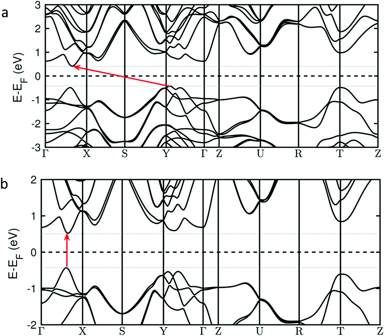 | ||
| Fig. 11 Calculated band structures for bulk crystals of (a) SnS and (b) SnS in the Pb0.2Sn0.8S structure. The horizontal dashed lines show the Fermi energies and the red arrows the HOCO–LUCO excitations. HOCO (highest occupied crystal orbital) and LUCO (lowest unoccupied crystal orbital) are the edges of the valence and conduction bands respectively. The Fermi energy is set to zero. | ||
Conclusions
A scalable reaction pathway has been developed that can produce a full series of bulk alloys of the form Pb1−xSnxS (0 ≤ x ≤ 1) based on the decomposition of molecular metal dithiocarbamate complexes at relatively low temperature without the use of solvents. The stability of the aforementioned materials at room temperature in the layered form is predicted by DFT, and confirmed by pXRD measurements that suggest a cubic to orthorhombic transition at x = 0.5. Subsequent liquid phase exfoliation of an exemplar alloyed layered material, Pb1−xSnxS (x = 0.8) demonstrates the production of alloyed 2D nanosheets from this reaction is possible. The thickness-dependent optical band gaps of the sheets agree well with trends obtained from DFT calculations using hybrid-functionals and are predicted to be in the range 1.3–2.1 eV. There is a striking change from an indirect band gap for SnS to a direct band gap for Pb0.2Sn0.8S which we believe is caused by strong changes in the crystallographic parameters. The latter is an important finding of the study; the change from indirect to direct band gap materials allows for more light to be absorbed, which could be important for a range of applications, most notably thin film solar devices. Given that these materials are solution processable there may be a wide scope for the production of printable electronic devices, given the potential of SnS in these areas.A further, more generally profound conclusion of the study is that we have developed a scalable pathway toward new synthetic bulk layered materials. The melt reactions proposed here could be adapted to produce a range of layered materials e.g. MoS2, WS2, using metal dithiocarbamate complexes, of which there are myriad.38 The limiting factor for most exfoliation processes is the availability of layered bulk material. With only a number of feedstocks available in bulk (e.g. graphite, hBN, MoS2, WS2) the palette of 2D materials is inherently limited. However, the work we present here opens the door to design a range of bespoke designed bulk materials that can be exfoliated into 2D materials with advanced, tunable properties e.g. alloys, doped materials with robust room temperature magnetic properties. We are currently exploring these avenues.
Conflicts of interest
There are no conflicts to declare.Acknowledgements
K. J. N. is funded by a DTA EPSRC studentship awarded to the University of Manchester. S. J. M. is funded by an EPSRC Doctoral Prize. N. Z. is funded by a donor research impact scholarship. J. K. and G. S. acknowledge funding by the German Research Foundation (DFG) under grant number SE 651/45-1. Computational resources for this project were provided by ZIH Dresden. We thank Professor Paul O'Brien CBE FRS (22nd Jan 1954–16th Oct 2018) for useful discussions; this paper is dedicated to his memory.References
- K. S. Novoselov, A. K. Geim, S. V. Morozov, D. Jiang, Y. Zhang, S. V. Dubonos, I. V. Grigorieva and A. A. Firsov, Science, 2004, 306, 666–669 CrossRef CAS PubMed.
- P. Miro, M. Audiffred and T. Heine, Chem. Soc. Rev., 2014, 43, 6537–6554 RSC.
- T. Heine, Acc. Chem. Res., 2015, 48, 65–72 CrossRef CAS PubMed.
- K. Novoselov, D. Jiang, F. Schedin, T. J. Booth, V. V. Khotkevich, S. V. Morosov and A. K. Geim, Proc. Natl. Acad. Sci. U. S. A., 2005, 102, 10451–10453 CrossRef CAS PubMed.
- P. Blake, P. D. Brimicombe, R. R. Nair, T. J. Booth, D. Jiang, F. Schedin, L. A. Ponomarenko, S. V. Morozov, H. F. Gleeson, E. W. Hill, A. K. Geim and K. S. Novoselov, Nano Lett., 2008, 8, 1704–1708 CrossRef PubMed.
- Y. Hernandez, V. Nicolosi, M. Lotya, F. M. Blighe, Z. Sun, S. De, I. T. McGovern, B. Holland, M. Byrne, Y. K. Gun'Ko, J. J. Boland, P. Niraj, G. Duesberg, S. Krishnamurthy, R. Goodhue, J. Hutchison, V. Scardaci, A. C. Ferrari and J. N. Coleman, Nat. Nanotechnol., 2008, 3, 563 CrossRef CAS PubMed.
- H. Tao, Y. Zhang, Y. Gao, Z. Sun, C. Yan and J. Texter, Phys. Chem. Chem. Phys., 2017, 19, 921–960 RSC.
- A. Harvey, J. B. Boland, I. Godwin, A. G. Kelly, B. M. Szydłowska, G. Murtaza, A. G. Thomas, D. J. Lewis, P. O'Brien and J. N. Coleman, 2D Mater., 2017, 4, 025054 CrossRef.
- J. N. Coleman, M. Lotya, A. O'Neill, S. D. Bergin, P. J. King, U. Khan, K. Young, A. Gaucher, S. De, R. J. Smith, I. V. Shvets, S. K. Arora, G. Stanton, H. Y. Kim, K. Lee, G. T. Kim, G. S. Duesberg, T. Hallam, J. J. Boland, J. J. Wang, J. F. Donegan, J. C. Grunlan, G. Moriarty, A. Shmeliov, R. J. Nicholls, J. M. Perkins, E. M. Grieveson, K. Theuwissen, D. W. McComb, P. D. Nellist and V. Nicolosi, Science, 2011, 331, 568–571 CrossRef CAS PubMed.
- A. A. Tedstone, J. R. Brent and D. J. Lewis, in Nanoscience, The Royal Society of Chemistry, 2017, vol. 4, pp. 108–141 Search PubMed.
- K. F. Mak, C. Lee, J. Hone, J. Shan and T. F. Heinz, Phys. Rev. Lett., 2010, 105, 136805 CrossRef PubMed.
- J. Suh, T.-E. Park, D.-Y. Lin, D. Fu, J. Park, H. J. Jung, Y. Chen, C. Ko, C. Jang, Y. Sun, R. Sinclair, J. Chang, S. Tongay and J. Wu, Nano Lett., 2014, 14, 6976–6982 CrossRef CAS PubMed.
- A. Ramasubramaniam and D. Naveh, Phys. Rev. B, 2013, 87, 195201 CrossRef.
- D. O. Dumcenco, K. Y. Chen, Y. P. Wang, Y. S. Huang and K. K. Tiong, J. Alloys Compd., 2010, 506, 940–943 CrossRef CAS.
- J. Zhou, J. Lin, X. Huang, Y. Zhou, Y. Chen, J. Xia, H. Wang, Y. Xie, H. Yu, J. Lei, D. Wu, F. Liu, Q. Fu, Q. Zeng, C.-H. Hsu, C. Yang, L. Lu, T. Yu, Z. Shen, H. Lin, B. I. Yakobson, Q. Liu, K. Suenaga, G. Liu and Z. Liu, Nature, 2018, 556, 355–359 CrossRef CAS PubMed.
- Z. Lin, Y. Liu, U. Halim, M. Ding, Y. Liu, Y. Wang, C. Jia, P. Chen, X. Duan, C. Wang, F. Song, M. Li, C. Wan, Y. Huang and X. Duan, Nature, 2018, 562, 254–258 CrossRef PubMed.
- J. Wang, X. Cai, R. Shi, Z. Wu, W. Wang, G. Long, Y. Tang, N. Cai, W. Ouyang, P. Geng, B. N. Chandrashekar, A. Amini, N. Wang and C. Cheng, ACS Nano, 2018, 12, 635–643 CrossRef PubMed.
- M. A. R. Anjum, H. Y. Jeong, M. H. Lee, H. S. Shin and J. S. Lee, Adv. Mater., 2018, 30, 1707105 CrossRef PubMed.
- W. Fang, H. Zhao, Y. Xie, J. Fang, J. Xu and Z. Chen, ACS Appl. Mater. Interfaces, 2015, 7, 13044–13052 CrossRef CAS PubMed.
- J. R. Brent, D. J. Lewis, T. Lorenz, E. A. Lewis, N. Savjani, S. J. Haigh, G. Seifert, B. Derby and P. O'Brien, J. Am. Chem. Soc., 2015, 137, 12689–12696 CrossRef CAS PubMed.
- Z. Tian, C. Guo, M. Zhao, R. Li and J. Xue, ACS Nano, 2017, 11, 2219–2226 CrossRef CAS PubMed.
- C. Xin, J. Zheng, Y. Su, S. Li, B. Zhang, Y. Feng and F. Pan, J. Phys. Chem. C, 2016, 120, 22663–22669 CrossRef CAS.
- L. Medrano Sandonas, D. Teich, R. Gutierrez, T. Lorenz, A. Pecchia, G. Seifert and G. Cuniberti, J. Phys. Chem. C, 2016, 120, 18841–18849 CrossRef CAS.
- P. Z. Hanakata, A. Carvalho, D. K. Campbell and H. S. Park, Phys. Rev. B, 2016, 94, 035304 CrossRef.
- S. Karmakar, C. Chowdhury and A. Datta, J. Phys. Chem. C, 2016, 120, 14522–14530 CrossRef CAS.
- C. Chowdhury, S. Karmakar and A. Datta, J. Phys. Chem. C, 2017, 121, 7615–7624 CrossRef.
- L. L. Chang and W. R. Brice, Mineral. Mag., 1971, 38, 186–189 CrossRef CAS.
- T. Baak, E. D. Dietz, M. Shouf and J. A. Walmsley, J. Chem. Eng. Data, 1966, 11, 587–588 CrossRef CAS.
- N. Al-Dulaimi, D. J. Lewis, X. L. Zhong, M. Azad Malik and P. O'Brien, J. Mater. Chem. C, 2016, 4, 2312–2318 RSC.
- D. J. Lewis, A. A. Tedstone, X. L. Zhong, E. A. Lewis, A. Rooney, N. Savjani, J. R. Brent, S. J. Haigh, M. G. Burke, C. A. Muryn, J. M. Raftery, C. Warrens, K. West, S. Gaemers and P. O'Brien, Chem. Mater., 2015, 27, 1367–1374 CrossRef CAS.
- A. A. Tedstone, E. A. Lewis, N. Savjani, X. L. Zhong, S. J. Haigh, P. O'Brien and D. J. Lewis, Chem. Mater., 2017, 29, 3858–3862 CrossRef CAS.
- N. Al-Dulaimi, E. A. Lewis, D. J. Lewis, S. K. Howell, S. J. Haigh and P. O'Brien, Chem. Commun., 2016, 52, 7878–7881 RSC.
- T. Björkman, A. Gulans, A. V. Krasheninnikov and R. M. Nieminen, Phys. Rev. Lett., 2012, 108, 235502 CrossRef PubMed.
- C. Backes, T. M. Higgins, A. Kelly, C. Boland, A. Harvey, D. Hanlon and J. N. Coleman, Chem. Mater., 2017, 29, 243–255 CrossRef CAS.
- T. Chattopadhay, A. Werner, H. G. von Schnering and J. Pannetier, Rev. Phys. Appl., 1984, 19, 807–813 CrossRef.
- Y.-S. Kim, K. Hummer and G. Kresse, Phys. Rev. B, 2009, 80, 035203 CrossRef.
- J. Tauc, Mater. Res. Bull., 1968, 3, 37–46 CrossRef CAS.
- G. Hogarth, in Progress in Inorganic Chemistry, 2005, DOI:10.1002/0471725587.ch2.
Footnotes |
| † Electronic supplementary information (ESI) available. See DOI: 10.1039/c8sc04018d |
| ‡ These authors contributed equally. |
| This journal is © The Royal Society of Chemistry 2019 |