
 Open Access Article
 This Open Access Article is licensed under a Creative Commons Attribution-Non Commercial 3.0 Unported Licence
P3HT-based visible-light organic photodetectors using PEI/PAA multilayers as a p-type buffer layer†
Chan Hyuk Ji,
Seon Ju Lee and
Se Young Oh *
*
Department of Chemical and Biomolecular Engineering, Sogang University, Seoul 04107, Republic of Korea. E-mail: syoh@sogang.ac.kr
First published on 13th November 2019
Abstract
A low leakage current is critical for achieving organic photodetectors (OPDs) with high detectivity. The insertion of buffer layers is an effective approach for reducing the reverse-biased leakage current. In this study, polyelectrolyte multilayers comprising polyethyleneimine (PEI) and polyacrylic acid (PAA) were introduced by a spin-assisted layer-by-layer technique into an OPD as a p-type buffer layer. Although PEI/PAA multilayers are insulators, when used as a buffer layer in our device, they suppressed the leakage current and also provided a high photocurrent due to the light-assisted tunneling effect. The prepared device configuration was ITO/(PEI/PAA)2/P3HT:PC60BM/Yb/Al. The performances of the OPDs were investigated by measuring the current–voltage characteristics, external quantum efficiency, and transient photocurrent. In addition, the operating mechanism of the OPDs was confirmed by impedance analysis. The device comprising (PEI/PAA)2 showed a specific detectivity of 3.11 × 10¹² Jones and a bandwidth of 103.2 kHz at −1 V and 525 nm. This performance is a numerical value that can be used in devices such as a line scan camera. In addition, because this device is fabricated by a low-temperature solution process, flexible and large-area substrates can be used.
Introduction
Photodetectors that convert incident photons into an electrical signal are prevalent in consumer electronics, mobile devices, vehicle systems, military applications, and security.1,2 Traditionally, most commercial photodetectors are based on inorganic materials such as silicon and III–V compounds that have been developed owing to their high charge-carrier mobility, small exciton binding energy, and high stability.3 However, inorganic-based photodetectors have limited use in advanced applications such as augmented reality and autonomous running, where a suitable design and miniaturization is required, because of the complicated manufacturing processes and mechanical inflexibility.4In recent years, many studies have been conducted to replace inorganic photodetectors by utilizing organic materials having a high adsorption coefficient, mechanical flexibility, adjustable energy levels, and the possibility of large-area fabrication and solution processing.5–7 In particular, polymer–fullerene blends have attracted great interest as active materials in organic photodetectors (OPDs) in the visible-light region,8,9 and poly(3-hexylthiophene-2,5-diyl):[6,6]-phenyl-C61-butyric acid methyl ester (P3HT:PC60BM) is widely used as a photoactive material.10–13 With these materials, a p-type/n-type buffer layer is inserted between the active layer and the electrodes to improve the device performance. Some devices are operated under reverse bias to achieve the required response speed and bandwidth for certain applications such as line scan cameras (100 kHz) and optical communication (1 MHz).13–15 Under the applied reverse bias, carriers flow into the active layer from the electrode, thereby generating a leakage current.
A low leakage current is important for using an organic photodetector with high detectivity and the charge-blocking ability of the inserted buffer layer substantially contributes in inhibiting the reverse-bias leakage current. Poly(3,4-ethylenedioxythiophene):poly(styrenesulfonate) (PEDOT:PSS)9,11 and NiOx16 are widely used as p-type buffer layers in the solution process. However, OPDs using the PEDOT:PSS layer encounter problems such a high dark current under reverse bias and device instability.17 Moreover, the NiOx layer normally requires a high-temperature (>300 °C) sintering process to enable efficient carrier transport, which makes the application of a flexible substrate difficult.18 Insulator materials as an ultra-thin (1–2 nm) buffer layer are also used in organic solar cells to suppress the recombination of carriers separated from the excitons.19 However, for OPDs in which only an ultra-thin insulator is used as a buffer layer without another blocking layer, electrons can pass through the insulator layer due to a direct tunneling effect and the suppression of leakage current caused by the reverse voltage becomes difficult.20
In this work, we introduced polyelectrolyte multilayers comprising polyethyleneimine (PEI) and polyacrylic acid (PAA) by a spin-assisted layer-by-layer (LBL) technique21 into a P3HT:PC60BM-based OPD as a p-type buffer layer. PEI/PAA multilayers fabricated by the LBL process are used in various fields such as biomedicine,22 membrane technology,23 and insulators for organic transistors24–26 because it is possible to control the thickness at a molecular level and to fabricate a pinhole-free thin film. However, to the best of our knowledge, PEI/PAA multilayers have not been used in photodetectors as p-type buffer layers because of their poor charge-transport ability (i.e., insulator). Wang et al.49 used a PEIE insulator as a p-type buffer layer, which created an energy barrier and increased the tunneling current due to accumulated charge, resulting in a high EQE. However, the specific detectivity was 1.01 × 10¹² Jones due to the high dark current. In this study, we achieved a detectivity that was three times higher and a dark current two orders lower than the values presented by Wang et al. The PEI/PAA multilayers allow for thickness control without introducing pinholes, effectively reducing the dark current in the corresponding devices. In addition, PEI/PAA multilayers produced using the LBL process have higher dielectric polarization due to the ordered dipoles than a single PEIE film, thereby accumulating more charge under reverse bias.50 Herein, we compare the performance of OPDs developed using the PEI/PAA multilayers with that of the devices using PEDOT:PSS or NiOx as a p-type buffer layer. In addition, the transient photocurrent was measured to investigate the response speed of the device, and the resistance and capacitance were measured through impedance measurement to analyze the light-assisted tunneling property.
Experiments
Materials and reagents
PEI (branched, Mw ∼ 25![[thin space (1/6-em)]](https://www.rsc.org/images/entities/char_2009.gif) 000), PAA (Mw ∼ 100000 and Mv ∼ 450000), P3HT, and nickel(II) acetate tetrahydrate (≥99.0% purity) were purchased from Sigma-Aldrich Co., Ltd. PC60BM was obtained from Nano-C, PEDOT:PSS (Clevious PH 1000) was purchased from Heraeus, and ytterbium (Yb) and aluminum (Al) as ETL materials were obtained from iTASCO. The other chemicals used were of reagent grade.
000), PAA (Mw ∼ 100000 and Mv ∼ 450000), P3HT, and nickel(II) acetate tetrahydrate (≥99.0% purity) were purchased from Sigma-Aldrich Co., Ltd. PC60BM was obtained from Nano-C, PEDOT:PSS (Clevious PH 1000) was purchased from Heraeus, and ytterbium (Yb) and aluminum (Al) as ETL materials were obtained from iTASCO. The other chemicals used were of reagent grade.
Fabrication of organic photodetectors (OPDs)
Patterned ITO (≤20 Ω sq−1) glass substrates were sequentially cleaned in an ultrasonic bath of acetone, isopropyl alcohol, and deionized water for 15 min each, and then treated by UV/ozone for 15 min. The spin-assisted LBL method was carried out following the procedure reported by Ma et al.21 Briefly, several drops of PAA (1 mg mL−1, pH = 6.5) or PEI (1 mg mL−1, pH = 6.5) solution were placed on the substrate surface and the substrate was rotated at a speed of 4000 rpm for 15 s. After the assembly of each polyelectrolyte layer, the substrate was washed by placing several drops of deionized water and spinning the substrate at the same speed and holding time as those used for layer deposition. The above steps constitute one complete cycle of deposition. By repeating this cycle (1–4 times), a multilayer film was obtained, which is denoted as (PEI/PAA)n (PAA terminated), where n represents the number of deposition cycles. In two-component systems (PEI and PAA), the deposition of both the components is referred to as a bilayer (i.e., 1 complete cycle = 1 bilayer).The LBL films were annealed at 120 °C for 10 min on a hot plate. A solution of P3HT:PC60BM (1:0.8) in chlorobenzene (10 mg mL−1) was spin-cast at 600 rpm onto the LBL thin film and annealed at 120 °C for 10 min on the hot plate. Finally, Yb (2 nm) and Al (100 nm) were deposited by a thermal evaporation technique at 10−6 torr (ULVAC VTR-300M/1ERH evaporator, Japan). The active area thus obtained was ∼0.04 cm2.
To form a NiOx film (15 nm),18 nickel(II) acetate tetrahydrate was dissolved in 2-methoxyethanol (0.1 M) by sonication. The prepared nickel oxide solution was coated on the ITO glass substrates by spin coating at 4000 rpm for 45 s and annealing at 400 °C for 30 min. To form the PEDOT layer (30 nm)14 on the ITO, PEDOT was deposited by spin coating at 5000 rpm for 45 s and annealed at 150 °C for 10 min.
Device characteristics
Current–voltage and impedance measurements were performed under the illumination of monochromatic light from a light-emitting diode (525 nm, 1 mW cm−2) using an Iviumstat (Ivium Technologies, Netherlands). The external quantum efficiency (EQE) was measured using a spectral incident photon-to-electron conversion efficiency (IPCE) system (SpectraPro 300i, Acton Research Co., Ltd). The film thickness was measured using a spectroscopic ellipsometer (Woollam Co., USA). The transient photocurrent (TPC) and dynamic characteristics were measured using a photoresponse measurement system (TNE Tech Co., Ltd, South Korea). The light-emitting diode (525 nm) in the photoresponse measurement system was modulated by a function generator to act as an excitation source. Square waves with different frequencies were applied. The photodetectors were directly connected to an oscilloscope (Tektronix TDS 3012B) with an input impedance of 50 Ω. For dynamic range measurement at light intensities up to 10 mW cm−2, a Xe lamp (1000 W) with a 525 nm color filter was used. The light intensity was first calibrated with a Si diode at the highest light intensity of the light source and the lower light intensities were obtained by attenuating the strong light with a set of neutral density filters (Newport, Germany).Results and discussion
The configuration and energy diagrams of the fabricated photodetector device are shown in Fig. 1(a) and (b), respectively. On a glass/ITO substrate, the active layer (P3HT:PC60BM) is inserted between the p-type buffer layer and Yb (n-type buffer layer). The energy levels of the materials shown in Fig. 1(b) are taken from literature.16,27–30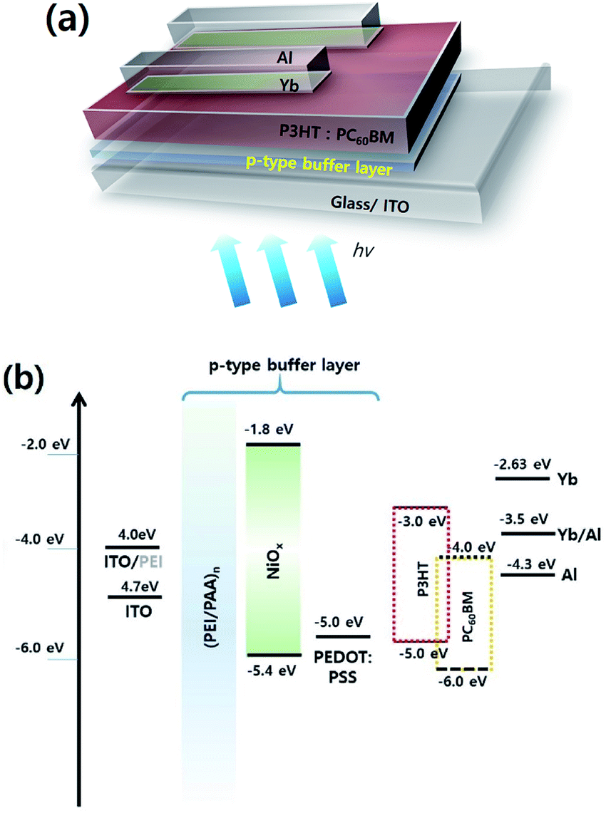 | ||
| Fig. 1 (a) Configuration of the prepared organic photodetector (OPD). (b) Energy diagrams of OPDs comprising three different p-type buffer layers. | ||
As shown in Fig. 1(b), the (PEI/PAA)n film has a wide bandgap (as an insulator), which imparts an excellent carrier-blocking capability but allows limited carrier transport.29–32 In very thin insulators (less than 3–4 nm), electrons tunnel directly through the trapezoidal potential barrier of the insulator, while in thick insulators, electrons tunnel through the triangular potential barrier under an external electric field (Fowler–Nordheim tunneling).33 The potential barrier formed by the energy level difference between the materials constituting the electronic device causes the accumulation of carriers at the interface, which results in band bending.34,35 In the device comprising the (PEI/PAA)n film, electron tunneling occurs because of interfacial energy band bending due to the accumulation of photogenerated holes between (PEI/PAA)n and the active layer under an external electric field; this is schematically illustrated in Fig. 2. The work function of ITO in contact with PEI (at zero bias (0 V) and dark state) is 4.0 eV (Fig. 2(a)).28 Under a reverse bias (−1 V) and dark state (Fig. 2(b)), electron tunneling under an external electric field does not occur due to an energy barrier created by the lowest unoccupied molecular orbital (LUMO) of P3HT (−3.0 eV) as well as the LUMO of (PEI/PAA)n (−1.1 eV). Under the reverse bias (−1 V) and light state (Fig. 2(c)), the photogenerated holes are accumulated between the (PEI/PAA)n film and the active layer; thus, interfacial energy band bending occurs in the downward direction at the (PEI/PAA)n/P3HT interface. As a result, the energy barrier that prevented electron tunneling is reduced and electrons are injected from the electrode into the active layer. The detailed mechanism of hole accumulation was determined by impedance analysis.
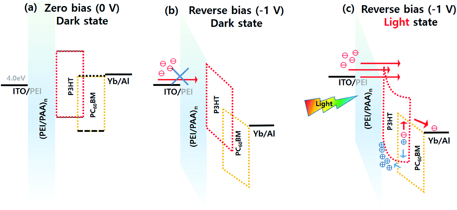 | ||
| Fig. 2 Light-assisted tunneling effect in the OPD comprising (PEI/PAA)n. (a) Zero bias (0 V) and dark state; (b) reverse bias (−1 V) and dark state; and (c) reverse bias (−1 V) and light state. | ||
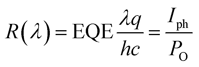
Responsivity and detectivity are important parameters in the evaluation of photodetectors. The responsivity (R(λ)) is the ratio between the generated photocurrent (Iph) and the amount of optical power (PO) incident on the detector, and is calculated from the EQE by the following equation:36
 | (1) |
 | (2) |
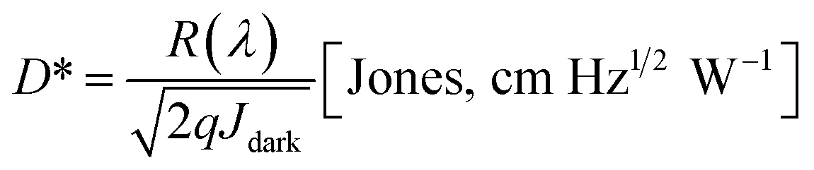
To achieve a high detectivity of the device comprising the (PEI/PAA)n films, we controlled the thickness of (PEI/PAA)n according to the number of bilayers (from 1 to 4). The thickness and roughness of the fabricated (PEI/PAA)1–4 films were measured by ellipsometry and atomic force microscopy (AFM), respectively, and the results are shown in Table S1 and Fig. S1.† The thicknesses of the (PEI/PAA)1, (PEI/PAA)2, (PEI/PAA)3, and (PEI/PAA)4 films are 3.3 ± 0.1, 7.4 ± 0.4, 12.2 ± 0.9, and 19.4 ± 0.2 nm, respectively. With the formation of 2 bilayers on a bare ITO, the root-mean-square (RMS) surface roughness greatly improved without a pinhole from 4.4 ± 0.3 nm (bare ITO) to 1.4 ± 0.2 nm (ITO/(PEI/PAA)2) in a 5 × 5 μm scan area. A similar roughness was observed above 2 bilayers. To achieve a statistically relevant result, we tested 30–32 nominally identical devices comprising different p-type buffer layers (Fig. S2†). As can be seen in Fig. S2(a),† the dark current (at −1 V) of the 2 bilayer is significantly lower than that of 1 bilayer and is similar for 2 bilayer to 4 bilayer samples. The photocurrent density (at 525 nm, 1 mW cm−2, and −1 V) decreased with an increase in the bilayer number (Fig. S2(b)†). Among the devices comprising the (PEI/PAA)1–4 films, the device using the (PEI/PAA)2 film shows the highest specific detectivity (3.11 × 10¹² Jones) at −1 V and 525 nm (Fig. S2(c)†). In the device using the (PEI/PAA)1 film, the (PEI/PAA)1 film was too thin to suppress the leakage current, whereas the (PEI/PAA)3–4 films in the respective devices were too thick to tunnel the electron.
We compared the performances of the developed device using (PEI/PAA)2 and the devices using general p-type buffer layers (PEDOT:PSS or NiOx), and the current density–voltage (J–V) characteristics are shown in Fig. 3. The J–V curve was measured in the dark and under illumination at λ = 525 nm (power density = 1 mW cm−2). The photocurrent density (Jph) of the device using (PEI/PAA)2 is 3.04 × 10⁻⁴ A cm−2 at −1 V, which is higher than that of the device using NiOx (2.89 × 10⁻⁴ A cm−2) but lower than that of the device using PEDOT:PSS (3.17 × 10⁻⁴ A cm−2). The photocurrent properties at 525 nm were calculated as the R according to eqn (1); the responsivities of the three devices using PEDOT:PSS, (PEI/PAA)2, and NiOx are 0.317, 0.304, and 0.289 A W−1, respectively. The Jdark of the device using (PEI/PAA)2 is 2.99 × 10⁻⁸ A cm−2 at −1 V, which is significantly lower than that of the device using PEDOT:PSS (1.40 × 10⁻⁵ A cm−2) and similar to that of the device using NiOx (2.94 × 10⁻⁸ A cm−2). Furthermore, D* was calculated using eqn (2). The device comprising (PEI/PAA)2 has the highest D* (3.11 × 10¹² Jones) at −1 V, while the D* values of the devices using NiOx and PEDOT:PSS were 2.98 × 10¹² and 1.50 × 10⁹ Jones, respectively. At a reverse bias larger than −1 V, the Jph of the device using (PEI/PAA)2 is higher than that of the device using PEDOT:PSS; however, the Jdark of the device using (PEI/PAA)2 increased, thereby decreasing the D* of the device using (PEI/PAA)2 from 3.11 × 10¹² (at −1 V) to 3.05 × 10¹² Jones (at −1.5 V).
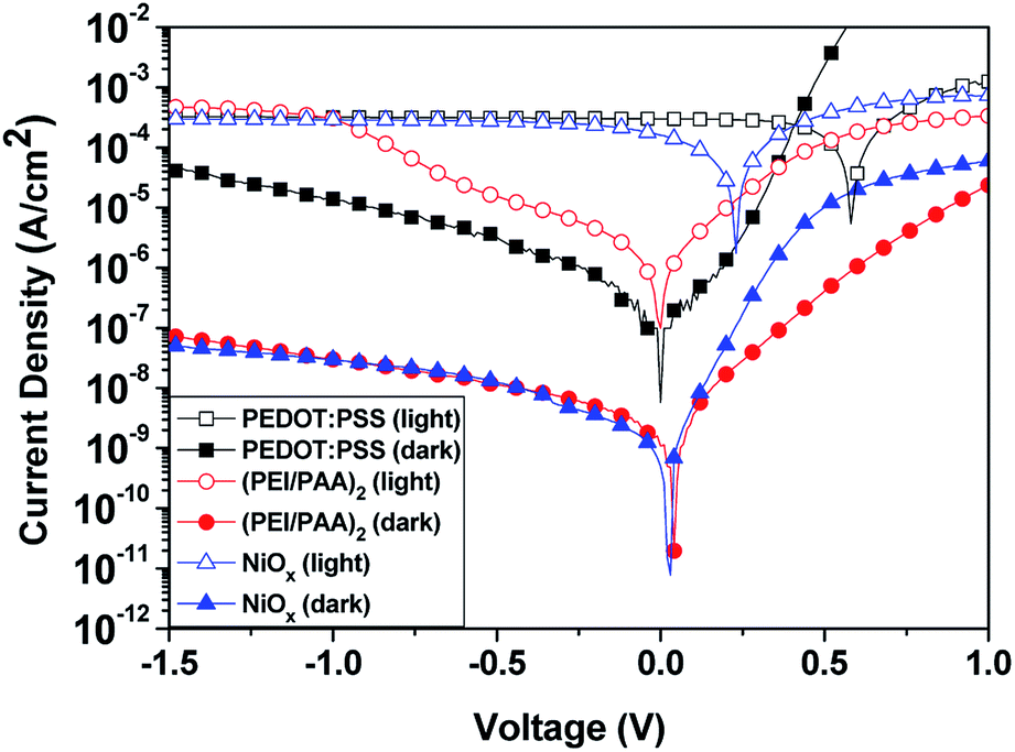 | ||
| Fig. 3 Logarithmic J–V characteristics of OPDs comprising different p-type buffer layers. | ||
The EQE and D* of the three devices using PEDOT:PSS, (PEI/PAA)2, and NiOx at different wavelengths are shown in Fig. 4. The devices show photoresponses from 300 to 650 nm. The broad spectral responsivities of these photodetectors (Fig. S3†) indicate their suitability for visible spectrum applications. The EQE and R are proportional to the intensity of light incident from the ITO side, which depends on the transmittance of the buffer layer inserted between the ITO and the active layer. As shown in Fig. S4,† the trends of EQE and responsivity agree well with the trend of transmittance, and (PEI/PAA)2 at 525 nm shows the same transmittance (90%) as that of PEDOT:PSS. From 350 to 600 nm, the D* of the device using (PEI/PAA)2 is more than 1 × 10¹² Jones, which is similar to or higher than that of the device using NiOx. In particular, at 350–450 nm, the D* of the device using (PEI/PAA)2 is significantly higher than that of the device using NiOx because (PEI/PAA)2 has a higher transmittance than NiOx. Moreover, the D* of the device using (PEI/PAA)2 is 10 times or more than that of the device using PEDOT:PSS. A comparison of these results with those of an organic-halide perovskite photodetector reported in the literature20,37 reveals that the device using (PEI/PAA)2 exhibits a similar detectivity (>1012 Jones at −1 V) in the visible-light region. In addition, the performance of the device with (PEI/PAA)2 achieved high D* and simultaneous suppression of the dark current compared to a similar reported device with a P3HT-based photodetector (Table S2†).12,49,51–53
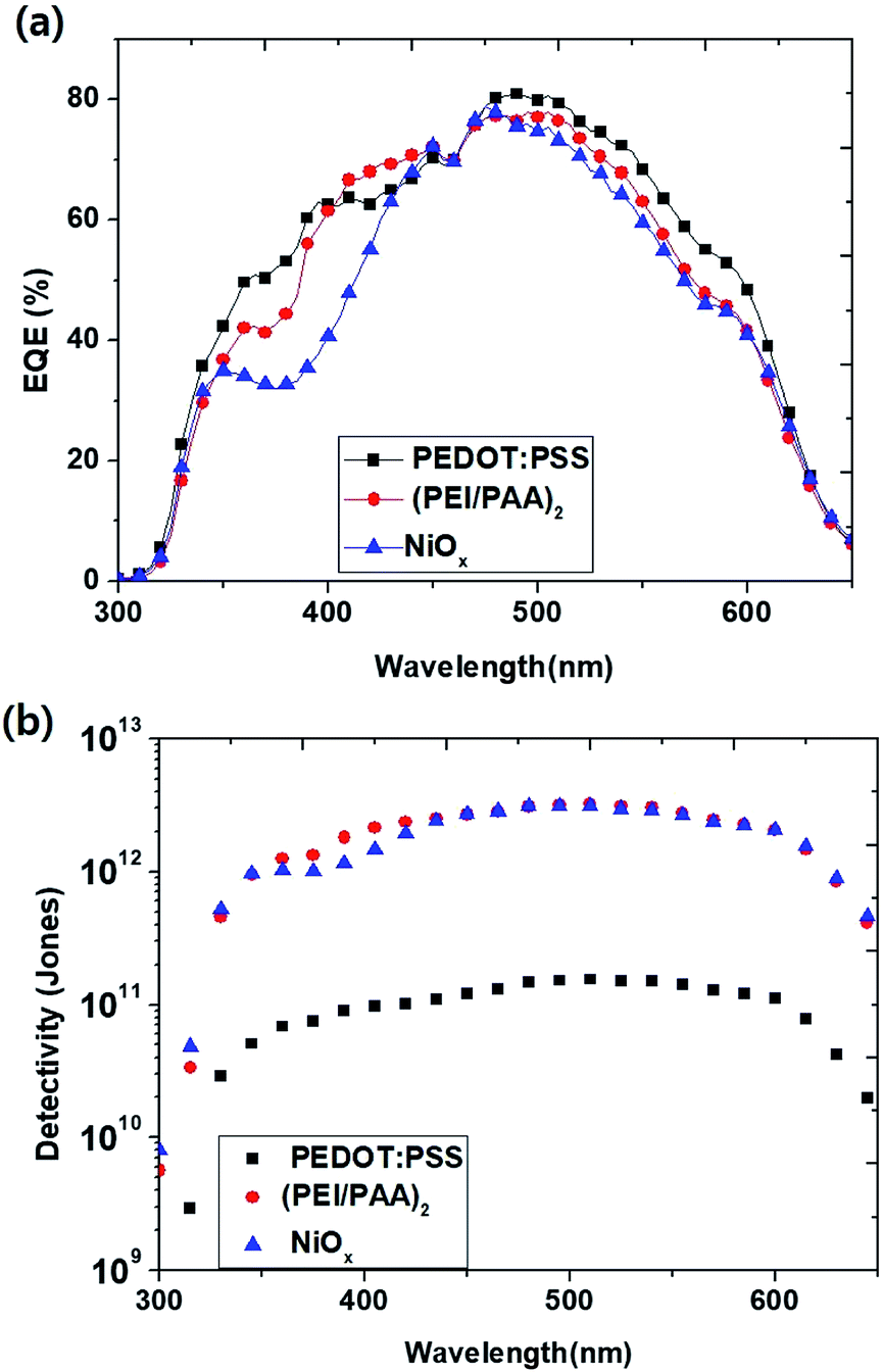 | ||
| Fig. 4 (a) External quantum efficiency (EQE) and (b) detectivity of OPDs at different wavelengths (−1 V and 1 mW cm−2). | ||
Another figure of merit for photodetectors is the linear dynamic range (LDR or photosensitivity linearity, typically expressed in dB), which is given as38
 | (3) |
 is the photocurrent measured at a light intensity of 1 mW cm−2. Fig. 5 shows the photocurrent density as a function of light intensity of the three devices comprising PEDOT:PSS, (PEI/PAA)2, and NiOx, respectively, at −1 V and 525 nm. The devices comprising (PEI/PAA)2 or NiOx show a linear response over the incident light intensity range from 10−3 to 102 mW cm−2 and have a LDR of 80.1 and 79.8 dB, respectively. This range is comparable to that of an organic-halide perovskite photodetector (>80 dB)20 and is higher than that of an InGaAs photodetector (66 dB).15 Thus, we confirmed that the device comprising (PEI/PAA)2 is suitable for the detection of a wide range of incident powers. However, the device comprising PEDOT:PSS shows a linear response over a narrower incident light intensity range from 3 × 10⁻¹ to 102 mW cm−2 and a low LDR of 27.1 dB. This implies that the photocurrent of the device comprising PEDOT:PSS cannot be distinguished by a high leakage current (or dark current) due to the low blocking ability of PEDOT:PSS under reverse bias (−1 V) at an incident light intensity of 10−1 mW cm−2 or less.
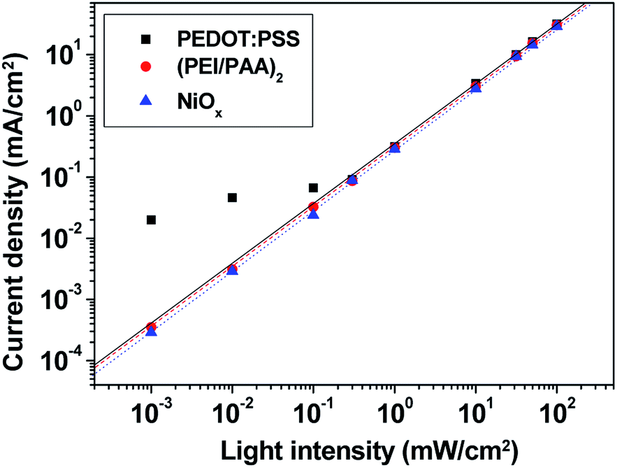 | ||
| Fig. 5 Photocurrent density as a function of light intensity (LDR) of OPDs at −1 V and 525 nm. | ||
To study the photogenerated hole accumulation at the (PEI/PAA)2/P3HT interface of the device, impedance measurements were carried out under light (525 nm, 1 mW cm−2) and dark conditions (100 Hz to 1 MHz) (Fig. 6). The device capacitance can be determined by the interfacial charge density in the OPD devices under illumination.39,40 Considering the device structure, the equivalent circuit shown in the inset of Fig. 6(a) was used as a model.41 From the fitted values of each element in the equivalent circuit model, the resistance and capacitance values were evaluated, which are listed in Table 1. R1 is the sheet resistance (20 Ω) through the ITO electrode, and R2 and C1 are the resistance and capacitance of the device excluding the ITO electrode, respectively. In Table 1, the C1 of the device using (PEI/PAA)2 irradiating light at −1 V is 2.90 nF, which is higher than that of the two devices using PEDOT:PSS (2.02 nF) or NiOx (2.32 nF), respectively. It can be argued that the holes generated by the light in P3HT:PC60BM are accumulated at the (PEI/PAA)2/P3HT interface by (PEI/PAA)2, which is a wide-bandgap insulator. Band bending occurs in the downward direction at the (PEI/PAA)2/P3HT interface due to the accumulated holes, as shown in Fig. 2, and electrons are tunneled from the electrode to the active layer under an external reverse bias. The C1 of the device using NiOx is slightly higher than that of the device using PEDOT:PSS because the holes transported from the active layer to the electrode are accumulated at the NiOx/P3HT interface due to the potential barrier created by NiOx having a deeper highest occupied molecular orbital (HOMO) (5.4 eV) than the HOMO of P3HT (5.0 eV).42,43 As a result, weak band bending occurs in the downward direction at the NiOx/P3HT interface and the holes are transferred from the HOMO of P3HT to the electrode through the HOMO of NiOx. This process is illustrated in Fig. S5.† In contrast, the device using PEDOT:PSS does not have a potential barrier at the PEDOT:PSS/P3HT interface due to the coincidence of the work function of PEDOT:PSS (5.0 eV) and the HOMO of P3HT (5.0 eV). Therefore, no charge accumulation occurs at the PEDOT:PSS/P3HT interface and thus, the C1 of the device using PEDOT:PSS is smaller than those of the other two devices. In the dark state at −1 V, the C1 of the device using (PEI/PAA)2 (0.47 nF) was similar to that of the device using NiOx (0.462 nF) and was significantly lower than that of the device using PEDOT:PSS (1.68 nF). This is because the blocking abilities of (PEI/PAA)2 and NiOx are superior to that of PEDOT:PSS, and the amount of residual (or trapped) charge inside the device decreased due to the blocking of carrier injection by an external reverse bias.
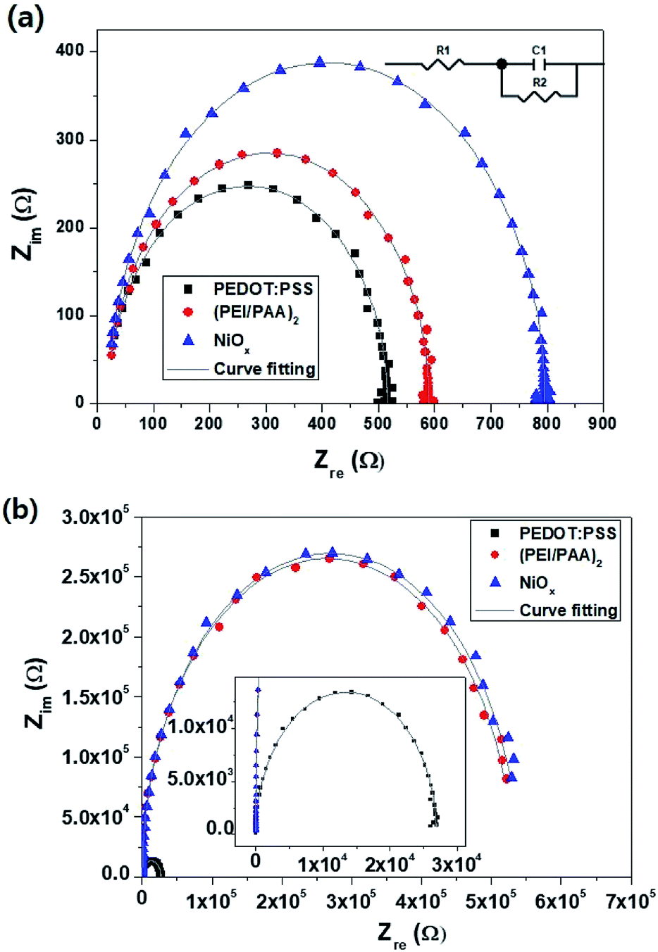 | ||
| Fig. 6 Impedance spectra measured under (a) light condition and (b) dark condition at 525 nm, −1 V and 1 mW cm−2. The inset in (a) shows the equivalent circuit used to model the impedance and the inset in (b) shows enlarged curves of the device comprising PEDOT:PSS. | ||
| PEDOT:PSS | (PEI/PAA)2 | NiOx | ||
|---|---|---|---|---|
| R1 (Ω) | 20 (ITO sheet resistance) | |||
| C1 (F) | Light | 2.02 × 10⁻⁹ | 2.90 × 10⁻⁹ | 2.32 × 10⁻⁹ |
| Dark | 1.68 × 10⁻⁹ | 4.70 × 10⁻¹⁰ | 4.62 × 10⁻¹⁰ | |
| R2 (Ω) | Light | 4.96 × 10² | 5.70 × 10² | 7.76 × 10² |
| Dark | 2.69 × 10⁴ | 5.31 × 10⁵ | 5.40 × 10⁵ | |
Impedance analysis can provide not only the capacitance component but also the resistance component of the device. As shown in Fig. 6(a) and Table 1, the R2 under light condition indicates the series resistance of the device and it changes depending on the active layer/electrode interfacial barrier (or resistance). The order of R2 of the three devices under light condition is NiOx (776 Ω) > (PEI/PAA)2 (570 Ω) > PEDOT:PSS (496 Ω). In terms of conductivity, which is the reciprocal of resistance, the above results are consistent with the photocurrent density trend of the three devices comprising different p-type buffer layers (Fig. 3). This implies that the series resistance, which inhibits the photocurrent (or charge transport) caused by the tunneling effect in the device using the (PEI/PAA)2 insulator, is comparable to that of the device using a general buffer layer (PEDOT:PSS or NiOx). Further, the R2 under dark condition indicates the shunt resistance of the device, which is related to its leakage current (Fig. 6(b) and Table 1). The R2 of the device using (PEI/PAA)2 (5.31 × 10⁵ Ω) under dark condition was similar to that of the device using NiOx (5.40 × 10⁵ Ω) and was significantly higher than that of the device using PEDOT:PSS (2.69 × 10⁴ Ω). This implies that the blocking abilities of (PEI/PAA)2 and NiOx inserted in the devices are superior to that of PEDOT:PSS, which effectively suppress the leakage current due to the external reverse bias, as shown by the J–V characteristics under dark conditions (Fig. 3). In addition, we analyzed the capacitance of the device using PEIE (single thin film, 7.5 nm) and (PEI/PAA)2 with similar thicknesses via impedance measurements (Fig. S6†). The capacitance of the device using (PEI/PAA)2 was higher than that of the device using PEIE (Table S3†). In addition, it was confirmed from the J–V characteristics that the device using PEIE had a lower photocurrent and a higher dark current than the device using (PEI/PAA)2 at −1 V (Fig. S7†). This is because the pinhole-free uniform thin film of (PEI/PAA)2 blocks the leakage currents and accumulates more charge, resulting in enhanced interfacial band bending.
The response speed of a photodetector is another important parameter for its evaluation. Some devices require the collection of optical signals over a certain bandwidth, such as a line scan camera (100 kHz) and optical communication (1 MHz),13–15 which requires rapid extraction of the photogenerated charge carriers. To demonstrate the speeds of our devices, we measured the rise times (tr) and decay times (td) of the photocurrent using an oscilloscope and a pulsed laser diode (525 nm, 1 mW cm−2). The rise and decay times are defined as the time taken for transition between 10% of the minimum current to 90% of the maximum current, and vice versa, respectively. Fig. 7(a) shows the transient photocurrent responses of the devices measured under −1 V at a pulse frequency of 20 kHz. The rise and decay times of the device using (PEI/PAA)2 were 4.5 and 6.7 μs, respectively, which are longer than those of the device using PEDOT:PSS (tr: 3.8 μs, td: 4.5 μs) but shorter than those of the device using NiOx (tr: 5.9 μs, td: 8.8 μs). Fig. 7(b) shows the normalized response vs. pulse frequency for the devices. The order of 3 dB bandwidth of the three devices at −1 V is PEDOT:PSS (140.1 kHz) > (PEI/PAA)2 (103.2 kHz) > NiOx (95.6 kHz). This clearly shows the difference in the response speeds of the three devices using different buffer layers and the difference in the response speed is related to the RC constant of the circuit.44 The impedance analysis results under light condition revealed that carrier accumulation in the devices using (PEI/PAA)2 is 1.25 times more than that in the device using NiOx; however, the resistance to charge transfer was 1.35 times lower. As a result, carrier extraction of the device using (PEI/PAA)2 was faster than that of the device using NiOx. Meanwhile, the interface resistance and charge accumulation of the device using PEDOT:PSS were significantly lower than those of the other two devices. Therefore, among the three devices, the device using PEDOT:PSS extracted the carriers the fastest. The device using (PEI/PAA)2 is faster than the reported quantum-dot photodetectors45,46 and its speed is comparable to that of the reported polymer detectors47,48 despite the time taken for charge accumulation and tunneling. Such a device is also applicable to industrial image processing such as line scan cameras.13
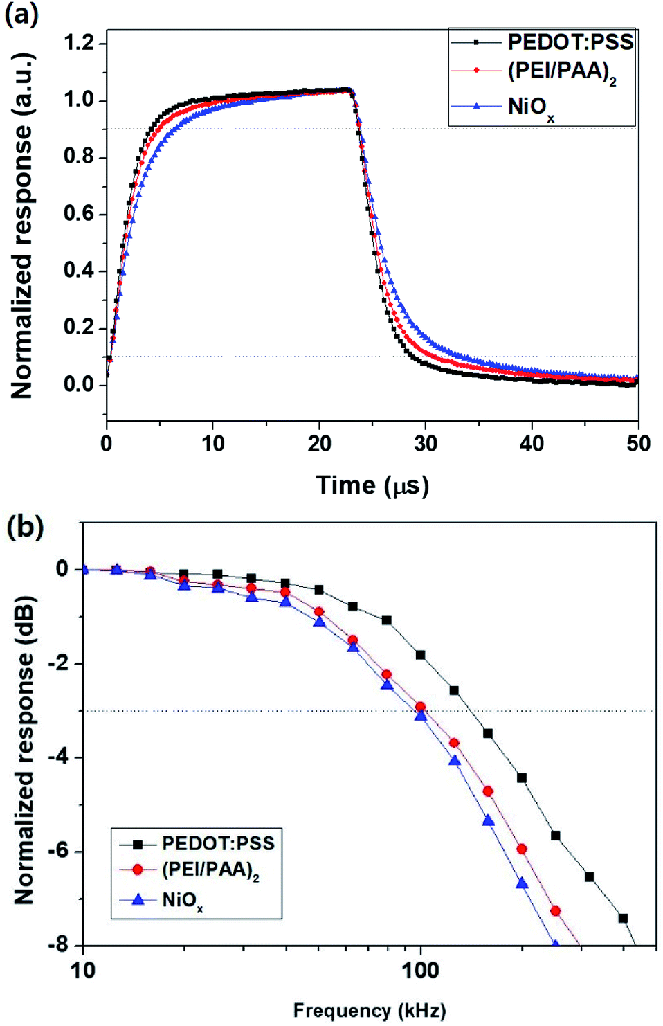 | ||
| Fig. 7 Transient photocurrent responses of the OPDs with different p-type buffer layers measured using a laser diode (1 mW cm−2, 525 nm) at −1 V. (a) Transient photocurrent responses of the OPDs at a pulse frequency of 20 kHz. (b) Frequency responses of the OPDs. | ||
Besides high detectivity and high response speed, long-term stability is also essential for the commercialization of OPDs. After fabrication, the stability of the devices was investigated in air at ambient temperature for over 168 h (7 days). To observe rapid changes, the devices were fabricated without encapsulation. As can be seen in Fig. 8, the device using (PEI/PAA)2 shows stable detectivity equivalent to that of the device using NiOx. After 168 h, the devices using (PEI/PAA)2 or NiOx retained a D* of > 1012 Jones (at 525 nm, −1 V), while that of the device using PEDOT:PSS decreased from 1.50 × 10¹¹ to 1.91 × 10¹⁰ Jones under the same conditions. The R and Jdark values of the devices used for the calculation of D* values are shown in Fig. S8.† In the device using PEDOT:PSS, the acidic PEDOT:PSS etches the ITO, thus deteriorating the device performance rapidly. In contrast, the device using (PEI/PAA)2 shows enough stability and detectivity to replace the NiOx by contacting the basic PEI with the ITO. On the other hand, in addition to atmospheric stability, the device showed thermal stability under continuous illumination, which is an important behavior. The device using (PEI/PAA)2 was found to have dark current and photocurrent similar to the initial level after exposure to 1 sun for 4 h (Fig. S9†).
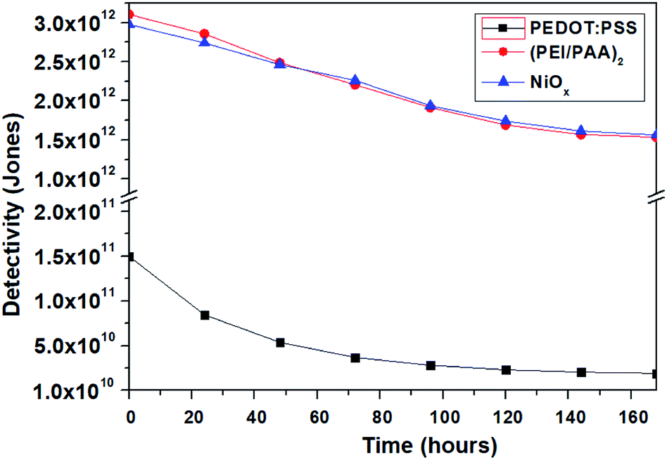 | ||
| Fig. 8 Detectivity of the OPDs over 168 h (7 days) after fabrication in air under 525 nm (1 mW cm−2) illumination (at −1 V). | ||
Conclusions
We demonstrated the behavior of (PEI/PAA)2 fabricated by a spin-assisted LBL technique as a p-type buffer layer of a P3HT-based OPD. At −1 V and 525 nm, the detectivity of the device using (PEI/PAA)2 (3.11 × 10¹² Jones) was higher than that of the devices using NiOx or PEDOT:PSS due to the light-assisted tunneling effect, even though an insulator (PEI/PAA multilayers) was used as a p-type buffer layer. In the device using (PEI/PAA)2, the light-assisted tunneling effect occurred at a low light intensity of 1 × 10⁻³ mW cm−2 and the device exhibited a LDR of 80.1 dB, which is higher than that of an InGaAs photodetector (66 dB). In addition, the device using (PEI/PAA)2 has a bandwidth of more than 100 kHz and is applicable to the industrial image processing field such as line scan cameras. Moreover, our results indicate that it is possible to replace metal oxide buffer layers (e.g., NiOx), which require high-temperature processing, and to apply flexible, large-area substrates because the device using (PEI/PAA)2 is fabricated by a low-temperature solution process.Conflicts of interest
There are no conflicts to declare.Acknowledgements
This research was supported by Basic Science Research Program through the National Research Foundation of Korea (NRF) funded by the Ministry of Education (NRF-2017R1D1A1B03028795). This study was supported by “Human Resources Program in Energy Technology” of the Korea Institute of Energy Technology Evaluation and Planning (KETEP), granted financial resource from the Ministry of Trade, Industry and Energy, Republic of Korea (No. 20174010201150).References
- D. Yang and D. Ma, Adv. Opt. Mater., 2019, 7, 1800522 CrossRef.
- F. Teng, K. Hu, W. Ouyang and X. S. Fang, Adv. Mater., 2018, 30, 1706262 CrossRef PubMed.
- R. D. J. Vuuren, A. Armin, A. K. Pandey, P. L. Burn and P. Meredith, Adv. Mater., 2016, 28, 4766 CrossRef PubMed.
- F. P. García de Arquer, A. Armin, P. Meredith and E. H. Sargent, Nat. Rev. Mater., 2017, 2, 16100 CrossRef.
- Y. Dong, Y. Zou, J. Song, J. Li, B. Han, Q. Shan, L. Xu, J. Xue and H. Zeng, Nanoscale, 2017, 9, 8580 RSC.
- R. Eckstein, T. Rödlmeier, T. Glaser, S. Valouch, R. Mauer, U. Lemmer and G. Hernandez Sosa, Adv. Electron. Mater., 2015, 1, 1500101 CrossRef.
- S. Xiong, J. Tong, L. Mao, Z. Li, F. Qin, F. Jiang, W. Meng, T. Liu, W. Li and Y. Zhou, J. Mater. Chem. C, 2016, 4, 1414 RSC.
- A. Pierre, I. Deckman, P. B. Lechene and A. C. Arias, Adv. Mater., 2015, 27, 6411 CrossRef CAS PubMed.
- J. Qi, J. Han, X. Zhou, D. Yang, J. Zhang, W. Qiao, D. Ma and Z. Y. Wang, Macromolecules, 2015, 48, 3941 CrossRef CAS.
- H. Arora, P. E. Malinowski, A. Chasin, D. Cheyns, S. Steudel, S. Schols and P. Heremans, Appl. Phys. Lett., 2015, 106, 143301 CrossRef.
- G. Pace, A. Grimoldi, D. Natali, M. Sampietro, J. E. Coughlin, G. C. Bazan and M. Caironi, Adv. Mater., 2014, 26, 6773 CrossRef CAS PubMed.
- B. Arredondo, B. Romero, J. M. S. Pena, A. Fernández-Pacheco, E. Alonso, R. Vergaz and C. de Sios, Sensors, 2013, 13, 12266 CrossRef PubMed.
- D. Baierl, L. Pancheri, M. Schmidt, D. Stoppa, G.-F. Dalla Betta, G. Scarpa and P. Lugli, Nat. Commun., 2012, 3, 1175 CrossRef PubMed.
- C. H. Ji, K. T. Kim and S. Y. Oh, RSC Adv., 2018, 8, 8302 RSC.
- L. Dou, Y. Yang, J. You, Z. Hong, W.-H. Chang, G. Li and Y. Yang, Nat. Commun., 2014, 5, 5404 CrossRef CAS PubMed.
- S. B. Lim, C. H. Ji, I. S. Oh and S. Y. Oh, J. Mater. Chem. C, 2016, 4, 4920 RSC.
- M. Ramuz, L. Bürgi, C. Winnewisser and P. Seitz, Org. Electron., 2008, 9, 369 CrossRef CAS.
- I. J. Park, M. A. Park, D. H. Kim, G. D. Park, B. J. Kim, H. J. Son, M. J. Ko, D.-K. Lee, T. Park, H. Shin, N.-G. Park, H. S. Jung and J. Y. Kim, J. Phys. Chem. C, 2015, 119, 27285 CrossRef CAS.
- H. Si, Q. Liao, Z. Zhang, Y. Li, X. Yang, G. Zhang, Z. Kang and Y. Zhang, Nano Energy, 2016, 22, 223 CrossRef CAS.
- B. R. Sutherland, A. K. Johnston, A. H. Ip, J. Xu, V. Adinolfi, P. Kanjanaboos and E. H. Sargent, ACS Photonics, 2015, 2, 1117 CrossRef CAS.
- W. Ma, H. Xu and A. Takahara, Adv. Mater. Interfaces, 2014, 1, 1300092 CrossRef.
- W. Yuan, Z. Lu and C. M. Li, J. Mater. Chem., 2012, 22, 9351 RSC.
- Y. H. Yang, M. Haile, Y. T. Park, F. A. Malek and J. C. Grunlan, Macromolecules, 2011, 44, 1450 CrossRef CAS.
- J. T. Stricker, A. D. Gudmundsdóttir, A. P. Smith, B. E. Taylor and M. F. Durstock, J. Phys. Chem. B, 2007, 111, 6322 CrossRef CAS PubMed.
- P. G. Ganesan, J. Gamba, A. Ellis, R. S. Kane and G. Ramanath, Appl. Phys. Lett., 2003, 83, 3302 CrossRef CAS.
- M. Alba-Martin, T. Firmager, J. Atherton, M. C. Rosamond, D. Ashall, A. Al Ghaferi, A. Ayesh, A. J. Gallant, M. F. Mabrook, M. C. Petty and D. A. Zeze, J. Phys. D: Appl. Phys., 2012, 45, 295401 CrossRef.
- C. -C. Chueh, C. -Z. Li and A. K. Y. Jen, Energy Environ. Sci., 2015, 8, 1160 RSC.
- H. Kang, S. Hong, J. Lee and K. Lee, Adv. Mater., 2012, 24, 3005 CrossRef CAS PubMed.
- H. B. Kim, Y. J. Yoon, J. Jeong, J. Heo, H. Jang, J. H. Seo, B. Walker and J. Y. Kim, Energy Environ. Sci., 2017, 10, 1950 RSC.
- Y. Zhu, A. Apostoluk, P. Gautier, A. Valette, L. Omar, T. Cornier, J. M. Bluet, K. Masenelli-Varlot, S. Daniele and B. Maseneli, Sci. Rep., 2016, 6, 23557 CrossRef CAS PubMed.
- Z. Lin, J. Chang, J. Zhang, C. Jiang, J. Wu and C. Zhu, J. Mater. Chem. A, 2014, 2, 7788 RSC.
- L. Y. Cui, R. C. Zeng, S. Q. Li, F. Zhang and E. H. Han, RSC Adv., 2016, 6, 63107 RSC.
- K. Roy, S. Mukhopadhyay and H. Mahmoodi-Meimand, Proc. IEEE, 2003, 91, 305 CrossRef CAS.
- C. V. Hoven, R. Yang, A. Garcia, V. Crockett, A. J. Heeger, G. C. Bazan and T.-Q. Nguyen, Proc. Natl. Acad. Sci. U. S. A., 2008, 105, 12730 CrossRef CAS PubMed.
- Y. F. Chen, Y. T. Tsai, D. M. Bassani, R. Clerc, D. Forgacs, H. J. Bolink, M. Wussler, W. Jaegermann, G. Wantz and L. Hirsch, J. Mater. Chem. A, 2016, 4, 17529 RSC.
- Y. Fang, F. Guo, Z. Xiao and J. Huang, Adv. Opt. Mater., 2014, 2, 348 CrossRef CAS.
- Q. Lin, A. Armin, D. M. Lyons, P. L. Burn and P. Meredith, Adv. Mater., 2015, 27, 2060 CrossRef CAS PubMed.
- X. Gong, M. Tong, Y. Xia, W. Cai, J. S. Moon, Y. Cao, G. Yu, C. L. Shieh, B. Nilsson and A. J. Heeger, Science, 2009, 325, 1665 CrossRef CAS PubMed.
- B. Chen, X. Qiao, C.-M. Liu, C. Zhao, H.-C. Chen, K.-H. Wei and B. Hu, Appl. Phys. Lett., 2013, 102, 193302 CrossRef.
- S. Cho, K. D. Kim, J. Heo, J. Y. Lee, G. Cha, B. Y. Seo, Y. D. Kim, Y. S. Kim, S. Y. Choi and D. C. Lim, Sci. Rep., 2014, 4, 4306 CrossRef PubMed.
- K. H. Lee, G. H. Lee, D. S. Leem, J. Lee, J. W. Chung, X. Bulliard, H. Choi, K.-B. Park, K.-S. Kim, Y. W. Jin, W. Lee and S. Y. Park, J. Phys. Chem. C, 2014, 118, 13424 CrossRef CAS.
- A. Singh, S. K. Gupta and A. Garg, Sci. Rep., 2017, 7, 1775 CrossRef PubMed.
- J. Kim, Y. Ko and K. Park, Acta Phys. Pol., A, 2018, 133, 887 CrossRef CAS.
- Y. Yao, Y. Liang, V. Shrotriya, S. Xiao, L. Yu and Y. Yang, Adv. Mater., 2007, 19, 3979 CrossRef CAS.
- J. P. Clifford, G. Konstantatos, K. W. Johnston, S. Hoogland, L. Levina and E. H. Sargent, Nat. Nanotechnol., 2009, 4, 40 CrossRef CAS PubMed.
- V. Adinolfi, I. J. Kramer, A. J. Labelle, B. R. Sutherland, S. Hoogland and E. H. Sargent, ACS Nano, 2015, 9, 356 CrossRef CAS PubMed.
- A. Armin, R. D. Jansen-van Vuuren, N. Kopidakis, P. L. Burn and P. Meredith, Nat. Commun., 2015, 6, 6343 CrossRef CAS PubMed.
- S. F. Tedde, J. Kern, T. Sterzl, J. Furst, P. Lugli and O. Hayden, Nano Lett., 2009, 9, 980 CrossRef CAS PubMed.
- Y. Wang, L. Zhu, Y. Hu, Z. Deng, Z. Lou, Y. Hou and F. Teng, Opt. Express, 2017, 25, 7719 CrossRef CAS PubMed.
- M. H. Yoon, A. Facchetti and T. J. Marks, Proc. Natl. Acad. Sci. U. S. A., 2015, 102, 4678 CrossRef PubMed.
- R. Dong, C. Bi, Q. Dong, F. Guo, Y. Yuan, Y. Fang and J. Huang, Adv. Opt. Mater., 2014, 2, 549 CrossRef CAS.
- G. Azzellino, A. Grimoldi, M. Binda, M. Caironi, D. Natali and M. Sampietro, Adv. Mater., 2013, 25, 6829 CrossRef CAS PubMed.
- A. Grimoldi, L. Colella, L. L. Monaca, G. Azzellino, M. Caironi, C. Bertarelli, D. Natali and M. Sampietro, Org. Electron., 2016, 36, 29 CrossRef CAS.
Footnote |
| † Electronic supplementary information (ESI) available: Thickness and surface roughness of bilayers; AFM images of bilayers on ITO substrates; device statistics for dark current density, photocurrent density, and detectivity of OPDs; responsivities of OPDs; transmittances of p-type buffer layers; carrier transport mechanism of the device using NiOx; dark current densities and responsivities of OPDs. See DOI: 10.1039/c9ra08568h |
| This journal is © The Royal Society of Chemistry 2019 |