
 Open Access Article
 This Open Access Article is licensed under a Creative Commons Attribution-Non Commercial 3.0 Unported Licence
Optical characteristics of GaAs/GaAsSb/GaAs coaxial single quantum-well nanowires with different Sb components
Haolin Lia,
Jilong Tang a,
Guotao Pangb,
Dengkui Wanga,
Xuan Fanga,
Rui Chen*b and
Zhipeng Wei*a
a,
Guotao Pangb,
Dengkui Wanga,
Xuan Fanga,
Rui Chen*b and
Zhipeng Wei*a
aState Key Laboratory of High Power Semiconductor Laser, School of Science, Changchun University of Science and Technology, Changchun 130022, P. R. China. E-mail: zpweicust@126.com
bDepartment of Electrical and Electronic Engineering, Southern University of Science and Technology, Shenzhen, Guangdong 518055, P. R. China. E-mail: chenr@sustech.edu.cn
First published on 21st November 2019
Abstract
III–V ternary alloy quantum-wells have become a hot topic in recent years. Especially, GaAs/GaAsSb quantum wells have attracted increasing attention due to their numerous applications in the field of near-infrared optoelectronic devices. With the further reduction of dimensions, GaAs/GaAsSb nanowires show many special properties compared to their quantum well structures. In this work, GaAs/GaAs1−xSbx/GaAs coaxial single quantum-well nanowires with different Sb composition were grown by molecular beam epitaxy. The band structure and the optical properties were investigated through power-dependent and temperature-dependent photoluminescence measurement. It has been found that a deeper quantum well is created with the increase of Sb component. Thanks to the deeper quantum well, more effective electron confinement has been realized, the emission from the sample can still be detected up to room temperature. The different trend of peak position and shape at various temperatures also supports the improved temperature stability of the samples. These results will be beneficial for the design of alloy quantum wells, and will facilitate the development of alloy quantum-well based devices.
Introduction
III–V ternary alloys have attracted ever increasing attention because of the promises offered by their bandgaps for specific optoelectronic applications.1–3 As one of the most important narrow-band ternary alloys, GaAsSb has large bandgap tunability which can be modulated between 1.42 eV (GaAs) and 0.73 eV (GaSb), by adjusting the Sb concentration.4 The tailored materials can be used in numerous applications such as lasers,5–8 infrared photodetectors,9,10 and solar cells.11,12 More importantly, the bandgap of GaAs/GaAsSb quantum-wells can reach the optical communication window,3,7 which has attracted widespread attention in the study of GaAs/GaAsSb quantum-well structures. With the development of information technology, the demand for nanoscale devices is becoming more intensive. Semiconductor nanowires offer new routes toward nanoscale optoelectronic devices that can be a natural one-dimensional optical waveguide and be site-selectively integrated onto silicon photonic circuits. When the dimension reduces, the quantum confinement effect will be more pronounced. Therefore, it is necessary to study the optical property of quantum well nanowires.Until now, GaAsSb nanowires with various compositions can be grown by tuning the ratio between Sb and As fluxes,4 and a single-mode lasing in a GaAsSb-based nanowire superlattice has been realized at room-temperature.5 The heterostructured nanowires are important for both physical understanding and technological application. However, up till now, the growth of GaAsSb/GaAs heterostructures with type-I or type-II band alignment has been controversially discussed for many years for different types of nanostructures. In our previous study,13 we have investigated the optical properties of GaAs/GaAsSb/GaAs coaxial single quantum-well nanowires. It is found the compositional change of Sb has a great influence on the quantum well structure. GaAs/GaAsSb/GaAs quantum well with Sb composition about 8% cannot effectively confine electrons, which leads to a poor thermal stability.
In this work, nanowire quantum well structure with improved optical properties was proposed and fabricated and the photoluminescence from GaAs/GaAsSb/GaAs coaxial single quantum-well nanowires with different Sb components was discussed. As the Sb composition increase, GaAs/GaAs0.88Sb0.12/GaAs quantum well nanowires exhibit more effective electron confinement due to the larger conduction band offset. During the photoluminescence (PL) characterization, a larger blue shift of emission peak occurs with increasing excitation power at low temperature. The observation proves that a deeper quantum well is created with the increase of Sb component. During the temperature-dependent PL measurement, it is noted that the emission from the sample can still be detected up to room temperature. The improved temperature stability of the sample has also been discussed in terms of the peak position and peak shape at various temperatures. Those results show the importance of the design of nanowires alloy for quantum-wells, which will facilitate the development of alloy quantum-well based nanoscale devices.
Experimental
The GaAs/GaAsSb/GaAs coaxial single quantum-well nanowires used herein were fabricated on Si substrate using a DCA P600 solid source molecular beam epitaxy (MBE) system. Specific growth parameters can be referred to our previous publication.13,14 The Sb component in the GaAs1−xSbx layer can be well-controlled by adjusting the beam ratio of the As and Sb fluxs. For sample A, the beam equivalent pressure of As was set to 2.1 la10−6 torr and the Sb flux was set to 1.9 s 10−7 torr. For sample B, the beam equivalent pressure of As reduced to 2.0 × 10⁻⁶ torr, while Sb flux increased to 2.8 × 10⁻⁷ torr. During the material growth, the other growth conditions are the same as the previous report.13 The detail growth process of pure GaAs nanowires is the same as the growth of GaAs cores in GaAs/GaAsSb/GaAs coaxial single quantum-wells nanowires.Scanning electron microscopy (SEM, Hitachi S-4800) and energy-dispersive X-ray spectroscopy (EDX, EDAX mounted on a FEI Talos F200X high-angle annular dark field scanning transmission electron microscopy (STEM) system) were used to characterize the morphological properties of the samples. For optical property characterization, a 655 nm semiconductor diode laser was used as the excitation source with a laser spot size of about 0.4 cm2. The emission is dispersed by HORIBA iHR550 monochromator, and the PL signal was detected by a Peltier cooled InGaAs photodiode. Standard phase lock-in amplifier technique was employed to improve the signal-to-noise ratio. The excitation power of the laser was fixed at 100 mW during the temperature-dependent PL measurement, and the temperature can be well-controlled within a closed-cycle helium cryostat. During the power-dependent PL measurement, the temperature of the sample was fixed at 10 K.
Results and discussion
In our previous work,13 GaAs/GaAs0.92Sb0.08/GaAs coaxial single quantum-well nanowires (sample A) has been reported. When the Sb concentration is 8%, there is a quasi-type-II band structure and the conduction band offset between GaAs and GaAsSb is about 20 meV, which is not large enough to confine electrons. As the researchers pointed out,15 the GaAs/GaAs1−xSbx band alignment has a type-I to type-II crossover at a Sb mole fraction of x = 0.4. The maximum value of conduction offset appears at about x = 0.2. In order to improve the optical properties of quantum well nanowires, GaAs/GaAs0.88Sb0.12/GaAs coaxial single quantum-well nanowires (sample B) has been grown. In GaAs/GaAs0.88Sb0.12 quantum-well, quasi-type-II band structure still exists, but the conduction band offset between GaAs and GaAsSb increases. Theoretically, the quantum well in sample B is more restrictive to electrons than sample A.Fig. 1(a) and (b) show the SEM image taken from a similar position on the wafers of sample A and sample B, respectively. Both samples demonstrate straight nanowires grown on Si substrates with comparable diameters of ∼200 to 230 nm and length of ∼5 to 7 μm. The GaAs core is about 160–180 nm, and the thickness of GaAsSb quantum well and GaAs cap are about 10 nm. The description of the STEM and selective area electron diffraction (SAED) of sample B is shown in Fig. 1(c) and (d), respectively. From the STEM and SAED pattern, the structure of GaAs is mainly ZB (zinc blende) structure. To evaluate the material composition, EDX analysis was used. As shown in Fig. 1(e), there is a slight inhomogeneity of Sb distribution and the average atomic percentage of the Sb in sample B is about 6%. The EDX data presents the percentage of each atom in total atoms. It can be seen that both Ga and As atoms are about 50%. Therefore, 6% of Sb in the figure actually means that the atomic ratio of As vs. and Sb is 88% vs. and 12%, respectively. The 12% Sb composition in sample B is slightly larger than 8% Sb composition in sample A (the EDX and STEM image of sample A can be found in our previous publication13). The PL spectrum of the two samples at low temperature (10 K) is shown in Fig. 1(f). The peak position of sample A was at 1.35 eV and the peak position of sample B was at 1.31 eV. The peak energy of both samples was smaller than GaAs nanowires (1.515 eV at 10 K), indicating that the luminescence comes from the GaAs/GaAsSb quantum-well. In addition, the full width at half maximum (FWHM) of sample A was ∼68.8 meV and sample B was ∼63.7 meV. A similar FWHM indicates the high growth quality of the two samples. Since the large conduction band offset, electrons in sample B need more energy to overcome the barrier. Therefore, the type-II like emission (at larger energy side) in sample B is not as pronounced as in sample A.
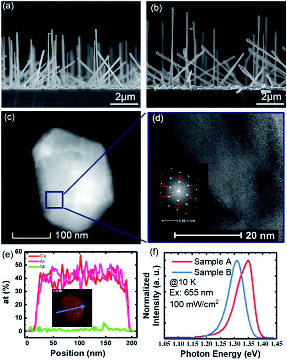 | ||
| Fig. 1 GaAs/GaAsSb/GaAs coaxial single quantum-well nanowires with different Sb component. (a) and (b) SEM image of sample A and sample B, separately. (c) STEM image of sample B. (d) STEM image taken from the GaAs core, the inset is typical SAED patterns. (e) EDX spectrum of the cross section from sample B. (f) Low temperature PL emission. | ||
The power-dependent PL spectra at low-temperature (10 K) of sample A and sample B are depicted in Fig. 2(a) and (b), respectively. As can be seen from the figure, the peak position of both samples shows a blue shift with the increase of excitation power, which is totally different from the pure GaAs nanowires. Laser thermal effect may lead to the shifting of emission, but generally a red shift rather than the blue shift. In this work, the blue shift can be ascribed to the shallow quantum-well. When the excitation power increased, more photogenerated carriers are generated, the band filling effect and the change in the proportion of emission sources cause the blue shift of the peak position. In quasi-type-II band alignment, there are two recombination channels for excitons at the same time, one is the recombination between the photoexcited electrons and holes are localized in the well material (type-I like recombination), and the other is the recombination between the photoexcited electron and hole are localized in two different semiconductors (type-II like recombination). The band structure of GaAs1−xSbx in the quantum well can be described by the empirical model proposed by Teissier et al.13,16 As it is shown in Fig. 2(d), the conduction bandgap offset in sample A and sample B is ∼20 meV and ∼28 meV, respectively. There may be a mixed structure of WZ (wurtzite) and ZB in the GaAs core.17 However, the conduction band edge of the WZ GaAs is far away from the GaAsSb conduction band, therefore, the existence of a small amount of WZ structure does not affect the quasi-type-II band arrangement. It is true that during the measurement, no emission from the WZ GaAs and the recombination between WZ GaAs and GaAsSb have been observed. With the increase of excitation power, more elections obtain enough thermal energy through collisions. They will overcome the barrier and diffuse to the GaAs conduction band, which contributed to the type-II like recombination. Due to the large conduction band offset, the energy offset between type-I and type-II of sample B is larger than that of sample A, and the blue shift in sample B is larger than sample A, as Fig. 2(c) presents. The smaller slope also attributed to the smaller conduction band offset in sample A. With the smaller barrier, the transition of the electrons between the well layer and the barrier layer becomes easy at the beginning, and the influence of proportional change induced by the power increase becomes weak. The smaller blue shift compared with the band offset is due to the quantum confinement effect and the contribution of the two emissions change.
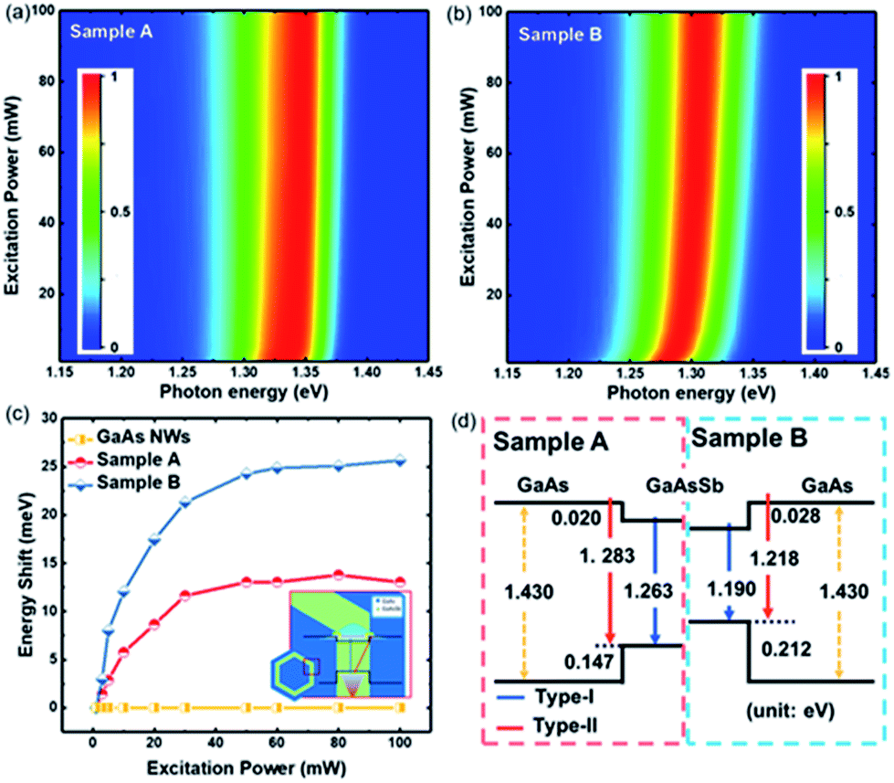 | ||
| Fig. 2 Low temperature PL under different excitation intensities. (a) Sample A. (b) Sample B. (c) Energy shift with excitation power. (d) Schematic band structure (the scale bar in (a) and (b) represents the normalized emission intensity). | ||
Temperature-dependent PL measurement performed between 10 and 300 K is a further evidence of the band structures of the two samples more effective electron confinement in sample B larger than sample A is witnessed by temperature-dependent PL measurement performed between 10 and 300 K. Surrounding environments is another energy source from which carriers can get. With the increase of temperature, electrons confined in quantum-well can obtain enough thermal energy to overcome the energy barrier and diffuse to GaAs. Due to the spatial separation of electrons and holes, the luminescence efficiency of type-II band structure has an inefficient recombination rate. With electrons diffuse to GaAs layer, the intensity of emission will decrease. In order to clearly show the trend of the peak position and FWHM with temperature, the emission spectrum is normalized and vertically shifted in y-direction for easier comparison, as shown in Fig. 3. The PL emission of sample B can be found for the whole temperature range. In contrast, when the temperature increases up to 240 K, the PL emission of sample A disappear. The peak evolution of the two samples with temperature also shows different trends.
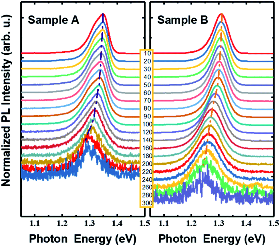 | ||
| Fig. 3 Normalized PL emission with temperature dependent. | ||
The peak position change with temperature of two samples has been plotted in Fig. 4(a), respectably. Cubic yellow one is from pure GaAs nanowires, which can be well fitted by Varshni equation:18
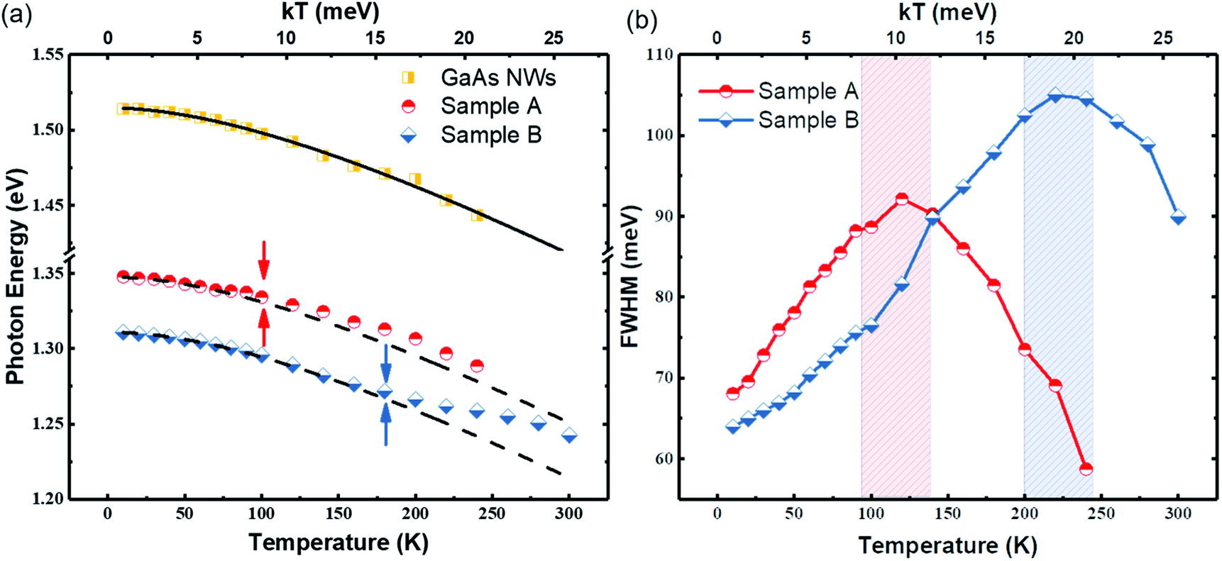 | ||
| Fig. 4 (a) Photon energy shift with temperature (the solid line is the fitting result according to the Varshni equation. The dash lines were obtained by shifting the solid line vertically). (b) FWHM change with temperature (the shadow is used to indicate the inflection point). | ||
The existence of the inflection point can be explained by the GaAs/GaAsSb quantum-well structure. As has been pointed out above, once electrons confined in quantum-well obtain enough thermal energy from the surrounding environment, they will have a greater chance to overcome the barrier and diffuse to the barrier. The type-II like emission has a large photon energy, which leads to a blue shift of the emission. The difference in emission evolution is caused by different ratios of carriers' pathways. For sample A, the inflection point located at ∼100 K (∼8 meV). The inflection point of sample B located at ∼180 K (∼16 meV), which is larger than sample A. By calculation, we obtained a conduction band offset of about 20 meV in sample A and 28 meV in sample B, as it is shown in Fig. 2(d). Considering the effective ground state energy level in one-dimensional square well, the ground state energy in quantum is slightly higher than the GaAsSb conduction band minimum. By solving the one-dimensional time-invariant Schrödinger equation, we obtain the ground state energy levels of electrons in a finite deep quantum well. Electrons in sample A require 8 meV to jump out of the well, and about 14 meV in sample B, which corresponds to the inflection point.
The FWHM of the whole peak was calculated from Fig. 3 and the result is shown in Fig. 4 as a function of temperature. The FWHM as a function of temperature also has two parts. In the low temperature range, the FWHM of the two samples is almost linearly broadened as the temperature increases. With the increase of temperature above the inflection point, a narrowed FWHM can be observed. The temperature induced FWHM broadening is related to the carrier distribution. However, the narrowing behaviour is impossible to reconcile with a model involving only a single inhomogeneously broadened transition. It is natural to related the narrowing of FWHM to the disappearance of a recombination mechanism.21–23 In this model the narrowing of the FWHM is also due to the shallow well. When electrons obtain enough thermal energy will diffuse to the barrier, the emission from type-I will decrease until disappearing. Similar phenomenon has also been found the quantum structure of other material, such as InGaN/GaN multiple quantum wells.24 The maximum FWHM for sample B is larger than sample A, which further supports the deeper quantum-well in sample B.
Conclusions
In summary, nanowire quantum well structure with improved optical properties was designed and fabricated. During the laser spectroscopy characterization, the larger blue shift of emission peak has been observed with increasing excitation power at low temperature, which proves the deeper quantum well with the increase of Sb component. Thanks to the deeper quantum well, emission from GaAs/GaAs0.88Sb0.12/GaAs quantum well nanowires can suffer higher temperature. The peak position and shape of quantum well at various temperatures show different trends compared to pure GaAs nanowires. The temperature stability of the sample has also been improved through the effective electron confinement due to the larger conduction band offset. Those results show the importance of the design of nanowires alloy quantum-wells, which will facilitate the development of alloy quantum-well based nanoscale devices.Conflicts of interest
There are no conflicts to declare.Acknowledgements
This work is supported by the National Natural Science Foundation of China (No. 61574022, 61674021, 61704011, 61904017, 11404219, and 11574130), the Foundation of NANO X (No. 18JG01) and R. C. acknowledges the funding support from Shenzhen Science and Technology Innovation Commission (projects no. JCYJ20180305180553701, KQJSCX20170726145748, and KQTD2015071710313656).Notes and references
- F. Qian, Y. Li, S. Gradecak, H. G. Park, Y. Dong, Y. Ding, Z. L. Wang and C. M. Lieber, Nat. Mater., 2008, 7, 701–706 CrossRef CAS PubMed
.
- T. Stettner, A. Thurn, M. Döblinger, M. O. Hill, J. Bissinger, P. Schmiedeke, S. Matich, T. Kostenbader, D. Ruhstorfer, H. Riedl, M. Kaniber, L. J. Lauhon, J. J. Finley and G. Koblmüller, Nano Lett., 2018, 18, 6292–6300 CrossRef CAS PubMed
- S. Chen, M. Yukimune, R. Fujiwara, F. Ishikawa, W. M. Chen and I. A. Buyanova, Nano Lett., 2019, 19, 885–890 CrossRef PubMed
- L. Li, D. Pan, Y. Xue, X. Wang, M. Lin, D. Su, Q. Zhang, X. Yu, H. So, D. Wei, B. Sun, P. Tan, A. Pan and J. Zhao, Nano Lett., 2017, 17, 622–630 CrossRef CAS PubMed
- D. Ren, L. Ahtapodov, J. S. Nilsen, J. Yang, A. Gustafsson, J. Huh, G. J. Conibeer, A. T. J. van Helvoort, B. O. Fimland and H. Weman, Nano Lett., 2018, 18, 2304–2310 CrossRef CAS PubMed
- G. Liu, S.-L. Chuang and S.-H. Park, J. Appl. Phys., 2000, 88, 5554–5561 CrossRef CAS
- T. Anan, M. Yamada, K. Nishi, K. Kurihara, K. Tokutome, A. Kamei and S. Sugou, Electron. Lett., 2001, 37, 566–567 CrossRef CAS
- T. Anan, M. Yamada, K. Nishi, K. Kurihara, K. Tokutome, A. Kamei and S. Sugou, Electron. Lett., 2001, 37, 566–567 Search PubMed.
- Z. Li, X. Yuan, L. Fu, K. Peng, F. Wang, X. Fu, P. Caroff, T. P. White, H. Hoe Tan and C. Jagadish, Nanotechnology, 2015, 26, 445202 CrossRef PubMed
- J. Huh, H. Yun, D. C. Kim, A. M. Munshi, D. L. Dheeraj, H. Kauko, A. T. van Helvoort, S. Lee, B. O. Fimland and H. Weman, Nano Lett., 2015, 15, 3709–3715 CrossRef CAS PubMed
- U. Aeberhard, A. Gonzalo and J. M. Ulloa, Appl. Phys. Lett., 2018, 112, 213904 CrossRef
- K. Louarn, Y. Claveau, C. Fontaine, A. Arnoult, L. Marigo-Lombart, I. Massiot, F. Piquemal, A. Bounouh, N. Cavassilas and G. Almuneau, ACS Appl. Energy Mater., 2019, 2, 1149–1154 CrossRef CAS
- H. Li, J. Tang, Y. Kang, H. Zhao, D. Fang, X. Fang, R. Chen and Z. Wei, Appl. Phys. Lett., 2018, 113, 233104 CrossRef
- J. Zhang, J. L. Tang, Y. B. Kang, F. Y. Lin, D. Fang, D. K. Wang, X. Fang, X. H. Wang and Z. P. Wei, CrystEngComm, 2019, 21, 4150–4157 RSC
- J. B. Wang, S. R. Johnson, S. A. Chaparro, D. Ding, Y. Cao, Y. G. Sadofyev, Y. H. Zhang, J. A. Gupta and C. Z. Guo, Phys. Rev. B: Condens. Matter Mater. Phys., 2004, 70, 195339 CrossRef
- R. Teissier, D. Sicault, J. C. Harmand, G. Ungaro, G. Le Roux and L. Largeau, J. Appl. Phys., 2001, 89, 5473–5477 CrossRef CAS
- C. Zhou, K. Zheng, P.-P. Chen, S. Matsumura, W. Lu and J. Zou, J. Mater. Chem. C, 2018, 6, 6726–6732 RSC
- Y. P. Varshni, Physica, 1967, 34, 149–154 CrossRef CAS
- P. Lautenschlager, M. Garriga, S. Logothetidis and M. Cardona, Phys. Rev. B: Condens. Matter Mater. Phys., 1987, 35, 9174–9189 CrossRef CAS PubMed
- A. M. Graham, P. Corfdir, M. Heiss, S. Conesa-Boj, E. Uccelli, A. Fontcuberta i Morral and R. T. Phillips, Phys. Rev. B: Condens. Matter Mater. Phys., 2013, 87, 125304 CrossRef
- S. Sanguinetti, M. Henini, M. Grassi Alessi, M. Capizzi, P. Frigeri and S. Franchi, Phys. Rev. B: Condens. Matter Mater. Phys., 1999, 60, 8276–8283 CrossRef CAS
- S. Shirakata, M. Kondow and T. Kitatani, Appl. Phys. Lett., 2002, 80, 2087–2089 CrossRef CAS
- X. L. Wang, M. Ogura and H. Matsuhata, Appl. Phys. Lett., 1995, 67, 3629–3631 CrossRef CAS
- H. N. Wang, Z. W. Ji, S. Qu, G. Wang, Y. Z. Jiang, B. L. Liu, X. G. Xu and H. Mino, Opt. Express, 2012, 20, 3932–3940 CrossRef CAS PubMed
| This journal is © The Royal Society of Chemistry 2019 |