DOI:
10.1039/C9RA06354D
(Paper)
RSC Adv., 2019,
9, 34710-34719
Photosensitive Schottky barrier diode behavior of a semiconducting Co(III)–Na complex with a compartmental Schiff base ligand†
Received
14th August 2019
, Accepted 1st October 2019
First published on 28th October 2019
Abstract
The opto-electronic properties of an X-ray characterized, end-to-end azide bridged cobalt(III)–sodium complex, [(N3)CoLNa(N3)]n, have been investigated in detail. The complex is found to be a direct semiconductor material as confirmed by determining the band gap of this complex by experimental as well as theoretical studies. The complex has also been used to construct a photosensitive Schottky device. Optical conductivity, calculated from the DFT study, has been used to analyze how the conductivity of the material changes upon illumination. The electrical conductivity and concomitantly, the photoconductivity of the material increase as a consequence of photon absorption.
Introduction
Various synthetic inorganic chemistry groups are engaged now-a-days in preparing diverse CPs (coordination polymers) and MOFs (metal organic frameworks) and exploring their electrical conductivity and charge transport properties.1–5 Opto-electronic properties of many such complexes were investigated and found to be interesting.6–9 For example, our group has reported cadmium(II) and copper(II) based coordination polymers, both showing photosensitivity with subsequent on/off ratio.10,11 Any semiconducting material showing a rectifying nature in metal–semiconductor junction may be used to fabricate a Schottky diode, which is a well-known opto-electronic device. Ghoshal et al. reported a cadmium(II) based metal organic framework that can behave as a Schottky barrier diode.12 Two zinc(II) based metal organic frameworks were also synthesised by the same group and both of these MOFs show p-type semiconductor behaviour.13 Two cadmium(II) based metal organic frameworks behaving as photosensitive Schottky diode have been reported by Roy et al.14,15 Synthesis and characterization of another cadmium(II) based coordination polymer exhibiting photosensitive Schottky barrier diode behaviour were reported by Saha et at.16 Synthesis of a copper(II) based 1D coordination polymer and its application in Schottky devices have been reported by Mir et al.17 Sinha et al. have reported three zinc(II) based inter-catenated CPs behaving as Schottky diode.18 Photosensitive Schottky diode character of any material based device may be recognized from the non-linear rectifying behaviour of its I–V characteristics measured under dark and illumination conditions. For example, heterometallic nickel(II)/lead(II) and nickel(II)/mercury(II) complexes were used by our group to fabricate photosensitive Schottky barrier diodes.19
Although many metal complexes have been used to fabricate photosensitive Schottky barrier diode, best to our knowledge, there is no report in the literature to use any X-ray characterized cobalt(III) complex for the fabrication of any opto-electronic device till date. In the present work, we have prepared a heteronuclear cobalt(III)–sodium complex and investigated its opto-electronic property. The band gap of the synthesized material in the solid state has been determined by experimental measurements and compared with the theoretical value obtained from DFT calculations. The band gap indicates that the complex belongs to the semiconductor family. The reason for using cobalt(III) complex is that many cobalt(III) complexes have already been used to artificially model photosynthesis systems.20–22 Thus they have the potential to utilize light energy. This observation leads us to explore the potential of this cobalt(III) complex in fabricating a photosensitive Schottky device. DFT study has also been performed to evaluate optical conductivity which has then been used to analyze the changes in conductivity of the material upon illumination. The electrical conductivity and photoconductivity of the material increase in presence of light as a consequence of photon absorption.
Results and discussion
Synthesis of the complex
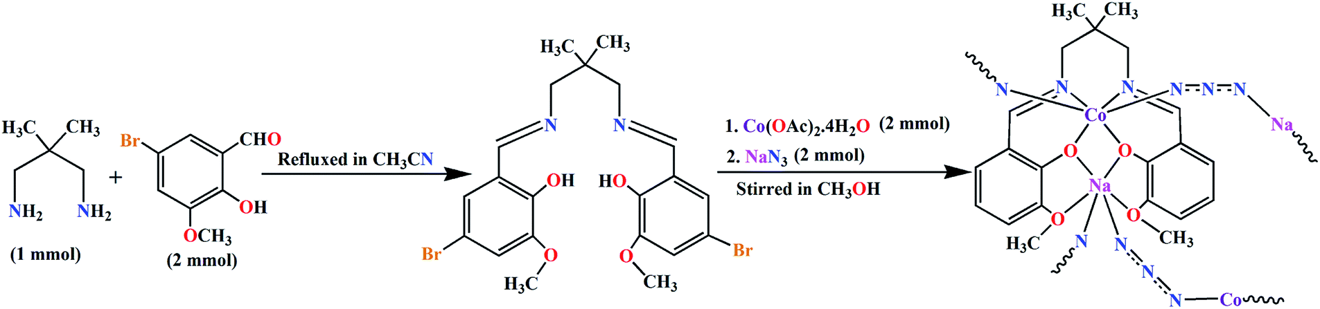
The potentially hexadentate Schiff base ligand, H2L, was synthesized by the 1![[thin space (1/6-em)]](https://www.rsc.org/images/entities/char_2009.gif) :2 condensation of 2,2-dimethyl-1,3-propanediamine with 5-bromo-3-methoxysalicylaldehyde in acetonitrile following the literature method.23,24 The acetonitrile solution of ligand (H2L) was then made to react with cobalt(II) acetate tetrahydrate and sodium azide to prepare the polymeric complex, [(N3)CoLNa(N3)]n, containing the potentially hexadentate deprotonated Schiff base ligand and coordinated azide as co-ligand (Scheme 1). Single crystal X-ray class dark brown single crystals of the complex were obtained from the 1:1 methanol–acetonitrile solution.
:2 condensation of 2,2-dimethyl-1,3-propanediamine with 5-bromo-3-methoxysalicylaldehyde in acetonitrile following the literature method.23,24 The acetonitrile solution of ligand (H2L) was then made to react with cobalt(II) acetate tetrahydrate and sodium azide to prepare the polymeric complex, [(N3)CoLNa(N3)]n, containing the potentially hexadentate deprotonated Schiff base ligand and coordinated azide as co-ligand (Scheme 1). Single crystal X-ray class dark brown single crystals of the complex were obtained from the 1:1 methanol–acetonitrile solution.
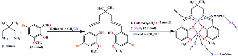 |
| | Scheme 1 Synthetic route to the complex. | |
Description of the solid-state structure
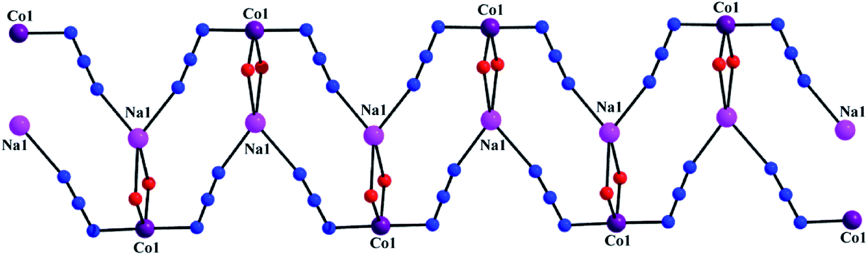
Single crystal X-ray crystallographic data analysis reveals that the complex crystallizes in the monoclinic P21/c space group and presents a 1D coordination network. The complex consists of a zigzag chain assembly with the repeating hetero-binuclear neutral unit, [(N3)CoLNa(N3)], joined through two end-to-end azide bridge. In each hetero-binuclear unit, the cobalt(III) centre resides in the inner salen-type cavity, while sodium centre resides in the open and larger position of the deprotonated compartmental Schiff base ligand, L2−. A perspective view of the complex is illustrated in Fig. 1. The metal centers are bridged by two phenoxo oxygen atoms, O(1) and O(2), of the Schiff base ligand, forming a CoO2Na core. Within the core Co(1)–Na(1) distance is 3.453 Å and bridging angles, Co(1)–O(1)–Na(1) and Co(1)–O(2)–Na(1), are 106.58° and 106.16°, respectively. All these angles and distances are comparable with previously reported similar type heteronuclear complexes.25,26 In each hetero-binuclear unit both cobalt(III) and sodium centres are present in six-coordinate environments. The cobalt(III) centre is coordinated by two imine nitrogen atoms, N(1) and N(2), and two phenoxo oxygen atoms, O(1) and O(2), of the deprotonated Schiff base ligand. One end-to-end bridged azide nitrogen atom, N(3) occupies the fifth coordination site. The remaining coordination site of cobalt(III) is occupied by one nitrogen atom, N(8)a from a symmetry related {symmetry transformation: a = x,1/2 − y,−1/2 + z} end-to-end bridged azide co-ligand to form a distorted octahedral geometry. While sodium centre is coordinated by two phenoxo oxygen atoms, O(1) and O(2), and two methoxy oxygen atoms, O(3) and O(4). The remaining two coordination sites are occupied by two end-to-end bridged azide nitrogen atoms, N(5)a and N(6). The bond angles around cobalt(III) centre are slightly distorted from the ideal values of 90° (for cis angles) and 180° (for trans angles) for the octahedral geometry, indicating the coordination geometry to be slightly distorted in nature. On the contrary, bond angles around sodium centre are highly deviated from the ideal values, referring a highly distorted geometry around the alkali metal centre. The packing diagram indicates that hetero-binuclear units are hold together to form a one-dimensional infinite zigzag chain through two end-to-end azide bridge between cobalt(III)–sodium centres (Fig. 2). The saturated six-membered chelate ring [Co(1)–N(1)–C(9)–C(10)–C(11)–N(2)] has an half-chair conformation with puckering parameters27,28 Q = 0.532(4) Å, θ = 22.5(3)° and ϕ = 173.8(9)°.
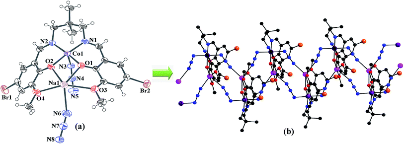 |
| | Fig. 1 (a) ORTEP diagram with 40% probability ellipsoid of hetero-binuclear unit of the complex with the corresponding atom labeling scheme; (b) polymeric chain of the complex. Hydrogen atoms are omitted for clarity. | |
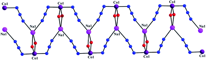 |
| | Fig. 2 One-dimensional infinite zigzag chain through two end-to-end azide bridge between cobalt(III)–sodium centres. | |
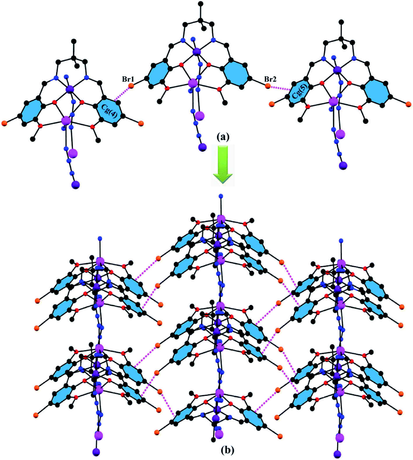
Except for the end-to-end azide bridge between the hetero-binuclear units, there are some other interesting bromine⋯π interactions in the solid state of the complex. Bromine atoms, Br(1), attached to phenyl carbon atom, C(17), and Br(2), attached to phenyl carbon atom, C(4), are involved in intermolecular bromine⋯π interaction with the symmetry related (1 + x,y,1 + z) phenyl ring, Cg4 [C(2)-C(3)-C(4)-C(5)-C(6)-C(7)] and symmetry related (−1 + x,y,z) phenyl ring, Cg5 [C(15)-C(16)-C(17)-C(18)-C(19)-C(20)]. The complex forms a 2D sheet structure by these interactions (Fig. 3). The details of these bromine⋯π interactions are summarized in Table 1. It should be emphasized that C–Br⋯π interactions have been described in several theoretical29,30 and experimental works.31 Especially relevant is the existence of Br⋯π interactions in the cytochrome P 450 active site.32 It has been demonstrated that this interaction has a crucial role in substrate selectivity and orientation in the active site. The geometrical features of the Br⋯π interaction are comparable to those already reported in the aforementioned experimental and theoretical works.
 |
| | Fig. 3 (a) Intermolecular bromine⋯π interaction in the complex; (b) formation of 2D sheet structure through intermolecular bromine⋯π interactions. | |
Table 1 Geometric features (distances in Å and angles in °) of the Br⋯π interactions obtained for the complexa
| C–Br⋯Cg(ring) |
Br⋯Cg (Å) |
C–Br⋯Cg (°) |
C⋯Cg (Å) |
| Symmetry transformations: b = 1 + x,y,1 + z and c = −1 + x,y,z. Cg(4) = centre of gravity of the ring [C(2)-C(3)-C(4)-C(5)-C(6)-C(7)] and Cg(5) = centre of gravity of the ring [C(15)-C(16)-C(17)-C(18)-C(19)-C(20)]. |
| C(17)–Br(1)⋯Cg(4)b |
3.6938(14) |
160.55(10) |
5.523(4) |
| C(4)–Br(2)⋯Cg(5)c |
3.6263(15) |
159.87(11) |
5.453(3) |
Optical characterization
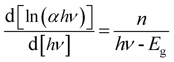
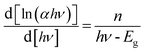
To measure the optical band gap, the UV-vis absorption spectra of the complex is recorded and shown in Fig. 4 (inset). The optical band gap energy (Eg) of the complex is calculated from Tauc's equation:33,34Here, A is a constant which is considered as 1 for general case. Absorption coefficient is denoted by α and band gap is represented by Eg. h is Planck's constant, ν is the frequency of light and the exponent n is the electron transition processes dependent constant. The plot of (αhν)2 vs. hν of the synthesized complex is portrayed in Fig. 4. The value of exponent n was taken as ½ for direct band gap. To check the value of n as ½, eqn (1) may be written as:35| |
 | (2) |
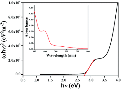 |
| | Fig. 4 Tauc's plot and UV-vis absorption spectra (inset) of the complex. | |
In the plot of d[ln(αhν)]/d[hν] versus hν (Fig. 5), a discontinuity is observed. The discontinuity at a particular energy provides the approximate value of band gap (2.81 eV). Using the value of approximate band gap (Eg), ln[(αhν)] vs. ln[hν − Eg] is plotted (inset of Fig. 5). The value of n is then obtained from the slope of the curve. Here the slope (∼0.5) proposes that the transition is directly allowed for this material. The value of optical direct band gap of the complex is evaluated as 2.74 eV from Tauc's plot.
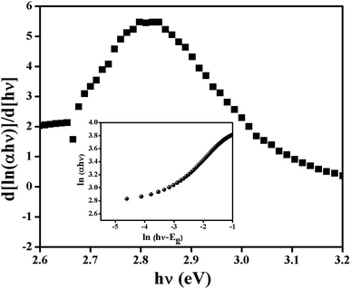 |
| | Fig. 5 d[ln(αhγ)]/d[hγ] vs. hγ and ln(αhγ) vs. ln(hγ − Eg) plot. | |
Electrical characterization
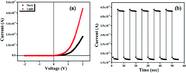
Fig. 6a shows the current–voltage characteristics of ITO/complex/Al device under dark and photo illumination condition.
 |
| | Fig. 6 (a) Current–Voltage (I–V) characteristic curve for the complex under dark and light condition; (b) transient photocurrent response. | |
Both the characteristic curves indicate the rectifying nature, with on/off current ratio 25.57 under dark and 137.49 under light at applied bias potential ± 2.0 V. The I–V characteristic curves were analyzed by the thermionic emission (TE) theory.36 Room temperature conductivity of the device under dark and illumination condition was calculated as 0.88 × 10⁻⁸ Sm−1 and 2.38 × 10⁻⁸ Sm−1. The photosensitivity of the device was found to be 1.45 at 1000 W m−2 illumination. For investigation of the photo detector response, we measured the transient photocurrent of the device under an illumination of 1000 W m−2 at bias voltage +2 V, which is represented in Fig. 6b. This transient photocurrent response mainly discloses the conductance value and the number of free carrier produce at the time of light irradiation in the semiconductor.37
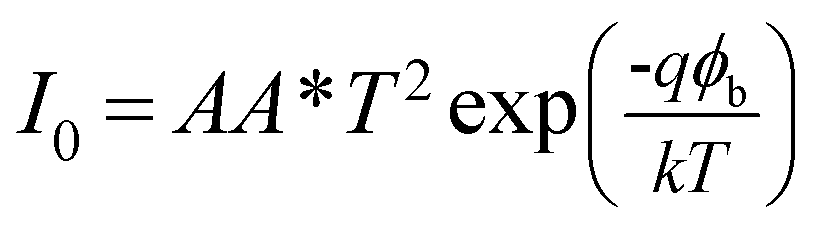
The diode analysis was performed with the help of following equations based on TE theory
| |
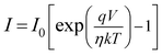 | (3) |
| |
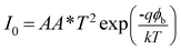 | (4) |
| |
 | (5) |
where
I0,
q,
k,
T,
A,
A*,
η and
ϕb stand for the reverse saturation current, electronic charge, Boltzmann constant, absolute temperature, the effective diode area, Richardson constant, ideality factor and the barrier potential height respectively. The effective diode area was considered as 7.065 × 10
−6 m
2 and the Richardson constant was considered as 1.20 × 10
6 A K
−2 m
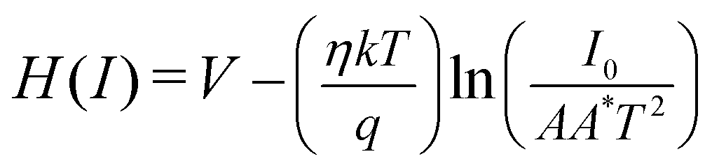
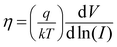
−2. The series resistance, ideality factor and barrier potential height is determined by using Cheung's equations
38,39| |
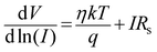 | (6) |
| |
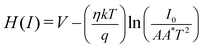 | (7) |
The series resistance and ideality factor was determined from the slope and intercept of dV/dln(I) vs. I plot for dark and light condition, which is portrayed in Fig. 7. The potential barrier height was evaluated from the y-axis intercept of H(I) vs. I curve (Fig. 7). The slope of this plot also furnished a second determination of the series resistance. The obtained values of ideality factor, barrier height and series resistance are listed in Table 2. The ideality factor of the device under dark condition indicated the deviation from ideal behavior due to high probability of electron and hole recombination in the depletion region or occurrence of tunneling current or presence of inhomogenities of Schottky barrier height or existence of interface states40,41 whereas, upon light irradiation the value approached to unity. We have also studied temperature and thickness dependent current–voltage characteristics for our synthesized complex (see ESI†).
 |
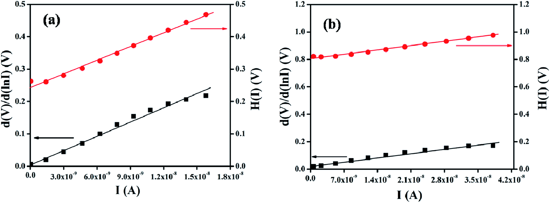
| | Fig. 7 dV/dlnI vs. I and H(I) vs. I curve for the complex based Schottky barrier diode under (a) dark and (b) photo condition. | |
Table 2 Schottky diode parameters
| Measured condition |
Conductivity (σ) (Sm−1) |
Photosensitivity |
d(V)/d(lnI) vs. I graph |
H(I) vs. I graph |
| Ideality factor (η) |
Series resistance (RS) (ohm) |
Barrier height (ϕb) (eV) |
Series resistance (RS) (ohm) |
| Dark |
0.88 × 10⁻⁸ |
1.45 |
0.27 |
1.45 × 10⁷ |
0.90 |
1.40 × 10⁷ |
| Light |
2.38 × 10⁻⁸ |
0.91 |
4.39 × 10⁶ |
0.87 |
4.41 × 10⁶ |
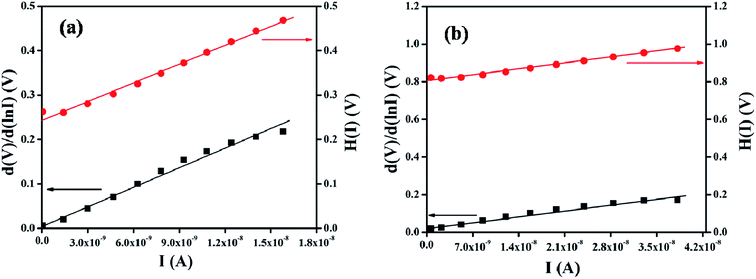
To get better insight of the charge transport mechanism in the junction we have analyzed the I–V characteristic by employing space charge limited current (SCLC) theory. In this purpose we have looked into the logarithm current vs. voltage (I–V) curves under dark and photo illumination (Fig. 8).
 |
| | Fig. 8 logI versus logV plot under dark and light condition. | |
The region-I indicates the ohmic behavior (since I ∞ V) in the low voltage region. This came across due to the occurrence of series resistance of the device, whereas, the region II corresponds to the higher ordered magnitude of slope, exhibits variation of current with square of forward bias voltage (I ∞ V2). In this region the current originated from space charge, designated as space charge limit current (SCLC) mechanism by discrete trapping level. The region-III is influenced by SCLC mechanism (I ∞ Vm) due to exponential distribution of traps. The electron mobility under dark and photo illumination was estimated as 7.90 × 10⁻¹⁰ m2 V−1 s−1 and 22.59 × 10⁻¹⁰ m2 V−1 s−1 from I vs. V2 plot (Fig. 9) using by Mott-Gurney space-charge-limited-current (SCLC) equation:42,43
| |
 | (9) |
where,
I is the current density,
ε0 is the permittivity of free space and
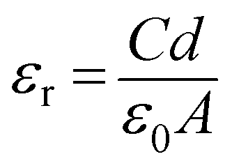
εr the dielectric constant. The value of dielectric constant of the material was measured as 3.43 from capacitance
vs. frequency plot (
C–
f) (
Fig. 10) by using the equation:
44| |
 | (10) |
where,
C is the capacitance (at saturation),
d is the thickness of the film and rest are same as defined previously.
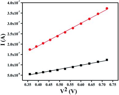 |
| | Fig. 9 I vs. V2 plot of SCLC region under dark and photo condition. | |
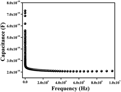 |
| | Fig. 10 Capacitance vs. frequency (C–f) plot for the complex. | |
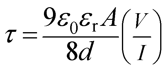
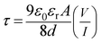
Transit time (τ) is defined as the time, which is required by a carrier to travel from anode to cathode. It can be expressed as the summation of average total time spent by each electron as a free carrier plus total time spent in the tarp.45 The transit time (τ) of the charge carrier is estimated with the help of following equation:46
| |
 | (11) |
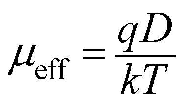
The diffusion length of the charge carrier was calculated from Einstein–Smoluchowski equation:47
| |
 | (12) |
and
| |
 | (13) |
where,
D is the diffusion co-efficient and
LD is the diffusion length of the charge carrier. It has been observed that after light soaking the mobility of the charge carrier is increased up to 185%. The longer transit time in dark condition indicates the higher trapping probabilities. Under the illumination condition lowering of transit time leads to reduce the trapping time due to the higher carrier mobility.
48,49 Diffusion length of the carriers also improved under an illumination condition, which points out that our material, can be a good potential candidate in photovoltaic device application. All the obtained values of charge transport parameters for Al/complex/ITO are listed in
Table 3.
Table 3 SCLC/charge transport parameters
| Measured condition |
SCLC conductivity (σ) (Sm−1) |
Carrier mobility (μ) × 10−10 m2 v−1 s−1 |
Transit time (τ) × 10−4 (sec) |
μτ × 10−14 (m2 v−1) |
Diffusion coefficient (D) × 10−12 (m2 s−1) |
Diffusion length (LD) (nm) |
| Dark |
2.31 × 10⁻⁷ |
7.90 |
8.55 |
67.67 |
20.39 |
186 |
| Light |
5.55 × 10⁻⁷ |
22.59 |
3.09 |
69.96 |
58.29 |
190 |
Structure–property relationship
The complex is a one-dimensional complex (Fig. 2) where the asymmetric units are bridged via end-to-end azide moieties. Intermolecular bromine⋯π interaction in the complex form a 2D sheet structure (Fig. 3). Formation of this supramolecular structure is most likely responsible for the photosensitivity of the complex. The complex can sense whether the light source is switched on or switched off (Fig. 6b, 7a, 7b, 8 and 9). Thus, it may be concluded that the complex may be used to prepare a suitable opto-electronic device with the help of which with switching of the photocurrent may be possible time after time without any drop of the on/off ratio. The complex may, therefore, find applications in the fabrication of photo switch devices. A probable justification for this activity may be given as following. The organic ligand is electron rich and may therefore act as the supplier of negative charge upon photoexcitation, while the inorganic Na–N3–Co(III) unit (which is most probably electron deficient as both sodium and cobalt are in positive oxidation states) behaves as an acceptor of electron.
Theoretical study
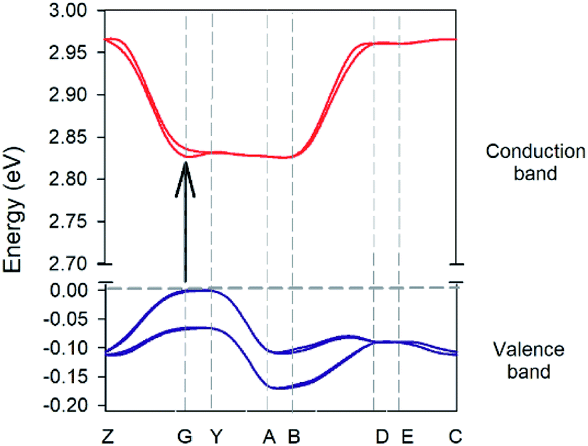
The experimental crystal lattice has been chosen as started point for optimizing the atomic positions of the complex in the solid state (see ESI for full computational details†). Crystal structure analysis has been done by standard band theory and total/partial density of states calculation, giving a band gap value of 1.80 eV. Since this value is significantly lower than the experimental one as common in theoretically predicted band gaps calculated using DFT,50 we have applied a conventional scissor operator of +0.94 eV to the theoretical properties reported in this work. Fig. 11 shows the plot of the valence and conduction bands which indicates that the complex is a direct semiconductor.
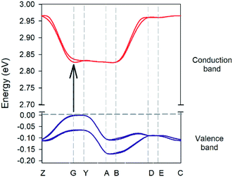 |
| | Fig. 11 Electronic band structure of the ground state of the complex crystal. Points of high symmetry in the first Brillouin zone are labeled as follows: Z = (0, 0, 0.5); G = (0, 0, 0); Y = (0, 0.5, 0); A = (−0.5, 0.5, 0); B = (−0.5, 0, 0); D = (−0.5, 0, 0.5); E = (−0.5, 0.5, 0.5) and C = (0, 0.5, 0.5). The energy positions of the all the conduction bands are shifted upward by 0.94 eV through a scissors operator. | |
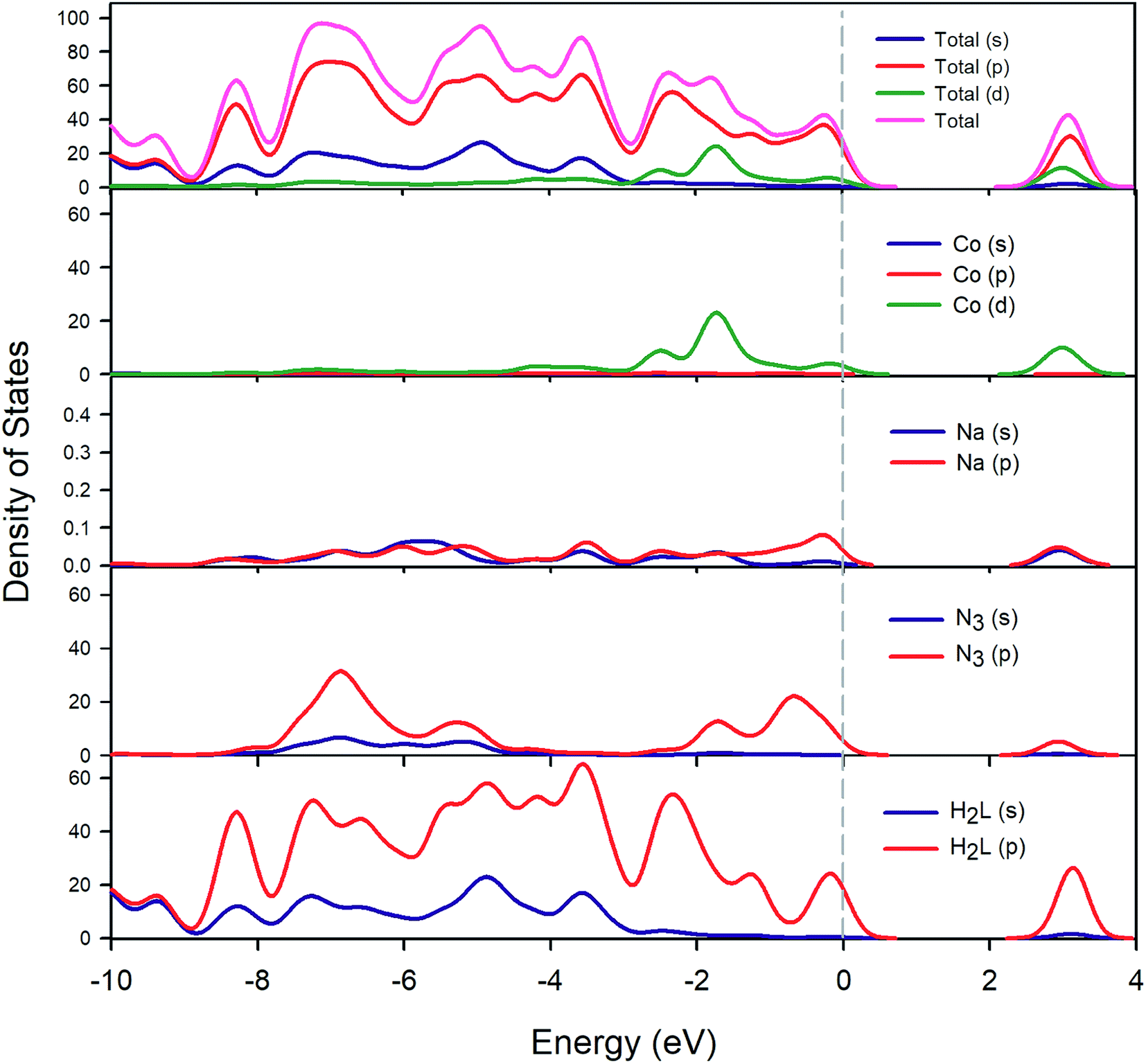
The total and partial DOS calculation shown in Fig. 12 reveals that the valence bands are mainly dominated by the p-orbitals of the ligands (both organic ligand and azide) and to a lesser extent by the d-orbitals of the cobalt atoms. In addition, the main contributors to the conduction band are the p-orbitals of the Schiff base ligand (H2L) and the d-orbitals of the cobalt atoms. The azide ligand and sodium cations have little influence on the conduction bands.
 |
| | Fig. 12 Calculated total and partial density of states of cobalt (Co), sodium (Na), azide (N3) and Schiff base (H2L). | |
Fig. 13 and 14 represent the optical properties of the solid-state material. They provide some information regarding the character of the bands. In each material, the frequency dependence of an incident photon can be studied by computing the dielectric function ε(ω). The real part of ε(ω) gives information about the polarization degree of the material upon the application of an electric field. The imaginary part is a good indicator of the absorption in the material of the incident photon. We have used the computed band structure to measure the optical response. To do so, we have selected a photon energy range of 0 to 16 eV. The peaks can be assigned to electronic transitions from the top of the valence band to the low energy in the conduction band. Due to the anisotropy of the crystal we have decomposed the dielectric constant in three main directions where the light may fall on the crystal (εxx, εyy, εzz) (see ESI Fig. S1†). In this case, two of the directions (blue and green line of Fig. 13) represent a first maximum in 2.9 eV, while the εzz direction is three times lower than the rest of the components. The imaginary parts of dielectric functions have a main peak for complex at 4.5 eV. Fig. 14 represents the optical conductivity [σ(ω)]. This property is useful to analyze how the conductivity of the material changes upon illumination. As can be seen, near of 2.0 eV (black dashed line) σ(ω) starts to grow finding the first maximum at 2.9 eV (blue dashed line). The electrical conductivity and, concomitantly, the photoconductivity of the material increase as a consequence of photon absorption.
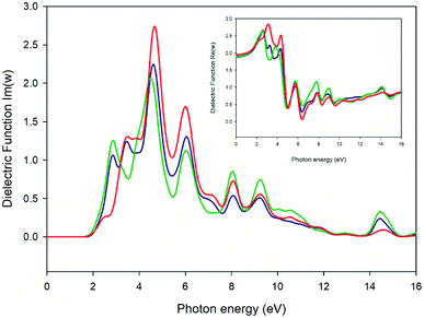 |
| | Fig. 13 Plot of real (small square) and imaginary (big square) parts of the dielectric function versus the photon energy of the crystal. Blue, green and red lines specify the incident direction of unpolarized radiation in the ‘x’, ‘y’ and ‘z’ directions of the crystal, respectively. | |
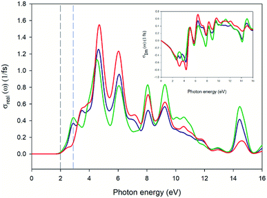 |
| | Fig. 14 Plot of real (big square) and imaginary (small square) parts of optical conductivity versus the photon energy of the crystal. Blue, green and red lines specify the incident direction of unpolarized radiation in the ‘x’, ‘y’ and ‘z’ directions of the crystal, respectively. | |
Conclusions
In this work, we illustrate the opto-electronic properties of a new heteronuclear cobalt(III)–sodium complex. The band gap of this semiconductor material in the solid state has been determined by experimental as well as DFT calculations and it confirms that it is a direct semiconductor. We have also shown the potential of this heteronuclear complex in fabricating a photosensitive Schottky device. Theoretical studies have been used to rationalize the experimental observations and to provide an explanation to the enhanced conductivity of the complex upon illumination. It is a promising candidate to have applications in CP semiconducting research and in the fabrication of optoelectronic devices.
Conflicts of interest
There are no conflicts to declare.
Acknowledgements
K. G. expresses his gratitude to UGC, India, for awarding a Senior Research Fellowship. Crystallographic data was collected at the DST-FIST, India funded Single Crystal Diffractometer Facility at the Department of Chemistry, Jadavpur University. P. P. R. gratefully acknowledges the financial support of this work by SERB-DST, Govt. of India (Sanction No. EMR/2016/005387, Dated – 24.07.2017). AF thanks MINECO/AEI of Spain (Project CTQ2017-85821-R, FEDER funds) for financial support. We also thank the CTI (UIB) for computational facilities.
References
- S. S. Park, E. R. Hontz, L. Sun, C. H. Hendon, A. Walsh, T. V. Voorhis and M. Dincă, J. Am. Chem. Soc., 2015, 54, 1774–1777 CrossRef.
- W. Xia, A. Mahmood, R. Zou and Q. Xu, Energy Environ. Sci., 2015, 8, 1837–1866 RSC.
- L. Sun, M. G. Campbell and M. Dincă, Angew. Chem., Int. Ed., 2016, 55, 3566–3579 CrossRef CAS PubMed.
- M. Sadakiyo, T. Yamada and H. Kitagawa, J. Am. Chem. Soc., 2009, 131, 9906–9907 CrossRef CAS PubMed.
- T. Y. Ma, S. Dai, M. Jaroniec and S. Z. Qiao, J. Am. Chem. Soc., 2014, 136, 13925–13931 CrossRef CAS PubMed.
- B. Chen, L. Wang, F. Zapata, G. Qian and E. B. Lobkovsky, J. Am. Chem. Soc., 2008, 130, 6718–6719 CrossRef CAS.
- V. Stavila, A. A. Talin and M. D. Allendorf, Chem. Soc. Rev., 2014, 43, 5994–6010 RSC.
- P. K. Ng, X. Gong, S. H. Chan, L. S. M. Lam and W. K. Chan, Chem.–Eur. J., 2001, 7, 4358–4367 CrossRef CAS.
- S. Roy, M. Das, A. Bandyopadhyay, S. K. Pati, P. P. Ray and T. K. Maji, J. Phys. Chem. C, 2017, 121, 23803–23810 CrossRef CAS.
- S. Roy, A. Dey, P. P. Ray, J. Ortega-Castro, A. Frontera and S. Chattopadhyay, Chem. Commun., 2015, 51, 12974–12976 RSC.
- S. Khan, S. Halder, P. P. Ray, S. Herrero, R. González-Prieto, M. G. B. Drew and S. Chattopadhyay, Cryst. Growth Des., 2018, 18, 651–659 CrossRef CAS.
- B. Bhattacharya, A. Layek, Md. M. Alam, D. K. Maity, S. Chakrabarti, P. P. Ray and D. Ghoshal, Chem. Commun., 2014, 50, 7858–7861 RSC.
- B. Bhattacharya, D. K. Maity, A. Layek, Sk. Jahiruddin, A. Halder, A. Dey, S. Ghosh, C. Chowdhury, A. Datta, P. P. Ray and D. Ghoshal, CrystEngComm, 2016, 18, 5754–5763 RSC.
- S. Halder, A. Dey, A. Bhattacharjee, J. Ortega-Castro, A. Frontera, P. P. Ray and P. Roy, Dalton Trans., 2017, 46, 11239–11249 RSC.
- S. Halder, A. Layek, K. Ghosh, C. Rizzoli, P. P. Ray and P. Roy, Dalton Trans., 2015, 44, 16149–16155 RSC.
- P. Ghorai, A. Dey, P. Brandão, J. Ortega-Castro, A. Bauzá, A. Frontera, P. P. Ray and A. Saha, Dalton Trans., 2017, 46, 13531–13543 RSC.
- F. Ahmed, S. Halder, B. Dutta, S. Islam, C. Sen, S. Kundu, C. Sinha, P. P. Ray and M. H. Mir, New J. Chem., 2017, 41, 11317–11323 RSC.
- K. Naskar, A. Dey, B. Dutta, F. Ahmed, C. Sen, M. H. Mir, P. P. Roy and C. Sinha, Cryst. Growth Des., 2017, 17, 3267–3276 CrossRef CAS.
- S. Roy, S. Halder, M. G. B. Drew, P. P. Ray and S. Chattopadhyay, New J. Chem., 2018, 42, 15295–15305 RSC.
- T. Zhang and W. Lin, Chem. Soc. Rev., 2014, 43, 5982–5993 RSC.
- L. Sun, L. Hammarström, B. Åkermark and S. Styring, Chem. Soc. Rev., 2001, 30, 36–49 RSC.
- P. Du and R. Eisenberg, Energy Environ. Sci., 2012, 5, 6012–6021 RSC.
- A. S. Ogunlaja, W. Chidawanyika, E. Antunes, M. A. Fernandes, T. Nyokong, N. Tortoa and Z. R. Tshentu, Dalton Trans., 2012, 41, 13908–13918 RSC.
- H.-C. Fang, Y.-Y. Ge, Y. Ying, S.-R. Zheng, Q.-G. Zhan, Z.-Y. Zhou, L. Chen and Y.-P. Cai, CrystEngComm, 2010, 12, 4012–4016 RSC.
- E. K. Brechin, L. M. Gilby, R. O. Gould, S. G. Harris, S. Parsons and R. E. P. Winpenny, J. Chem. Soc., Dalton Trans., 1998, 2657–2664 RSC.
- S. S. Tandon, S. D. Bunge, R. Rakosi, Z. Xu and L. K. Thompson, Dalton Trans., 2009, 6536–6551 RSC.
- D. Cremer and J. A. Pople, J. Am. Chem. Soc., 1975, 97, 1354–1358 CrossRef CAS.
- A. D. Hill and P. J. Reilly, J. Chem. Inf. Model., 2007, 47, 1031–1035 CrossRef CAS.
- I. S. Youn, D. Y. Kim, W. J. Cho, J. M. L. Madridejos, H. M. Lee, M. Kołaski, J. Lee, C. Baig, S. K. Shin, M. Filatov and K. S. Kim, J. Phys. Chem. A, 2016, 120, 9305–9314 CrossRef CAS.
- D. Y. Kim, J. M. L. Madridejos, M. Ha, J.-H. Kim, D. C. Yang, C. Baig and K. S. Kim, Chem. Commun., 2017, 53, 6140–6143 RSC.
- M. M. Naseer, A. Bauzá, H. Alnasr, K. Jurkschat and A. Frontera, CrystEngComm, 2018, 20, 3251–3257 RSC.
- M. B. Shah, J. Liu, Q. Zhang, C. D. Stout and J. R. Halpert, ACS Chem. Biol., 2017, 12, 1204–1210 CrossRef CAS.
- R. Pandiyan, V. Micheli, D. Ristic, R. Bartali, G. Pepponi, M. Barozzi, G. Gottardi, M. Ferrari and N. Laidani, J. Mater. Chem., 2012, 22, 22424–22432 RSC.
- J. Tauc, Amorphous and Liquid Semiconductors, Plenum Press, New York, 1974 Search PubMed.
- F. Yakuphanoglu, B. F. Senkal and A. Sarac, J. Electron. Mater., 2008, 37, 930–934 CrossRef CAS.
- E. H. Rhoderick and R. H. Williams, Metal-Semiconductor Contacts, Clarendon Press, Oxford, 2nd edn, 1988 Search PubMed.
- L. P. Wu, Y. L. Zhang, L. Z. Long, C. P. Cen and X. J. Li, RSC Adv., 2014, 4, 20716–20721 RSC.
- S. K. Cheung and N. W. Cheung, Appl. Phys. Lett., 1986, 49, 85–87 CrossRef CAS.
- M. Benhaliliba, J. New Technol. Mater., 2015, 05, 24–27 CrossRef CAS.
- R. K. Gupta and F. Yakuphanoglu, Sol. Energy, 2012, 86, 1539–1545 CrossRef CAS.
- M. Campos, L. O. S. Bulhões and C. A. Lindino, Sens. Actuators, A, 2000, 87, 67–71 CrossRef CAS.
- M. Soylu and B. Abay, Phys. E, 2010, 43, 534–538 CrossRef CAS.
- M. Das, J. Datta, R. Jana, S. Sil, S. Halder and P. P. Ray, New J. Chem., 2017, 41, 5476–5486 RSC.
- S. Middya, A. Layek, A. Dey, J. Datta, M. Das, C. Banerjee and P. P. Ray, Chem. Phys. Lett., 2014, 610–611, 39–44 CrossRef CAS.
- J. Datta, M. Das, A. Dey, S. Halder, S. Sil and P. P. Ray, Appl. Surf. Sci., 2017, 420, 566–578 CrossRef CAS.
- T. Ye, H. Shi, N. Phan-Thien, C. T. Lim and Y. Li, Soft Matter, 2018, 14, 533–545 RSC.
- J. R. Sangoro, C. Iacob, W. K. Kipnusu, M. Jasiurkowska, R. Valiullin, C. Friedrich, J. Kärger and F. Kremer, Soft Matter, 2011, 7, 10565–10568 RSC.
- K. C. Kao, Dielectric Phenomena in Solids, Elsevier Inc., San Diego, California, 2004 Search PubMed.
- S. V. Kershaw, L. Jing, X. Huang, M. Gao and A. L. Rogach, Mater. Horiz., 2017, 4, 155–205 RSC.
- M. Shishkin and G. Kresse, Phys. Rev. B: Condens. Matter Mater. Phys., 2007, 75, 235102 CrossRef.
Footnote |
| † Electronic supplementary information (ESI) available: The complete experimental section, analysis of Hirshfeld surfaces, X-ray diffraction of powdered material, spectral and magnetic characterization of the complex are given. CCDC 1866271. For ESI and crystallographic data in CIF or other electronic format see DOI: 10.1039/c9ra06354d |
|
| This journal is © The Royal Society of Chemistry 2019 |
Click here to see how this site uses Cookies. View our privacy policy here. 
 Open Access Article
 This Open Access Article is licensed under a Creative Commons Attribution-Non Commercial 3.0 Unported Licence
 b,
Joaquín Ortega-Castroc,
Antonio Frontera
b,
Joaquín Ortega-Castroc,
Antonio Frontera