
 Open Access Article
 This Open Access Article is licensed under a Creative Commons Attribution-Non Commercial 3.0 Unported Licence
Preparation of CdTe superparticles for white light-emitting diodes without Förster resonance energy transfer†
Haoyang
Zou
a,
Deli
Wang
*b,
Baijuan
Gong
*c and
Yi
Liu
 *a
*a
aState Key Laboratory of Supramolecular Structure and Materials, Jilin University, Changchun 130012, P. R. China. E-mail: yiliuchem@jlu.edu.cn
bSchool of Life Sciences, Jilin University, Changchun 130012, P. R. China. E-mail: wangdl@jlu.edu.cn
cDepartment of Orthodontics, School and Hospital of Stomatology, Jilin University, #1500 Qinghua Road, Changchun, Jilin 130021, P. R. China. E-mail: gongbj@jlu.edu.cn
First published on 30th September 2019
Abstract
Due to many unique and excellent optical properties, quantum dots (QDs) have been seen as one of the most promising color conversion materials in light-emitting diodes (LEDs). However, the Förster resonance energy transfer (FRET) among different colored QDs always causes a significant red-shift of the fluorescence emission, impeding the fabrication of LEDs with predicted photoluminescence (PL) emission spectra. In this work, we take advantage of CdTe superparticles (SPs), which are assembled by CdTe QDs, as the color conversion materials for the fabrication of WLEDs. Because of their submicron size, the distance between QDs with different emissions can be large enough to avoid the FRET process. More importantly, this method provides us with an opportunity to precisely design and regulate the PL emission spectra of LEDs. By easily overlapping the individual PL spectra of CdTe SPs with different emissions, the certain ratio of their usage for fabricating LEDs with desired PL emission spectra is identified. According to this idea, a WLED with a color rendering index (CRI) of 81, luminous efficacy of 27 lm W−1, and color coordinate at (0.33, 0.34) with the color temperature of 5742 K is achieved.
Introduction
During the past decade, illumination occupied approximately 20% of the global electrical energy consumption.1 Thus, the exploration of novel light sources in response to the energy shortage and irreversible climate change is urgent and necessary.2 Because of the advantages in lifetime, efficiency, cost, and eco-friendliness, light-emitting diode (LED) technology exhibits huge potential compared with old-fashioned light sources, such as incandescent, fluorescent, and high-intensity discharge (HID), in the field of home and office illumination, street lighting, automotive lights, and backlighting in displays.3,4 Currently, the commercial white LEDs (WLEDs) are normally fabricated by coating yellow-emitting rare-earth based phosphors (cerium-doped yttrium aluminum garnet) on a blue-violet light-emitting InGaN/GaN chip.5–9 Despite rare-earth based phosphors being good at photon conversion, they still suffer from problems such as being unstable against photo-oxidation or chemical environments.10 In particular, their color deficiencies in green and red regions always cause WLEDs to have low color rendition and a poor spectral match with the spectral sensitivity of the human eye.11 Thanks to their intrinsic optical properties including size-dependent and tunable photoluminescence (PL), broad excitation spectra, narrow PL spectra, high PL quantum yields (QYs), and good photochemical stability, quantum dots (QDs) are seen as the competitive alternative color conversion materials to endow WLEDs with a wider color gamut, higher luminous efficacy and durability, but lower cost. This concept has already given birth to a new industry named QD LEDs (QLEDs).12–15Typically, white light is generated by combining red, green, and blue light under a specific ratio. Thus, adjusting the ratio of red- and green-emitting QDs on the blue-emitting chip is of crucial importance.16 However, this adjustment process is highly challenging due to the existence of Förster resonance energy transfer (FRET) between QDs with different emissions, which always cause a significant red-shift of the final color from the desired color and a decrease in the luminous efficiency of WLEDs.17,18 It is known that FRET is a non-radiative energy transfer process from a fluorescent donor to a lower energy acceptor via long-range dipole–dipole interactions.19,20 Significant FRET can be observed for donor–acceptor distance in the range of 1–10 nm.21 Although FRET is very useful in the areas of fluorescent sensor and bioimaging, it is undesirable in panchromatic displays and illumination because extra shorter wavelength emitters must be added to compensate for the energy transferred to longer wavelength emitters. Since there is no theory can quantitatively predict the PL emission spectra alteration derived from FRET, a lot of experimental attempts are required to adjust the fluorescence intensity ratio of red- and green-emitting QDs to a specific value. Previous works have reported some strategies to alleviate the FRET process.22–24 Yang employed electrospinning to block the aggregation of CdTe QDs in polymer chains, then fabricated highly fluorescent 1D nanofibers without FRET.25 Chiang used poly(methyl methacrylate-co-acrylic acid) (PMMA-co-MA) as the matrix to separate green- and red-emitting QDs, then realized the fabrication of WLEDs with predictable PL emission spectra.26
Besides the strategies above, utilizing the self-assembly technology to pre-construct the submicron-structures of single colored QDs is another way to enlarge the distance between QDs with different emissions, efficiently preventing the FRET process sourcing from their aggregation. In this study, we demonstrate a fabrication of fluorescent superparticles (SPs) by using aqueous synthesized CdTe QDs and oil-in-water (O/W) microemulsions as the building blocks and template.27 The size of the as-prepared CdTe SPs can be tunable from 80 to 330 nm. We find that the SP nanostructure can efficiently eliminate the FRET process by enlarging the distance between QDs with different emissions. In contrast, the mixture of CdTe QDs with different emissions exhibits obvious red-shift derived from FRET due to their nanoscale size and short inter-QD distance. At last, green-, yellow-, and red-emitting CdTe SP powders are mixed with poly(vinyl alcohol) (PVA), coated on a GaN LED chip for the fabrication of WLEDs (Scheme 1b). The resulting WLEDs possess the color rendering index (CRI) of 81, luminous efficacy of 27 lm W−1, and color coordinate at (0.34, 0.33) with the color temperature of 5742 K, respectively.
 | ||
| Scheme 1 Schematic representation for the fabrication of CdTe SPs (a) and WLED device based on CdTe SPs (b). | ||
Experimental section
Materials
Tellurium powder (∼200 mesh, 99.8%), 3-mercaptopropionic acid (MPA, 99+%), didodecyldimethylammonium bromide (DDAB, 98%), dodecyltrimethylammonium bromide (DTAB, 98%) poly(vinyl alcohol) (PVA, Mn = 5000) are purchased from Aldrich. CdCl2 (99%) and NaBH4 (96%) are commercially available products and used as received. Polydimethylsiloxane (PDMS) elastomer kits (Sylgard 184) are purchased from Dow Corning (Midland, MI).Synthesis of aqueous CdTe QDs
The synthesis of aqueous CdTe QDs follows our previous work.28 In brief, MPA-stabilized CdTe precursors are foremost synthesized by injecting freshly prepared NaHTe aqueous solution into N2-saturated CdCl2 solution at pH = 9.5 in the presence of MPA at room temperature. The concentration of precursors is 5 mM referring to Cd2+. The molar ratio of Cd2+/MPA/HTe− is 1![[thin space (1/6-em)]](https://www.rsc.org/images/entities/char_2009.gif) :2.4:0.2. The precursors are refluxed at 100 °C for a specific duration to obtain QDs with the desired PL emitting color.
:2.4:0.2. The precursors are refluxed at 100 °C for a specific duration to obtain QDs with the desired PL emitting color.
Synthesis of DDAB-capped CdTe QDs
50 ml CdTe QDs aqueous solution is mixed with 5 ml chloroform containing 250 mg DDAB, followed by vigorous stirring for 10 min to extract QDs from water to chloroform. Then the chloroform phase is separated and DDAB-capped CdTe QDs are obtained.Synthesis of CdTe SPs
1 ml chloroform solution of DDAB-capped CdTe QDs is mixed with 5 ml water containing 20 mg DTAB. The mixture is heated at 45 °C under vigorous stirring. CdTe SPs are obtained after removing chloroform by evaporation.Preparation of CdTe-PVA films
First, 0.05 g PVA is dissolved in 1 ml deionized water. 1 ml 5 mg ml−1 CdTe QDs/SPs aqueous solution is added to PVA aqueous solution. All upward chemicals are mixed under stirring at 400 rpm for at least 12 h. Then 0.4 ml of the above solution is dropped on a 1 × 1 cm hydroxylated quartz plate. The quartz plate is under vacuum for 12 h to achieve CdTe-PVA composite films.Fabrication of LEDs from CdTe SPs
The InGaN LED chips without phosphor coating are purchased from Shen Zhen Hongcai Electronics Co., Ltd. The operating voltage is 3.0 V while the emission of the LED chip is centered at 450 nm. First, 0.2 ml PDMS is dropped to the center of the LED chip, spin-coated at 2000 rpm for 60 s, and dried at 80 °C for 30 min. Then 1.5 ml aqueous solution containing 10 mg CdTe SPs and 100 mg PVA are prepared under stirring at 400 rpm for 24 h. Subsequently, the resulting solution is filled into the cup-shaped void of the LED chip. The chip is put in a vacuum chamber to remove water. After vacuuming for 12 h, the LEDs based on CdTe SPs are produced.Characterization
UV-visible absorption spectra were measured using a Lambda 800 UV-vis spectrophotometer. Photoluminescent (PL) spectroscopy was measured with a Shimadzu RF-5301 PC spectrophotometer. Dynamic light scattering (DLS) and zeta potential measurements were performed using a Zetasizer NanoZS (Malvern Instruments). The excitation wavelength was 400 nm. PL quantum yields (PLQYs) of QDs were calculated at room temperature using quinine in 0.5 mol L−1 H2SO4 aqueous solution as the reference. Transmission electron microscopy (TEM) was performed using a Hitachi H-800 electron microscope at an acceleration voltage of 200 kV with a CCD camera. High-resolution TEM (HRTEM) imaging was performed by a JEM-2100F electron microscope at 200 kV. A scanning electron microscope (SEM) image was implemented with a JEOL FESEM 6700F electron microscope with primary electron energy of 3 kV. X-ray powder diffraction (XRD) investigation was taken using a Siemens D5005 diffractometer. Inductive coupled plasma emission spectrometry (ICP) was performed with a PerkinElmer Optima 3300DV analyser. Luminous efficacy, CIE (Commission Internationale de L'Eclairage 1931), color temperature, and other properties of devices were taken using HAAS2000. The color of light was identified by the CIE colorimetry system. Any color could be described by the chromaticity (x, y) coordinates on the CIE diagram.Results and discussion
As shown in Scheme 1a, the overall preparative procedures of CdTe SPs involve a two-step phase transfer strategy.29 In a typical synthesis, CdTe QDs are firstly prepared by using NaHTe and MPA as Te source and capping ligand in aqueous media.28 By controlling the reflux time, the size and PL emission color of CdTe QDs are tunable (Table S1†). Furthermore, the negative charge of MPA endows CdTe QDs with the ability to absorb cationic surfactants (DDAB) through electrostatic attraction, providing driving force to modify surfactant monolayer on the surface of QDs. Due to the existence of hydrophobic alkyl chains in DDAB, DDAB-capped CdTe QDs are dispersed in chloroform instead of water. For the second step of phase transfer, the chloroform solution of DDAB-capped CdTe QDs is mixed with an aqueous solution of the second surfactant (DTAB) under vigorous stirring to form an O/W microemulsion. After the evaporation of chloroform under moderate heating (around 45 °C), the alkyl chains of both DDAB and DTAB interact through the hydrophobic–hydrophobic interaction, whereas the hydrophilic groups of DTAB spread toward aqueous media. As a result, CdTe QDs spontaneously assembled into SPs accompanied by the transfer from chloroform to water again. It is worth to mention that the surfactants in our two-step phase transfer strategy are not only limited to DDAB and DTAB. Various surfactants including sodium dodecyl sulfate (SDS) and tetraethylene glycol monooctyl ether (C8E4) are available in this process.30,31TEM, DLS, zeta potential, UV-vis absorption and PL emission spectra are used to monitor the preparative procedures of CdTe SPs.32 Red-emitting CdTe QDs with an average diameter of 4.2 nm and PLQYs of 24.1% are firstly prepared as the building blocks (Fig. 1a). The sharp feature of the absorption spectrum and the narrow full width at half maximum (fwhm) of the PL spectrum indicate their uniform size distribution (Fig. 1e and f). Because covering by MPA, the hydrodynamic diameter and zeta potential of CdTe QDs are 40.3 nm and −47.4 mV, respectively. Fig. 1b, e and f show the TEM image, UV-vis absorption and PL emission spectra of DDAB-capped CdTe QDs, from which it can be seen that the morphology, dispersity, optical properties of original CdTe QDs are well maintained without any destruction during the modification of DDAB. Following the second step of phase transfer, quasi-spherical CdTe SPs with an average diameter of 260 nm are prepared (Fig. 1d). Accordingly, their hydrodynamic diameter enlarges to 362.1 nm. In the meantime, due to the positive charge of DTAB, zeta potential of CdTe SPs changes to +54.6 mV. Moreover, since the scattering effect of their submicron size leading to an oblique baseline in the absorption spectrum, the characteristic absorption of CdTe SPs is weaker than that of CdTe QDs (Fig. 1e). Besides, a slight red-shift of the PL emitting peak coming from the close stacking of QDs in the SP structure is observed (Fig. 1f). Since the sizes of CdTe QDs prepared in colloidal solution are not ideally monodispersed but follow a Gaussian distribution. If the inter-QD distance is less than 10 nm, the small QDs potentially act as the donor but the large QDs act as the acceptor, thus the FRET from small QDs to big QDs is activated.21 Consequently, the acceptor PL is enhanced by forfeiting the donor PL, represented by the slight red-shift of the PL spectrum (Fig. 1f).
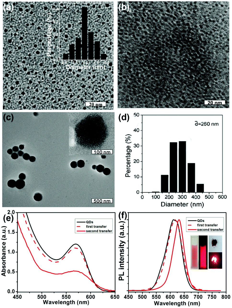 | ||
| Fig. 1 TEM images of original CdTe QDs in aqueous solution (a), DDAB-capped CdTe QDs in chloroform (b), and CdTe SPs in aqueous solution (c). Size distribution of the CdTe SPs (d). UV-vis absorption (e) and PL emission (f) spectra of the original CdTe QDs, DDAB-capped CdTe QDs, and CdTe SPs. Inset: (a) size distribution of the CdTe QDs; (f) photographs of CdTe SP solution and powder under sunlight and UV irradiation. | ||
XRD and ICP are further used to characterize the composition of CdTe QDs and SPs. As shown in Fig. S1 and Table S2,† XRD pattern of CdTe SPs exhibits a typical cubic structure, consisting with the crystal phase of original CdTe QDs. Based on Scherrer formula, the average size of CdTe QDs estimated from the broadening of the XRD pattern is 4.1 nm, which agrees well with the size obtained from TEM. Despite the molar ratio of Cd/Te in CdTe SPs is calculated to be 1.9/1, which is lower than that in original aqueous CdTe QDs (9.7/1), it almost remains constant during the second step of phase transfer. Based on the results above and previous reports, it is reasonable to believe that the formation of SPs derives from the self-assembly of QDs, while the decrease of Cd/Te molar ratio is mainly attributed to the removal of free Cd-MPA complexes during the first step of phase transfer process.33
Because the fluorescence of CdTe SPs derives from their building blocks, it is possible to deliberately adjust the PL emission color of as-prepared CdTe SPs through tuning the size of the CdTe QDs. As shown in Fig. 2, green- and yellow-emitting CdTe SPs are prepared by using 3.4 and 3.6 nm CdTe QDs as the building blocks, respectively. Notably, the diameters of CdTe SPs are irrelevant to their building blocks, but dominantly depended on the microemulsion templates. For example, following the similar synthetic procedure expect varying the size of CdTe QDs, the diameters of as-prepared CdTe SPs keep the same (Fig. S2†). However, by fixing the concentration of DDAB but decreasing the concentration of DTAB, the diameters of the resulting SPs increase from 80 to 330 nm (Fig. 3). What is more, the SP nanostructure can efficiently improve the fluorescence stability of their building blocks. Different from individual CdTe QDs, the PL emission intensity of the CdTe SPs can be kept for several months in the open air without any decay (Fig. S3†), which strongly ensures their further applications in the fabrication of WLEDs.
 | ||
| Fig. 2 PL emission spectra of original CdTe QDs, DDAB-capped CdTe QDs, and CdTe SPs with green (a) and yellow (b) emission. The corresponding photographs of the SP solutions and powders under sunlight and UV irradiation are inset in each image. | ||
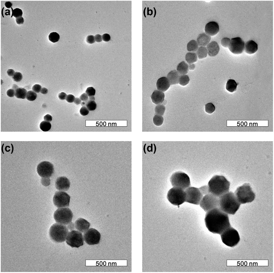 | ||
| Fig. 3 TEM images of CdTe SPs with the diameters from 80 to 330 nm. | ||
As mentioned earlier, the white light of WLEDs is generally produced by combining the blue exciting light from the InGaN/GaN chip and the green, red emitting lights from the color conversion materials. Since there is the overlap between PL emission spectra of green-emitting CdTe QDs/SPs and absorption spectra of red-emitting CdTe QDs/SPs, CdTe-PVA composite films containing both green- and red-emitting CdTe QDs/SPs are fabricated as the research platform for studying their inter-QD/SP FRET.34,35 In a typical fabrication process, a constant weight of green-emitting CdTe QDs/SPs (10 wt% compared to PVA) mixed with different weights of red-emitting CdTe QDs/SPs are blended in the PVA aqueous solution, followed by spin-coating on a 1 × 1 cm hydroxylated quartz plate and vacuuming to remove any residual solvent. From the TEM image of the composite film, it can be seen that CdTe SPs are monodispersed in PVA without any aggregation and breakage (Fig. S4†). Then, PL emission spectra are used to monitor the fluorescence of CdTe-PVA films comprising double colored (green and red) CdTe QDs/SPs. As shown in Fig. 4a, the pure green-emitting CdTe SP-PVA film exhibits a single emission peak at 522 nm. With increasing the concentration of red-emitting CdTe SPs (from 0 wt% to 8 wt% compared to PVA) in the film, the red emission peak at 640 nm appears and increases significantly, accompanied by a slightly decrease in the PL emission intensity of green-emitting CdTe SPs. The corresponding fluorescent lifetimes of the CdTe SP-PVA films are further characterized. As shown in Fig. 4c and e, the CdTe SP-PVA film comprising pure green-emitting CdTe SPs exhibits an average lifetime of 12.18 ns. The addition of red-emitting CdTe SPs do not have notable effect on its fluorescent lifetime. Even increasing the concentration of red-emitting CdTe SPs to 8 wt% (compared to PVA), only negligible variation on the fluorescent lifetimes of the CdTe SP-PVA films can be found. As a comparison, the intensity of red emission gradually increases, but the green emission quench dramatically when increasing the concentration of red-emitting CdTe QDs in the CdTe QD-PVA films (Fig. 4b). Accordingly, the fluorescent lifetimes of CdTe QD-PVA films are getting shorter and shorter (from 16.40 to 11.85 ns) upon the addition of red-emitting CdTe QDs (Fig. 4d and f).
 | ||
| Fig. 4 PL emission spectra (a), luminescence decay curves (c), and fluorescent lifetimes (e) of CdTe SP-PVA films containing different concentration of green- and red-emitting CdTe SPs. PL emission spectra (b), luminescence decay curves (d), and fluorescent lifetimes (f) of CdTe QD-PVA films containing different concentration of green- and red-emitting CdTe QDs. | ||
By integrating the results of the PL emission spectra and the fluorescent lifetimes, an appropriate mechanism is proposed to describe the FRET process between SPs and QDs. Since the SP structures possess the submicron size, which can significantly enlarge the distance between QDs with different emissions. The inter-SP FRET can be efficiently blocked. In contrast, directly mixing QDs with different emissions can easily induce the inter-QD distance smaller than 10 nm during their aggregation. As a result, the presence of red-emitting CdTe QDs work as the additional decay channels to accelerate the exciton recombination in green-emitting CdTe QDs, leading to the decrease of their fluorescence lifetime accompanied by the energy transfer from high-energy QDs to low-energy QDs. It is note that the fluorescent lifetime of CdTe SP-PVA film is almost independent of red-emitting CdTe SPs' concentration, thus the slight decrease of the green emission upon the addition of red-emitting CdTe SPs may derive from the paltry reabsorption by red-emitting CdTe SPs.
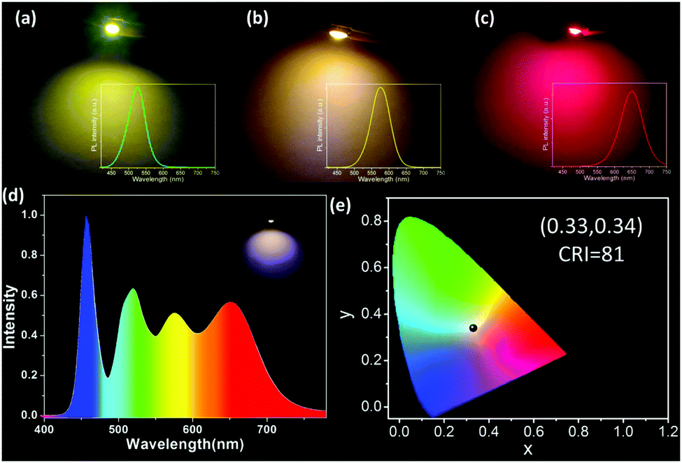
In order to verify our mechanism, the single-color and triple-color CdTe-PVA films by incorporating individual green-, yellow-, and red-emitting CdTe SPs/QDs and their mixture with the same concentration are fabricated. Fig. 5a exhibits the PL emission spectra of green-, yellow-, and red-color CdTe SP-PVA films, the overlap of their PL emission spectra, and the practical PL emission spectrum of the triple-color CdTe SP-PVA film. From which it can be seen that by using CdTe SPs as the color conversion materials, the ratio of fluorescence intensity between green, yellow, and red emissions in the overlapped spectrum is closely approximate to that in the practical spectrum of the triple-color CdTe SP-PVA film. However, a distinct enhancement in red emission along with the red-shift of the green and yellow emissions can be found in the PL emission spectrum of the triple-color CdTe QD-PVA film comparing with the overlapped spectrum (Fig. 5b). Thus, it is reasonable to believe that CdTe SPs, which can efficiently alleviate the FRET between CdTe with different emissions, are ideal color conversion materials for fabricating WLEDs with predictable PL emission spectra. At last, CdTe SPs with the emission centered at 520, 565, and 645 nm are prepared and blended with PVA individually, then coated on a commercially available 365 nm GaN LED chip to produce monochromatic LEDs. Fig. 6a–c exhibit the photographs of these working monochromatic LEDs. They all exhibit high brightness and relatively pure emission color. Subsequently, by mixing green-, yellow-, and red-emitting CdTe SPs in a certain ratio, the WLED possessing emissions matching perfectly with the theory PL spectrum are fabricated (Scheme 1b and Fig. 6d). And the luminous efficacy of the as-prepared WLED is 27 lm W−1. Accordingly, the color coordinate, color temperature, and CRI are (0.33, 0.34), 5742 K, and 81% respectively. As a comparison, following the same fabrication process but using CdTe QDs instead of CdTe SPs as the color conversion materials, the resulting LED device exhibits obvious deviations between its theoretic and practical PL spectra and color coordinates (Fig. S5†).
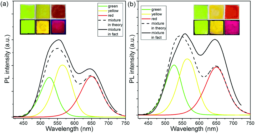 | ||
| Fig. 5 (a) PL emission spectra of green-, yellow-, and red-color CdTe SP-PVA films, the overlap of their PL emission spectra, and the PL emission spectrum of the triple-color CdTe SP-PVA film. (b) PL emission spectra of green-, yellow-, and red-color CdTe QD-PVA films, the overlap of their PL emission spectra, and the PL emission spectrum of the triple-color CdTe QD-PVA film. Insets: photographs of single-color CdTe SP-PVA films and CdTe QD-PVA films under sunlight (top) and UV irradiation (down). | ||
 | ||
| Fig. 6 (a–c) Photographs of the working monochromatic LEDs. PL emission spectrum (d) and CIE (e) of the WLED fabricated by mixing green-, yellow-, and red-emitting CdTe SPs in a certain ratio. | ||
Conclusion
In conclusion, we present a straightforward method for the fabrication of WLEDs without FRET by using CdTe SPs as the color conversion materials. The CdTe SPs are assembled by CdTe QDs via a two-step phase transfer strategy. Comparing with individual CdTe QDs, CdTe SPs possess submicron size, which efficiently eliminate the FRET process by enlarging the distance between QDs with different emissions. In contrast, directly mixing CdTe QDs instead of SPs will lead to an obvious red-shift derived from FRET due to their nanoscale size and small inter-QD distance. What is important, by easily overlapping the individual fluorescence spectra of CdTe SPs with different emissions, the certain ratio of their usage for fabricating LEDs with desired PL emission spectra can be identified. According to this idea, a WLED with CRI of 81, luminous efficacy of 27 lm W−1, and color coordinate at (0.33, 0.34) with the color temperature of 5742 K is achieved. Since the influence of FRET on the fluorescence emission of LEDs is irregular, our strategy may open a way for realizing the fabrication of LEDs with predictable PL emission spectra.Conflicts of interest
There are no conflicts to declare.Acknowledgements
This work was supported by the National key research and development program of China (2016YFB0401701), NSFC (No. 21875086).Notes and references
- D. Irvine-Halliday, R. Peon, G. Doluweera, I. Platonova and G. Irvine-Halliday, SPIE Newsroom, 2006, 10, 0056 Search PubMed.
- Q. Dai, C. E. Duty and M. Z. Hu, Small, 2010, 6, 1577–1588 CrossRef CAS PubMed.
- S. Reineke, Nat. Mater., 2015, 14, 459–462 CrossRef CAS.
- F. Yuan, Z. Wang, X. Li, Y. Li, Z. A. Tan, L. Fan and S. Yang, Adv. Mater., 2017, 29, 1604436 CrossRef.
- V. Fernández-Luna, P. B. Coto and R. D. Costa, Angew. Chem., Int. Ed., 2018, 57, 8826–8836 CrossRef.
- X. Wang, X. Yan, W. Li and K. Sun, Adv. Mater., 2012, 24, 2742–2747 CrossRef CAS.
- T. Erdem and H. V. Demir, Nanophotonics, 2013, 2, 57–81 CAS.
- N. H. Kim, J. Jeong and H. Chae, Appl. Sci. Converg. Technol., 2016, 25, 1–6 CrossRef.
- H. V. Demir, S. Nizamoglu, T. Erdem, E. Mutlugun, N. Gaponik and A. Eychmüller, Nano Today, 2011, 6, 632–647 CrossRef CAS.
- Y. Kamiyama, T. Hiroshima, T. Isobe, T. Koizuka and S. Takashima, J. Electrochem. Soc., 2010, 157, J149–J154 CrossRef CAS.
- T. T. Xuan, J. Q. Liu, R. J. Xie, H. L. Li and Z. Sun, Chem. Mater., 2015, 27, 1187–1193 CrossRef CAS.
- X. Dai, Y. Deng, X. Peng and Y. Jin, Adv. Mater., 2017, 29, 1607022 CrossRef.
- F. Todescato, I. Fortunati, A. Minotto, R. Signorini, J. Jasieniak and R. Bozio, Materials, 2016, 672 CrossRef.
- J. Cho, J. H. Park, J. K. Kim and E. F. Schubert, Laser Photonics Rev., 2017, 11, 1600147 CrossRef.
- Y. Shirasaki, G. J. Supran, M. G. Bawendi and V. Bulović, Nat. Photonics, 2013, 7, 13 CrossRef CAS.
- B. Zhao, Y. Yao, M. Gao, K. Sun, J. Zhang and W. Li, Nanoscale, 2015, 7, 17231–17236 RSC.
- K. Chou and A. Dennis, Sensors, 2015, 15, 13288–13325 CrossRef.
- H. G. Hong, M. H. Shin, H. J. Kim, J. Shin and Y. J. Kim, J. Nanomater., 2015, 2015, 4 Search PubMed.
- S. Mayilo, J. Hilhorst, A. S. Susha, C. Höhl, T. Franzl, T. A. Klar and J. Feldmann, J. Phys. Chem. C, 2008, 112, 14589–14594 CrossRef CAS.
- O. V. Mikhnenko, P. W. Blom and T. Q. Nguyen, Energy Environ. Sci., 2015, 8, 1867–1888 RSC.
- B. Zhao, D. Zhang, K. Sun, X. Wang, R. Mao and W. Li, RSC Adv., 2014, 4, 45155–45158 RSC.
- Y. H. Won, H. S. Jang, K. W. Cho, Y. S. Song, D. Y. Jeon and H. K. Kwon, Opt. Lett., 2009, 34, 1–3 CrossRef CAS.
- M. Liu, W. Yao, C. Li, Z. Wu and L. Li, RSC Adv., 2015, 5, 628–634 RSC.
- M. Li, J. Zhang, H. Zhang, Y. Liu, C. Wang, X. Xu and B. Yang, Adv. Funct. Mater., 2007, 17, 3650–3656 CrossRef.
- C. J. Chen, C. C. Lin, J. Y. Lien, S. L. Wang and R. K. Chiang, J. Mater. Chem. C, 2015, 3, 196–203 RSC.
- H. Zhang, Y. Liu, J. Zhang, H. Sun, J. Wu and B. Yang, Langmuir, 2008, 24, 12730–12733 CrossRef CAS.
- T. Wang, D. LaMontagne, J. Lynch, J. Zhuang and Y. C. Cao, Chem. Soc. Rev., 2013, 42, 2804–2823 RSC.
- H. Zou, M. Liu, D. Zhou, X. Zhang, Y. Liu, B. Yang and H. Zhang, J. Phys. Chem. C, 2017, 121, 5313–5323 CrossRef CAS.
- X. Zhang, J. Han, T. Yao, J. Wu, H. Zhang, H. Zhang and B. Yang, CrystEngComm, 2011, 13, 5674–5676 RSC.
- J. E. Park, D. R. Hickey, S. Jun, S. Kang, X. Hu, X. J. Chen and S. J. Park, Adv. Funct. Mater., 2016, 26, 7791–7798 CrossRef CAS.
- X. Zhang, J. Han, T. Yao, J. Wu, H. Zhang, H. Zhang and B. Yang, CrystEngComm, 2011, 13, 5674–5676 RSC.
- S. Liu, L. Wang, M. Zhang, K. Tao, B. Wang, M. Lin, X. Zhang, Y. Liu, Y. Hou, H. Zhang and B. Yang, ACS Appl. Mater. Interfaces, 2019, 11, 25730–25739 CrossRef CAS.
- J. Han, X. Zhang, Y. Zhou, Y. Ning, J. Wu, S. Liang and B. Yang, J. Mater. Chem., 2012, 22, 2679–2686 RSC.
- M. Li, X. Xu, Y. Tang, Z. Guo, H. Zhang, H. Zhang and B. Yang, J. Colloid Interface Sci., 2010, 346, 330–336 CrossRef CAS.
- Y. Tang, H. Zhang, Z. Fan, M. Li, J. Han, F. Dong and B. Yang, Phys. Chem. Chem. Phys., 2010, 12, 11843–11849 RSC.
Footnote |
| † Electronic supplementary information (ESI) available: XRD patterns, SEM images, and PL emission spectra of CdTe NPs and SPs. Molar ratio of Cd/Te in CdTe NPs and SPs. See DOI: 10.1039/c9ra06254h |
| This journal is © The Royal Society of Chemistry 2019 |