DOI:
10.1039/C9RA06230K
(Paper)
RSC Adv., 2019,
9, 29993-29997
Enhanced photocurrent in organic photodetectors by the tunneling effect of a hafnium oxide thin film as an electron blocking layer†
Received
10th August 2019
, Accepted 18th September 2019
First published on 23rd September 2019
Abstract
To achieve high detectivity of organic photodetectors (OPDs), we investigated hafnium oxide (HfO2) as an electron blocking layer in an attempt to obtain a low leakage current and high photocurrent by the tunneling effect. The prepared devices consisted of indium tin oxide (ITO)/HfO2/(poly(3-hexylthiophene-2,5-diyl)[P3HT]:PC60BM)/Yb/Al. To explore the tunneling effect in a hafnium oxide thin film, we fabricated a thin film using successive ionic layer deposition. The results for hafnium oxide were compared with those for aluminum oxide and poly(3,4-ethylenedioxythiophene)poly(styrenesulfonate) (PEDOT:PSS). We found that hafnium oxide results in a low leakage current and high photocurrent owing to the tunneling effect in the OPDs. The resulting detectivity of 1.76 × 10¹² Jones for a film thickness of 5.5 nm and bandwidth of ∼100 kHz is suitable for commercialization.
Introduction
Photodetectors are used in a wide variety of applications to convert light into electrical signals, consumer electronics, mobile devices, vehicle systems, military applications, and security1–3 Most conventional photodetectors are based on inorganic materials such as silicon and group III–V compounds and have been developed due to their high charge-carrier mobility, small exciton binding energy and high stability.4 However, inorganic-based photodetectors have limitations for use in advanced applications because of complicated manufacturing processes and mechanical inflexibility,5 and the low visible-spectrum sensitivity of inorganic photodetectors makes them susceptible to noise owing to the absorption of infrared wavelengths. Despite this, inorganic photodetectors have many advantages, such as high photoelectric conversion efficiency and high detectivity.6,7 Currently, organic solution-processable photodetectors (OPDs) are considered advantageous because of their light weight, low cost, and flexibility, but their use remains hindered by poor leakage current and low detectivity.1,8
One of the most important parameters for OPD performance is detectivity, which is also affected by leakage current.9 The leakage current in OPDs has been improved by blocking electrons sourced from the external bias. The electrons are blocked by an interlayer composed of a high work function material, and holes are blocked by a cathode interlayer with a low work function.10,11 The electron blocking layers serve to block leakage current under a reverse bias and extract photo-generated carriers from the active layer to the electrode, whereas the hole blocking layer is supported by an external bias and reduced charge recombination in the active layer.12 For a p-type buffer layer, PEDOT:PSS [poly(3,4-ethylenedioxythiophene)poly(styrenesulfonate)] has been widely used as a hole transporting material. However, OPDs using a PEDOT:PSS layer contend with problems involving high dark current densities from leakage current and poor device stability.13 In this study, we introduced thin film of hafnium oxide as an electron blocking layer to reduce the dark current density caused by the leakage current and improved the on–off current ratio and detectivity. To understand and the effective thickness of hafnium oxide layer for low leakage current and tunneling effect, we applied successive ionic layer deposition (SILD)14,15 as hafnium thin film fabrication technique which can be deposited less than 4 nm thickness film. Hafnium oxide has a high bandgap (5.0–6.0 eV) and can control leakage currents, making it widely used as an insulator in semiconductor industries.16,17 In addition, hafnium oxide is an effective material for blocking carriers owing to its characteristics as an insulator. In a ∼5 nm thin film, tunneling can happen in certain device configurations18,19 and has been shown to occur in OPD devices.
Herein, we demonstrate OPDs with high detectivity using hafnium oxide in an ITO/HfO2/P3HT:PC60BM/Yb/Al configuration. To fabricate hafnium oxide thin films, 2.0 nm, 5.5 nm and 11 nm layer of hafnium oxide was deposited by SILD.14,15 Hafnium oxide, PEDOT:PSS, and aluminum oxide were compared as electron blocking layers to understand and analyze the reason for the low dark current and the effect of tunneling in the OPD device by selection of similar energy level metal oxides, and ytterbium was used as the electron transport layer for a high photocurrent.20 Using the hafnium oxide in the OPD devices as an electron blocking layer, we found that the hafnium oxide thin film in the OPD device controls the dark current by blocking external bias under a wide bandgap and high lowest unoccupied molecular orbital (LUMO) level in the dark state; furthermore, it enhances the photocurrent by way of the tunneling effect in the light state, as confirmed by comparison with aluminum oxide, which has a similar wide band gap and LUMO level.
Experimental
Materials and reagents
Hafnium(IV) chloride, poly(3-hexylthiophene-2,5-diyl) (P3HT) was purchased from Sigma-Aldrich Co., Ltd. [6,6]-Phenyl-C61-butyricacidmethylester (PC60BM) was obtained from Nano-C. Poly(3,4-ethylenedioxythiophene):poly(styrenesulfonate) (PEDOT:PSS, Clevious Al 4083) was purchased from Heraeus. Ytterbium and aluminum were purchased from ITASCO. The other chemicals used were of reagent grade.
Fabrication of organic photodetectors (OPDs)
Patterned ITO (≤20 ohm sq−1) glass substrates were cleaned in an ultrasonic bath of acetone, isopropyl alcohol and deionized water for 15 minutes for each solvent, then by UV/ozone treatment for 15 minutes. HfO2 thin films were deposited on patterned ITO glass substrates which the above cleaning sequence. The hafnium oxide deposition was carried out by a successive ionic layer deposition (SILD)14,15 method. The cationic precursor solution used was 0.01 M hafnium chloride (hafnium(IV) chloride) in 2-methoxy ethanol and the pH was controlled by sodium hydroxide. The anionic precursor solution used 1 vol% hydroperoxide solution in DI-water. The deposition of HfO2 thin film takes place as described below.
In the first step, well-cleaned patterned ITO glass substrate was immersed for 20 seconds in the cationic precursor solution of hafnium chloride. The hafnium ions get adsorbed to the surface of the substrate. Afterwards, the substrate was rinsed for 20 seconds by DI-water to remove excessively adsorbed ions.
In the second step, the substrate was immersed for 20 seconds in the anionic precursor solution of hydroperoxide. The hydroxide ions react with adsorbed hafnium ions on the substrate to form HfO−. The substrate was rinsed for 20 seconds by DI-water to remove excessive substrate again.
The above two steps together constitute one complete cycle of deposition. This cycle was repeated several times to get well adhesiveness and homogeneous HfO2 thin layers. Finally, annealed at 400 °C for 30 minutes in a furnace for the perfect oxidation of HfO2 thin film. OPD devices consisting of ITO (200 nm)/HfO2/P3HT:PC60BM (210 nm)/Yb (2 nm)/Al (100 nm) were fabricated on the hafnium oxide thin film deposited ITO glass. The device was transferred into a nitrogen filled glove box where a solution of P3HT![[thin space (1/6-em)]](https://www.rsc.org/images/entities/char_2009.gif) :PC60BM (1:1) in dichlorobenzene (36 mg ml−1) was spin-cast at 900 rpm onto the hafnium oxide thin film and annealed at 120 °C for 10 minutes on a hot plate. Finally, ytterbium and aluminum were deposited by using a thermal evaporation technique at 10−6 torr (ULVAC VTR-300M/1ERH evaporator, Japan).
:PC60BM (1:1) in dichlorobenzene (36 mg ml−1) was spin-cast at 900 rpm onto the hafnium oxide thin film and annealed at 120 °C for 10 minutes on a hot plate. Finally, ytterbium and aluminum were deposited by using a thermal evaporation technique at 10−6 torr (ULVAC VTR-300M/1ERH evaporator, Japan).
Device characteristics
Current–voltage measurements were performed under simulated AM 1.5 solar illumination (at 100 mW cm−2) using a solar simulator (Newport 69920, Newport Co., Ltd, USA) with 525 nm color filter and IVUMSTAT (SpectraPro300i, Acton Research Co., Ltd, USA). The work function and film thickness were measured using an ultraviolet photoelectron spectroscope (Thermo Fisher Scientific Co., Ltd, USA) and Spectroscopic Ellipsometer (Woollam Co.). Bandwidth were obtained using a photo response measurement system (TNE Tech Co., Ltd, South Korea).
Results and discussion
Tunneling effect with hafnium oxide thin film OPD devices
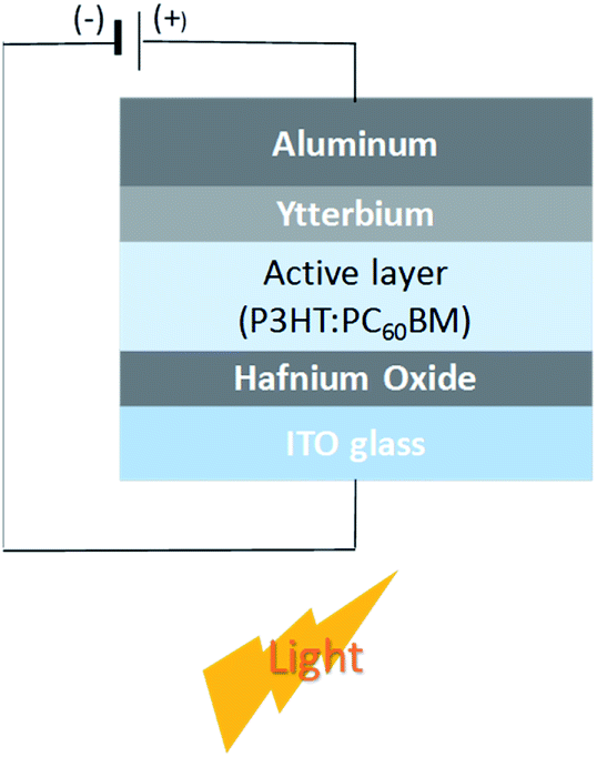
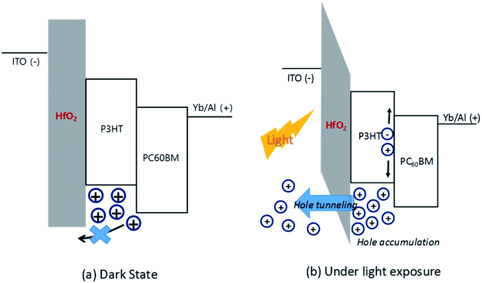
Fig. 1 shows the configuration of the OPD with hafnium oxide as the electron blocking layer and ytterbium as the electron transfer interlayer. The energy band diagram of the OPD is shown in Fig. 2 in a dark state and under light exposure. A thin film of a wide band gap hafnium oxide was fabricated as an electron blocking material on an ITO electrode, and the use of ytterbium effectively supported electron transfer to the electrode.20 OPD performance depends on blocking the leakage current electrons and a high photocurrent to achieve high detectivity. As shown in Fig. 2, photocurrent density was enhanced by the tunneling effect of hafnium oxide under light exposure owing to energy band bending, which is induced by hole accumulation,18 and the leakage current from external bias was blocked by the high LUMO level of hafnium oxide.
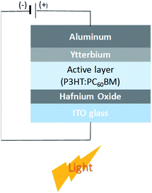 |
| | Fig. 1 Device structure of the prepared organic photodetector device (OPD). | |
 |
| | Fig. 2 Tunneling effect of organic photodetector device (OPD) with a hafnium oxide thin film. | |
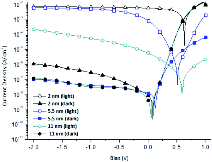
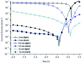
Table 1 and Fig. 3 show the current density–voltage characteristics of the OPDs with different hafnium oxide thin film thicknesses as the electron blocking layer. The photocurrent and dark current density decreased proportionally to the thickness of the hafnium oxide film, confirming that a high hafnium oxide LUMO level can act as a high energy barrier between the ITO electrode and active layer.
Table 1 Organic photodetector device (OPD) performance using different thicknesses of a hafnium oxide interlayer at −1 V
| Thickness (nm) |
Hafnium wt% (FE-SEM) |
Photocurrent density (A cm−2) |
Dark current density (A cm−2) |
On–off current ratio |
| 2.0 |
0.47 |
6.97 × 10⁻³ |
3.02 × 10⁻⁷ |
2.31 × 10⁴ |
| 5.5 |
1.04 |
5.27 × 10⁻³ |
4.15 × 10⁻⁸ |
1.27 × 10⁵ |
| 11 |
4.06 |
5.66 × 10⁻⁵ |
3.31 × 10⁻⁸ |
1.71 × 10³ |
 |
| | Fig. 3 Current density–voltage curves of organic photodetector devices (OPDs) with various hafnium oxide electron blocking layer thicknesses. | |
We found that at a thickness of 5.5 nm, electrons passed through the hafnium oxide thin film, and its electron blocking effect decreased dramatically. Photocurrent density and dark current density tended to be inversely proportional to hafnium oxide thickness. However, when the thickness was 5.5 nm, accumulated holes in the active layer owing to the HOMO level of hafnium oxide caused energy band bending, leading to quantum tunneling and extraction of holes to the ITO electrode.18 The highest on–off current ratio of 1.27 × 10⁵ was observed for the OPD with 5.5 nm of hafnium oxide.
Analysis of OPDs using the hafnium oxide interlayer
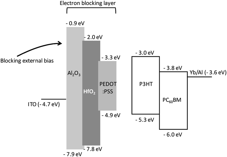
The energy band diagram of the OPDs is shown in Fig. 4. Two wide band gap metal oxides, hafnium oxide and aluminum oxide, and PEDOT:PSS were compared as electron blocking materials; wide band gap metal oxides are commonly used to enhance electron blocking under a reverse bias.21,22 In the OPD structure, the leakage current was blocked by the energy levels of the metal oxide materials, whereas the energy level of PEDOT:PSS allowed for easy electron movement by external bias.
 |
| | Fig. 4 Energy diagram of organic photodetector devices (OPDs) with three different electron blocking layers. | |
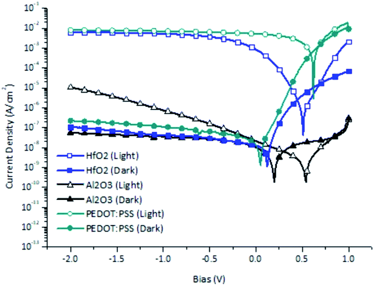
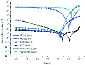
The current density–voltage characteristics of the prepared OPDs with different electron blocking layers are presented in Table 2 and Fig. 5. Their dark current densities were 4.15 × 10⁻⁸ A cm−2 at 5.5 nm of hafnium oxide, 3.53 × 10⁻⁸ A cm−2 at 6.0 nm of aluminum oxide, and 1.11 × 10⁻⁷ A cm−2 at 30 nm of PEDOT:PSS. The dark current density was reduced by the prevention of electron injection from the ITO electrode by the hafnium oxide thin layer. On the other hand, hafnium oxide at a certain thickness can transfer the photo-generated carriers produced by tunneling effects from the active layer. Thus, it can be argued that a hafnium oxide thin layer can behave as a hole transport material owing to the tunneling effect.
Table 2 Organic photodetector device (OPD) physical properties with three different electron blocking layer materials
| Material |
Thickness (nm) |
Photo current density (A cm−2) |
Dark current density (A cm−2) |
On–off current ratio |
Detectivity (Jones, at 520 nm) |
| HfO2 |
5.5 |
5.27 × 10⁻³ |
4.15 × 10⁻⁸ |
1.27 × 10⁵ |
1.76 × 10¹² |
| Al2O3 |
6.0 |
7.51 × 10⁻⁷ |
3.53 × 10⁻⁸ |
2.13 × 101 |
9.16 × 10¹⁰ |
| PEDOT:PSS |
30 |
8.26 × 10⁻³ |
5.00 × 10⁻⁶ |
1.60 × 10³ |
2.01 × 10¹¹ |
 |
| | Fig. 5 Current–voltage curves of organic photodetector devices (OPDs) with different electron blocking layer materials. | |
However, the HOMO–LUMO levels of hafnium oxide and aluminum oxide are similar, and their current density–voltage characteristics in our OPD configurations under a reverse bias were dissimilar. It seems that tunneling could happen in film thicknesses of 5.5 nm and 3 nm for hafnium oxide and aluminum oxide, respectively (see Table S1†). As shown in Table 1, 5.5 nm is the optimized hafnium oxide thickness for a low dark current and high photocurrent. In contrast, for aluminum oxide, the tunneling effect would occur in a thinner film, and the increase in photocurrent density would thus be limited in terms of significantly increasing the on–off ratio. However, aluminum oxide showed a comparably low photocurrent density in the OPD configuration owing to its relatively low capacitance,23 and thus it exhibited low charge accumulation and tunneling in the OPD configuration.
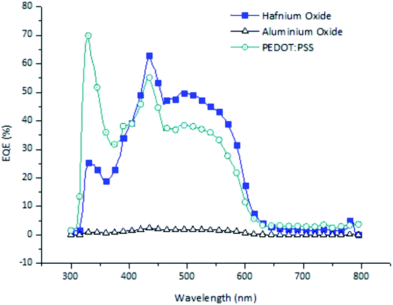
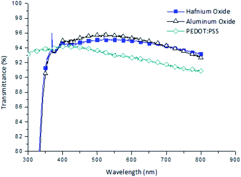
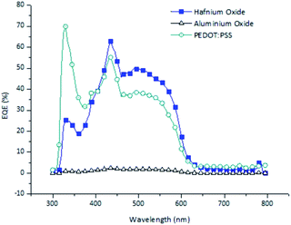
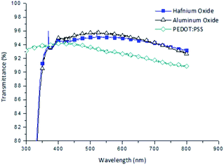
Fig. 6 shows the external quantum efficiencies (EQEs) at different wavelengths under reverse bias conditions at −1 V of the optimized OPDs using hafnium oxide, aluminum oxide, and PEDOT:PSS as electron blocking layers. All the OPDs showed photo-responses from 300 to 800 nm. At wavelengths of 300–400 nm, the EQE of the OPD using PEDOT:PSS was higher than that of the metal oxide based devices. In particular, the EQE of the hafnium oxide based OPD was higher than that of the PEDOT:PSS OPD at 400–600 nm, which was attributed to the high transmittance. The aluminum oxide based OPD showed very low EQEs over the whole range of wavelengths because the generated holes in the photoactive layer could not be effectively extracted to the electrode. High transmittance of hafnium oxide was expected in the visible range as the absorption was insignificant for wavelengths above 250 nm.24 The higher transmittance of hafnium oxide can detect light effectively in the visible rage, it is presented in the Fig. 7.
 |
| | Fig. 6 External quantum efficiencies (EQEs) of different organic photodetector devices (OPDs) with different electron blocking layer materials. | |
 |
| | Fig. 7 Transmittance of the electron blocking layers at various wavelength at 300–800 nm. | |
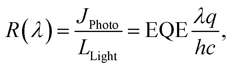
Responsivity (R), NEP (λ) and detectivity (D*) are the most important parameters in terms of OPD performance and can be calculated given the EQE. The detectivity is related to the responsibility and noise-equivalent power (NEP). The reciprocal of the NEP (Noise-Equivalent Power) is referred to as the detectivity of the device:20
| |
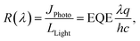 | (1) |
| |
 | (2) |
| |
 | (3) |
where
Llight is the incident light intensity,
λ is the wavelength,
q is the electron charge,
h is Planck's constant, and
c is the velocity of light in a vacuum,
IN is the total noise current and Δ
f is the bandwidth (Hz). At a wavelength of 520 nm, the responsivities of the OPDs using hafnium oxide, aluminum oxide, and PEDOT:PSS were 214, 8.2, and 166 mA W
−1, respectively, under reverse bias conditions at −1 V. The high responsivity and low dark current density of the hafnium oxide OPD improved its detectivity (1.76 × 10
12 Jones at 520 nm). This detectivity was two times higher than that of the OPD using a PEDOT:PSS buffer layer (9.16 × 10
11 Jones) and 10 times higher than that of the aluminum oxide OPD (1.23 × 10
11 Jones).
Transient photocurrent response characteristics
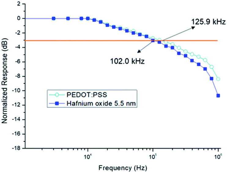
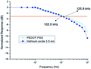
The frequency responses of the OPDs were analyzed under reverse bias conditions at −1 V by measuring the frequency at −3 dB. Fig. 8 shows the frequency responses of the OPDs with two different electron blocking layers. The value of 102.0 kHz for the hafnium oxide OPD is comparable to that of the well-known PEDOT:PSS OPD material, 125.9 kHz, indicating its potential for commercialization. The photoreaction of the photodetector tends to attenuate as the frequency of the optical signal increases. Typically, the −3 dB bandwidth of the photodetector device is determined by the frequency at which the response output attenuates to −3 dB.25
 |
| | Fig. 8 Frequency responses of optimized organic photodetector devices (OPDs) using hafnium oxide and poly(3,4-ethylenedioxythiophene)poly(styrenesulfonate) (PEDOT:PSS) interlayers at −1 V. | |
Conclusions
We fabricated OPDs using hafnium oxide, a known insulator, as a blocking layer with a tunneling effect. We found that because of its tunneling effect, a 5.5 nm-thick hafnium oxide film can be used as a blocking layer in photodetectors. The optimized devices with hafnium oxide interlayers showed better performance than devices with PEDOT:PSS and aluminum oxide. The photocurrent of the OPDs reached 5.27 × 10⁻³ A cm−2 and an on–off current ratio of 1.27 × 10⁵ was measured under reverse bias conditions at −1 V. Additionally, we observed a detectivity of 1.76 × 10¹² Jones for our device at 525 nm under reverse bias conditions at −1 V and a bandwidth of 102.0 kHz, which is comparable to that of PEDOT:PSS (125.9 kHz). Therefore, we successfully produced a thin hafnium oxide film to improve the performance of OPDs using the basic fabrication technique of SILD onto ITO.
Conflicts of interest
There are no conflicts to declare.
Acknowledgements
This research was supported by Basic Science Research Program through the National Research Foundation of Korea (NRF) funded by the Ministry of Education (NRF-2017R1D1A1B03028795). This study was supported by “Human Resources Program in Energy Technology” of the Korea Institute of Energy Technology Evaluation and Planning (KETEP), granted financial resource from the Ministry of Trade, Industry & Energy, Republic of Korea (No. 20174010201150).
Notes and references
- P. Peumans, V. Bulovic and S. R. Forrest, Appl. Phys. Lett., 2000, 76, 3855 CrossRef CAS
 .
. - D. Yang and D. Ma, Adv. Opt. Mater., 2019, 7, 1800522 CrossRef .
- F. Teng, K. Hu, W. Ouyang and X. Fang, Adv. Mater., 2018, 30, 1706262 CrossRef PubMed .
- R. Vuuren, A. Armin, A. Pandey, P. Burn and P. Meredith, Adv. Mater., 2016, 28, 4766 CrossRef PubMed .
- F. Arquer, A. Armin and P. Meredith, Nat. Rev. Mater., 2017, 2, 16100 CrossRef .
- K.-J. Baeg, M. Binda, D. Natali, M. Caironi and Y.-Y. Noh, Adv. Mater., 2003, 25, 4267 CrossRef PubMed .
- G. Konstantatos, J. Clifford, L. Levina and E. H. Sargent, Nat. Photonics, 2007, 1, 531 CrossRef CAS .
- P. E. Keivanidis, S.-H. Khong, P. K. H. Ho, N. C. Greenham and R. H. Friend, Appl. Phys. Lett., 2009, 94, 173303 CrossRef .
- G. Konstantatos and E. H. Sargent, Nat. Nanotechnol., 2010, 5, 391 CrossRef CAS PubMed .
- M. T. Greiner, M. G. Helander, W.-M. Tang, Z.-B. Wang, J. Qiu and Z.-H. Lu, Nat. Mater., 2012, 11, 76 CrossRef CAS PubMed .
- V. Gupta, A. K. K. Kyaw, D.-H. Wang, S. Chand, G. C. Bazan and A. J. Heeger, Sci. Rep., 2013, 3, 1965 CrossRef PubMed .
- S. Lattante, Electronics, 2014, 3, 132 CrossRef CAS .
- P. Schilinsky and C. Waldauf, Appl. Phys. Lett., 2002, 81, 3885 CrossRef CAS .
- R. L. Puurunen, J. Appl. Phys., 2005, 97, 121301 CrossRef .
- İ. A. Kariper, Int. J. Miner., Metall. Mater., 2014, 21, 832 Search PubMed .
- Y. B. Yoo, J. H. Park, K. H. Lee, H. W. Lee, K. M. Song, S. J. Lee and H. K. Baik, J. Mater. Chem. C, 2013, 1, 1651 RSC .
- X. Zhao, Phys. Rev. B, 2002, 65, 233106 CrossRef .
- G. Shoute, A. Afshar, T. Muneshwar, K. Cadien and D. Barlage, Nat. Commun., 2016, 7, 10632 CrossRef CAS PubMed .
- J. J. Lee, X. Wang, W. Bai, N. Lu and D. L. Kwong, IEEE Trans. Electron Devices, 2003, 50, 2067 CrossRef CAS .
- S. B. Lim, C. H. Ji, I. S. Oh and S. Y. Oh, J. Mater. Chem. C, 2016, 4, 4920 RSC .
- M. Vogel, S. Doka, C. Breyer, M. C. Lux-Steiner and K. Fostiropoulos, Appl. Phys. Lett., 2006, 89, 163501 CrossRef .
- J. R. Manders, T.-H. Lai, Y. An, W. Xu, J.-W. Lee, D.-Y. Kim, G. Bosman and F. So, Adv. Funct. Mater., 2014, 24, 7205 CAS .
- J. Robertson, Eur. Phys. J.: Appl. Phys., 2004, 28(3), 265 CrossRef CAS .
- M. F. Al-Kuhaili, Opt. Mater., 2004, 27(3), 383 CrossRef CAS .
- B. O. Arredondo, B. Romero, C. de Dios, R. Vergaz, R. Criado and J.-M. Sanchez-Pena, Spanish Conference on Electron Devices, Valladolid, Spain, 2013, Feb 12–14 Search PubMed .
Footnote |
| † Electronic supplementary information (ESI) available. See DOI: 10.1039/c9ra06230k |
|
| This journal is © The Royal Society of Chemistry 2019 |
Click here to see how this site uses Cookies. View our privacy policy here. 
 Open Access Article
 This Open Access Article is licensed under a Creative Commons Attribution-Non Commercial 3.0 Unported Licence
 *
*