DOI:
10.1039/C9RA06132K
(Paper)
RSC Adv., 2019,
9, 42415-42422
Thermal effect of annealing-temperature on solution-processed high-k ZrO2 dielectrics†
Received
7th August 2019
, Accepted 4th December 2019
First published on 20th December 2019
Abstract
In this paper, a solution-processed zirconium oxide (ZrO2) dielectric was deposited by spin coating with varying pre-annealing temperatures and post-annealing temperatures. The thermal effect of the pre-annealing and post-annealing process on the structural and electrical properties of ZrO2 films was investigated. The result shows that the pre-annealing process had a significant impact on the relative porosity and internal stress of ZrO2 film. A pre-annealing process with a low temperature could not effectively remove the residual solvent, while a high pre-annealing temperature would lead to large internal stress. As for post-annealing temperature, it was found that the post-annealing process can not only reduce internal defects of the ZrO2 dielectric, but also optimize the interface between the semiconductor and dielectric by lowering the surface defects of the ZrO2 film. Finally, the TFT with a pre-annealing temperature of 200 °C and post-annealing temperature of 400 °C showed optimized performance, with a mobility of 16.34 cm2 (V s)−1, an Ion/Ioff of 2.08 × 10⁶, and a subthreshold swing (SS) of 0.17 V dec−1.
1. Introduction
Nowadays, metal-oxide (MOx) thin film transistors (TFTs) have attracted widespread attention in many fields, such as flat panel displays (FPDs), because of their excellent electrical performance, high transparency, good uniformity and compatibility with a variety of preparation processes.1–4 One of the most important parts in thin film transistors is the dielectric layer, which can insulate the semiconductor from the gate electrode, so that the carriers can be controllably aggregated in a semiconductor. Recently, research on metal-oxide dielectrics with high dielectric constants (high-k) (e.g., ZrO2,5 Al2O3,6 HfO2 (ref. 7) and Y2O3 (ref. 8)) has been widely carried out, and some researchers have explored the application of metal oxide dielectrics in TFT devices. ZrO2 has a high dielectric constant (∼25), high melting point (4300 °C), high refractive index and wide bandgap (∼6 eV).9,10 Due to these excellent physical properties, ZrO2 has been regarded as one of the ideal metal-oxide dielectrics with low leakage current density.
Solution phase method (e.g., inkjet printing, spray coating and spin coating) is considered to be a novel approach to manufacturing high-quality MOx films with low cost, and in this paper ZrO2 films were fabricated by spin coating under ambient conditions. Thermal annealing, with the intention of removing impurities and decreasing the concentration of defect states, is regarded as a necessary process for high quality solution-processed films. Usually, the spin coating process is repeated several times to achieve the desired thickness and reduce pores and defects. After each spin coating, the wet film is briefly annealed, which is called pre-annealing process. And then, after deposition of the final layer, multi-layer films are annealed for a longer time, which is defined as post-annealing. Pre-annealing temperature is lower aiming to evaporating the solvent, while the higher post-annealing temperature plays an important role in promoting metal-oxide bond formation and reducing impurity.11 Several studies have been carried out to investigate the effect of thermal annealing on metal oxide film.12–14 However, the effect of pre-annealing temperature and post-annealing temperature was not systematically discussed in these reports. The pre-annealing process and post-annealing process can be associated with different reactions, and therefore a targeted, systematic analysis of their effects should be performed. In this paper, ZrO2 dielectrics were deposited by solution method with varying pre-annealing temperatures and post-annealing temperatures. The thermal effect of pre-annealing and post-annealing process on the structural and electrical properties of ZrO2 film was investigated. In particular, the effect of pre-annealing temperature on solvent evaporation and internal stress was discussed, while the effect of post-annealing temperature on the internal impurities and interface defects was also evaluated.
2. Results and discussion
Usually, a sol–gel process consists of two steps, hydrolysis and condensation.11,15 In order to explore the hydrolysis and condensation process, and choose the annealing temperature, the thermal gravimetric and differential scanning calorimetry (TGA-DSC) analysis was carried out. Fig. 1(a) is the TG-DSC result of ZrO2 precursor. The endothermic reactions at 99.7 °C and 136.5 °C indicated hydrolysis of the ZrO2 solution and solvent evaporation. There was no significant weight change after 150 °C, corresponding to the boiling point of the 2-MOE solvent. The exothermic peak at 155.0 °C indicated the formation of metal–oxygen–metal (M–O–M) framework. The endothermic peak at 175.5 °C was associated with the reduction of impurities, while the exothermic peaks (at 335.6, 443.5 and 671.6 °C) can be attributed to the crystallization.
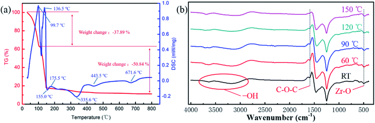 |
| | Fig. 1 (a) The TG-DSC result of ZrO2 precursor at a heating rate of 10 °C min−1. (b) The FTIR spectra of ZrO2 precursor annealed at different temperatures. | |
To further analyse the thermal behaviour of ZrO2 precursor, the Fourier Transform Infrared (FTIR) analysis was carried out with ZrO2 precursor annealed at different temperatures (room temperature (RT), 60, 90, 120 and 150 °C). As shown in Fig. 1(b), the absorption peak located at 3000–3800 cm−1 represents the stretching vibration of –OH bonding, which was derived from the absorption of oxygen in the air to form an –OH group. The peak located at 1600 cm−1 can be associated with the C–O–C group, which was mainly derived from the residual solvent. It can be seen that when the annealing temperature reached 150 °C, no C–O–C group was detected, indicating that the solvent was substantially removed. The absorption peak at 1470–1360 cm−1 and 1250–1030 cm−1 were caused by the bending vibration of carbon–hydrogen bond and bending vibration of carbon–oxygen bond, respectively. Finally, the absorption peak at 500 cm−1 can be attributed to the Zr–O group.
Based on the discussion above, an annealing temperature higher than 136 °C is necessary for the removal of solvent, while above 155 °C is important for promoting metal-oxide bond formation. In addition, a crystalline ZrO2 film can be obtained with an annealing temperature higher than 350 °C. In order to investigate the effect of pre-annealing temperature and post-annealing temperature on the properties of ZrO2 films, a series of experiments were carried out.
2.1 The effect of pre-annealing temperature
The ZrO2 film was deposited by spin-coating at 5000 rpm for 40 s and the spin-coating process was repeated 3 times. The pre-annealing temperature was set to 100, 200, 300 and 400 °C (for 5 min), and the post-annealing temperature was set to 450 °C. These films were labelled as 100-Zr, 200-Zr, 300-Zr and 400-Zr, respectively. A high post-annealing temperature could facilitate crystallization, which is advantageous for analysing the internal stress of ZrO2 films. The thickness and density of ZrO2 films with different pre-annealing temperatures were measured by XRR, as shown in Fig. 2(a). Based on the measured density, the relative porosity volume (R) of ZrO2 film was calculated by the following formula.16| |
 | (1) |
ρ1 and ρ represent the theoretical density of bulk ZrO2 materials (5.68 g cm−3) and the film density measured by XRR, respectively. ρh is the hole density (air), and in this case it is approximately zero. The detailed data of XRR result is listed in Table 1.
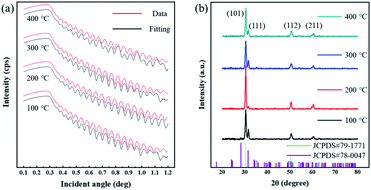 |
| | Fig. 2 (a) The XRR result of ZrO2 films with different pre-annealing temperatures. (b) XRD spectra the ZrO2 films at different pre-annealing temperatures. | |
Table 1 Structural parameters of ZrO2 films with different pre-annealing temperature
| Sample name |
Thickness (nm) |
Density (g cm−3) |
Relative porosity volume (%) |
hkl |
2θ (deg) |
FWHM (deg) |
d (Å) |
D (nm) |
ε (%) |
Average D (nm) |
Average ε (%) |
| 100-Zr |
84.37 |
5.12 |
9.93 |
101 |
30.39 |
0.41 |
2.94 |
19.70 |
0.33 |
19.79 |
0.25 |
| 111 |
31.57 |
0.35 |
2.83 |
23.05 |
0.27 |
| 112 |
50.53 |
0.41 |
1.81 |
21.02 |
0.19 |
| 211 |
60.33 |
0.59 |
1.53 |
15.39 |
0.22 |
| 200-Zr |
81.87 |
5.45 |
4.03 |
101 |
30.39 |
0.41 |
2.94 |
19.70 |
0.33 |
22.98 |
0.23 |
| 111 |
31.55 |
0.35 |
2.84 |
23.05 |
0.27 |
| 112 |
50.36 |
0.47 |
1.81 |
18.38 |
0.22 |
| 211 |
60.33 |
0.30 |
1.53 |
30.78 |
0.11 |
| 300-Zr |
84.47 |
5.20 |
8.45 |
101 |
30.41 |
0.41 |
2.94 |
19.70 |
0.33 |
18.65 |
0.27 |
| 111 |
31.62 |
0.47 |
2.83 |
17.29 |
0.36 |
| 112 |
50.44 |
0.47 |
1.81 |
18.39 |
0.22 |
| 211 |
60.38 |
0.47 |
1.53 |
19.24 |
0.18 |
| 400-Zr |
85.00 |
5.20 |
8.45 |
101 |
30.51 |
0.41 |
2.93 |
19.70 |
0.33 |
18.77 |
0.26 |
| 111 |
31.63 |
0.41 |
2.83 |
19.76 |
0.31 |
| 112 |
50.64 |
0.53 |
1.80 |
16.35 |
0.24 |
| 211 |
60.46 |
0.47 |
1.53 |
19.25 |
0.17 |
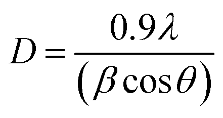
Fig. 2(b) is XRD spectra of ZrO2 films with different pre-annealing temperatures. All diffraction patterns shown characteristic ZrO2 peaks with both tetragonal structure and monoclinic structure [JCPDS#79-1771 and JCPDS#78-0047]. The diffraction peaks located at 30.3°, 50.4°, and 60.3° can be associated with (101), (112), and (211) crystal faces, respectively [tetragonal structure, JCPDS#79-1771]. The peak at 31.6° can be attributed to the (111) crystal face of ZrO2 with monoclinic structure [JCPDS#78-0047]. The Bragg's angle (2θ), full-width at half of the peak maximum (FWHM) and interplanar distance (d) of each crystal faces are listed in Table 1. Based on the above parameters, the average grain size (D) of ZrO2 films can be calculated by Scherrer's formula:17,18
| |
 | (2) |
λ is the X-ray wavelength (0.154
![[thin space (1/6-em)]](https://www.rsc.org/images/entities/char_2009.gif)
056 nm), while
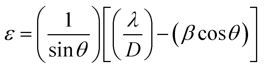
β and
θ are the full width at half maximum (FWHM) and Bragg's angle, respectively. Usually, internal stress will be formed in the film due to the change of temperature during annealing process, which deteriorates the quality of the film and the stability of the laminated device. In this paper, the stress of ZrO
2 films is evaluated by calculating the microstrain. The microstrain (
ε) of ZrO
2 films with different pre-annealing temperatures can be investigated by the following formula.
18| |
 | (3) |
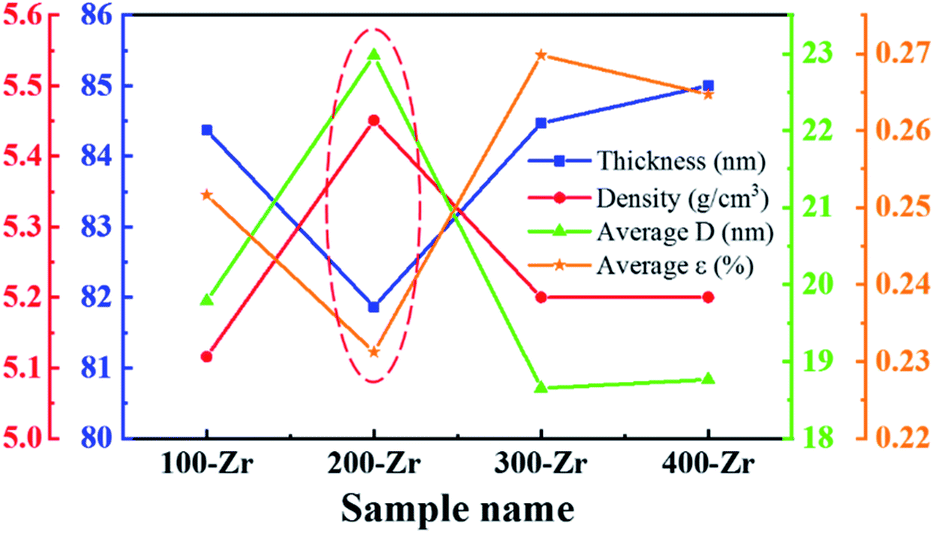
The structural parameters of ZrO2 films with different pre-annealing temperatures are listed in Table 1, and their trends are shown in Fig. 3. It was found that the ZrO2 film with pre-annealing temperature of 200 °C shown the optimal property, with the lowest average microstrain and the highest density. Typically, the purpose of the pre-annealing process is to remove the solvent and improve the quality of the subsequent film. When the pre-annealing temperature is too low, the solvent could not be completely removed. The residual solvent is covered by the subsequent film, leading to large roughness and low density. As a result, the ZrO2 film with pre-annealing temperature of 100 °C had the lowest density and the largest relative porosity. However, the solvent evaporates rapidly at a too high pre-annealing temperature, such as 300 and 400 °C, which also increases the porosity and reduces the density. In addition, the rapid evaporation of solvent also leads to greater residual stress, so the ZrO2 films with pre-annealing temperatures of 300 and 400 °C exhibited a large average microstrain. As the pre-annealing temperature increased from 100 °C to 400 °C, the intensity of the (111) crystal plane decreased first, reaching a minimum at 200 °C, and then it had a recovery. Since the XRD diffraction intensity was related to the content, ZrO2 film with pre-annealing temperature of 200 °C contained the lowest amount of monoclinic structure phase, showing a purer structure.
 |
| | Fig. 3 Structural parameters of ZrO2 films with different pre-annealing temperatures. | |
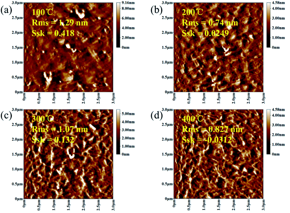
As shown in Fig. 4, in order to explore the relationship between pre-annealing temperature and surface topography, atomic force microscopy (AFM) measurement was carried out with a scanning area of 3.0 × 3.0 μm2. Root mean square (Sq) was used to describe the surface morphology of ZrO2 films, which was obtained by calculating the standard deviation of surface height. ZrO2 film with pre-annealing temperature of 200 °C shown the smoothest surface topography, with a root mean square of 0.74 nm. The ZrO2 film with pre-annealing temperature of 100 °C shown the largest roughness due to the inefficient evaporation of the solvent. When the pre-annealing temperature reached 300 and 400 °C, the ZrO2 films had a rough surface with holes and cracks. The surface skewness (Ssk), described the asymmetry of the height distribution histogram, and was defined by the following formula.
| |
 | (4) |
 |
| | Fig. 4 AFM diagrams of ZrO2 films with different pre-annealing temperatures. (a) 100 °C, (b) 200 °C, (c) 300 °C and (d) 400 °C. | |
A represents the scanning area, and Z (x, y) is the height of point (x, y). A positive Ssk value means a flat surface with peaks, while a negative one can be associated with a bearing surface with holes. When the Ssk = 0, a symmetric height distribution is indicated. It was found that ZrO2 film with pre-annealing temperature of 200 °C exhibited a symmetrical height distribution (peaks and valleys), with a Ssk of 0.0249.
2.2 The effect of post-annealing temperature
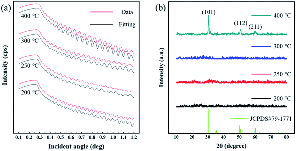
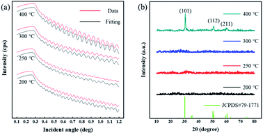
Based on the discussion above, the optimal pre-annealing temperature was 200 °C. Then, ZrO2 films were fabricated with a pre-annealing temperature of 200 °C, and the post-annealing temperature was set to 200, 250, 300 and 400 °C (for 1 hour). These films were labelled as Zr-200, Zr-250, Zr-300 and Zr-400, respectively. Fig. 5 is XRR and XRD spectra of ZrO2 films with different post-annealing temperatures. The crystallization of ZrO2 films annealed at different temperatures was measured by XRD, as shown in Fig. 5(b). Except for the ZrO2 film post-annealed at 400 °C, the ZrO2 films annealed at the other three temperatures were amorphous, which was consistent with the TG-DSC result. The diffraction peaks located at 30.3°, 50.7°, and 60.2° can be associated with (101), (112), and (211) crystal faces, respectively [tetragonal structure, JCPDS#79-1771].
 |
| | Fig. 5 (a) The XRR result of ZrO2 films with different post-annealing temperatures. (b) XRD spectra the ZrO2 films at different post-annealing temperatures. | |
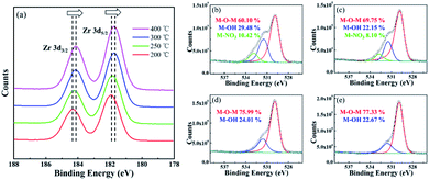
Fig. 6 shows the XPS results of the ZrO2 films with different post-annealing temperatures. As shown in Fig. 6(a), the Zr 3d5/2 peak located at 182.7 eV represented the metal–oxygen–metal (M–O–M) components while the Zr 3d3/2 peak located at 185.1 eV indicated the spin–orbit component. A shift to lower binding energies was observed when the post-annealing temperature increased, which can be associated with the oxidation behaviour from Zr(NO3)4 to ZrO2.19 In Fig. 6(b–e), the oxygen 1s peak can be divided into three peak components. The peaks located at 530.0 eV, 531.5 eV and 532.8 eV can be associated with M–O–M component, M–OH component and M–NO3 component, respectively.20 The M–O–M component indicates the formation of metal–oxygen–metal framework. The M–OH component was derived from the hydrolysis reaction between Zr4+ ion and 2-MOE, and the M–NO3 component can be attributed to the residual Zr(NO3)4 solute. Both of the M–OH component and M–NO3 component are associated with defect states in ZrO2 films. These impurity components will introduce defect levels into the forbidden band, thus declining the dielectric properties of the ZrO2 film. As the post-annealing temperature increased, both M–OH component and M–NO3 component decreased. When the post-annealing temperature up to 300 °C, M–NO3 component in the film was almost completely removed, which was consistent with N 1s spectra of ZrO2 films with different post-annealing temperatures (ESI Fig. 1†).
 |
| | Fig. 6 (a) Zr 3d spectra of the ZrO2 films with different post-annealing temperatures. (b–e) O 1s spectra of ZrO2 films with different post-annealing temperatures. (b) 200 °C, (c) 250 °C, (d) 300 °C and (e) 400 °C. | |
Table 2 is the structural parameters of ZrO2 films with different post-annealing temperatures, and the trend of these parameters is shown in Fig. 7. It was found that the thickness of ZrO2 film decreased rapidly as the post-annealing temperature increased from 200 to 300 °C. Since then it flattened off at a level of around 84 nm. Due to the evaporation of solvent and the decomposition of impurity, ZrO2 films prepared by solution-phase method may have many pores and defects.21 Therefore, high temperature heat treatment is required to promote atom rearrangement, thereby forming a denser film. As the post-annealing temperature increased, the density of ZrO2 films increased and the relative porosity volume decreased, which meant that a high post-annealing temperature is advantageous for obtaining a dense film. The percentage of M–O–M component increased with increasing post-annealing temperature, which was associated with the removal of impurities and orderly arrangement of atoms under high temperature.
Table 2 Structural parameters of ZrO2 films with different post-annealing temperatures
| Sample name |
Thickness (nm) |
Density (g cm−3) |
Relative porosity volume (%) |
O 1s spectra (%) |
| M–O–M |
M–OH |
M–NO3 |
| Zr-200 |
104.05 |
4.30 |
24.26 |
60.10 |
29.48 |
10.42 |
| Zr-250 |
92.63 |
4.66 |
17.98 |
69.75 |
22.15 |
8.10 |
| Zr-300 |
84.73 |
4.95 |
12.82 |
75.99 |
24.01 |
— |
| Zr-400 |
83.55 |
5.11 |
10.04 |
77.33 |
22.67 |
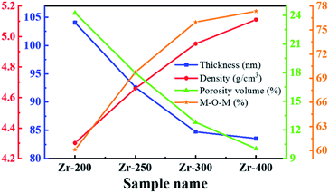 |
| | Fig. 7 Structural parameters of ZrO2 films with different post-annealing temperatures. | |
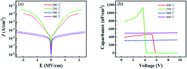
The dielectric performance of ZrO2 films with different post-annealing temperatures were measured by using an ITO/ZrO2/Al capacitor. As shown in Fig. 8, the films post-annealed at 200 °C and 250 °C showed the largest leakage current density due to high concentration of defect states. The ZrO2 films post-annealed at 300 °C and 400 °C exhibited excellent dielectric properties, with a leakage current density of 3.27 × 10⁻⁶ A cm−2 and 2.261 × 10⁻⁶ A cm−2 at 1 MV cm−1, respectively. For the capacitance–voltage curve, the capacitance density of ZrO2 films post-annealed at 200 °C and 250 °C gradually decrease to around zero due to the large leakage current. And the capacitance density of ZrO2 films post-annealed at 300 °C and 400 °C hardly changed with voltage, exhibiting excellent dielectric properties. The ZrO2 film post-annealed at 300 °C had a capacitance density of 320 nF cm−2 and a dielectric constant (k) of 19, while the 400 °C annealed ZrO2 film shown a capacitance density of 500 nF cm−2 and a higher dielectric constant (k) of 30.
 |
| | Fig. 8 The dielectric properties of ZrO2 films with different post-annealing temperatures. (a) Leakage current density–electric field curve, (b) capacitance–voltage curve. | |
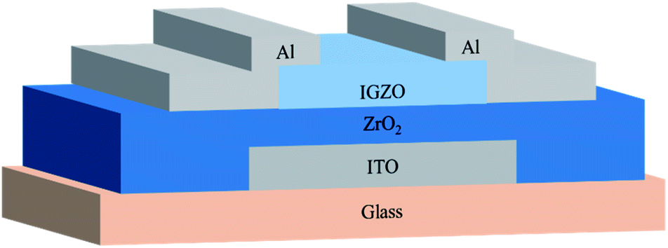
Based on the ZrO2 films with different post-annealing temperatures, bottom-gate top-contact IGZO/ZrO2 TFTs were fabricated, as shown in Fig. 9. The solution-processed ZrO2 films were deposited on the ITO/glass substrate. The IGZO films were produced by RF magnetron sputtering with a pressure of 5 mTorr (O2:Ar = 5%) and then annealed at 200 °C for 1 hour. The atomic ratio composition of the IGZO target is In:Ga:Zn:O = 1:1:1:4. Finally, aluminium electrodes with a thickness of 100 nm were fabricated above IGZO films by direct current (DC) sputtering a pressure of 1 mTorr (O2:Ar = 0%).
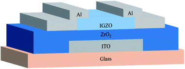 |
| | Fig. 9 Schematic diagram of IGZO-TFTs based on ZrO2 dielectric. | |
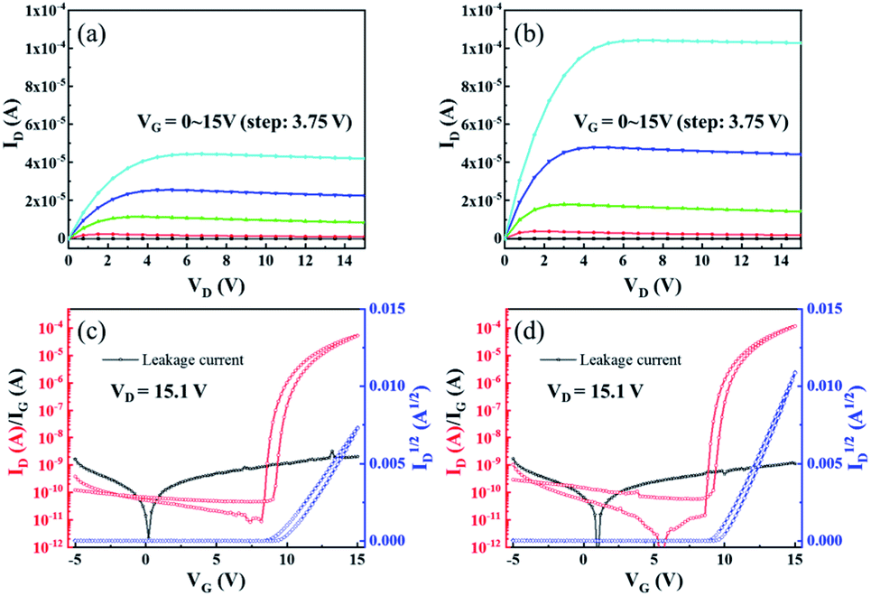
Most of previous reports only discussed the effect of thermal annealing on the electrical properties of dielectric layer, and the effect on the interface between dielectric layer and semiconductor was not evaluated. In this study, the interface between IGZO and ZrO2 films was investigated by micro-wave photoconductivity decay (μ-PCD). μ-PCD is a non-contact and non-destructive technology, which measures the microwave reflectivity of the photo-carrier trapping and recombination to evaluate defect state density of thin film or interface.22,23 Fig. 10(a–d) is the μ-PCD mapping result of IGZO-TFT with ZrO2 films under different post-annealing temperatures. The reflectivity peak signal (mean value), causing by the recombination of photo-generated carriers, shown an upward trend, which meant that the concentration of shallow localized defects on IGZO/ZrO2 stack decreased as the post-annealing temperature increased. Fig. 10(e) shows the μ-PCD decay curve of IGZO/ZrO2 stack and the decay curve consists of two parts, fast and slow decay curves.24 The fast decay curve is associated to the recombination processes,23 while the slow decay curve is related with the concentration of shallow localized defects.25 The μ-PCD slow decay time (τ2) of IGZO-TFTs with ZrO2 films post-annealed at 200, 250, 300 and 400 °C were 0.19, 0.16, 0.14 and 0.11 μs, respectively. A short τ2 also can be associated with a lower concentration of shallow localized defects,24 indicating that the interface between IGZO and ZrO2 films can be optimized by increasing the post-annealing temperature. Fig. 11 is the output and transfer curves of IGZO TFTs with ZrO2 gate dielectrics post-annealed at 300 and 400 °C. Since TFTs based on ZrO2 dielectrics post-annealed at 200 and 250 °C exhibited poor electrical characteristics, their curves were not shown. The electrical characteristics of ZrO2 films and corresponding TFT devices were listed in Table 3. The TFT with ZrO2 film post-annealed at 400 °C shown the highest mobility, which is consistent with the fact that IGZO/ZrO2 stack with the 400 °C post-annealed ZrO2 film had the largest μ-PCD peak mean value. Meanwhile, TFT with the 400 °C post-annealed ZrO2 dielectric exhibited a larger on state current, revealing a better interface between IGZO and ZrO2. Furthermore, the ΔVth of TFT with ZrO2 dielectric post-annealed at 400 °C is smaller, indicating that the concentration of the bulk and surface defects can be reduced by thermal annealing. As a conclusion, the post-annealing process can not only reduce internal defects of the dielectric, but also optimize the interface between semiconductor and dielectric, thus improving the electrical performance of TFTs.
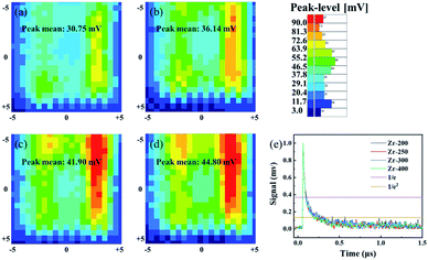 |
| | Fig. 10 The μ-PCD mapping result of IGZO-TFT with ZrO2 films under different post-annealing temperatures. (a) 200 °C, (b) 250 °C, (c) 300 °C and (d) 400 °C. (e) The μ-PCD decay curve of IGZO/ZrO2 stack with ZrO2 films under different post-annealing temperatures. | |
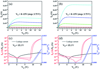 |
| | Fig. 11 (a) The output curve of IGZO TFT with ZrO2 gate dielectric post-annealed at 300 °C. (b) The output curve of IGZO TFT with ZrO2 gate dielectric post-annealed at 400 °C. (c) The transfer curve of IGZO TFT with ZrO2 gate dielectric post-annealed at 300 °C. (d) The transfer curve of IGZO TFT with ZrO2 gate dielectric post-annealed at 400 °C. | |
Table 3 The electrical characteristics of ZrO2 films and corresponding TFT devices
| Sample name |
Electrical characteristics of ZrO2 films with different post-annealing temperatures |
Electrical characteristics of TFT devices on ZrO2 films with different post-annealing temperatures |
| J (A cm−2) @ 1 MV cm−1 |
Dielectric constant |
μ-PCD peak mean (mV) |
μ-PCD slow decay time (μs) |
Mobility (cm2 (V s)−1) |
Ion/Ioff |
Vth (V) |
ΔVth (V) |
SS (V dec−1) |
| Zr-200 |
1.49 × 10⁻⁴ |
∼32 |
30.75 |
0.19 |
— |
— |
— |
— |
— |
| Zr-250 |
4.28 × 10⁻⁴ |
∼52 |
36.14 |
0.16 |
| Zr-300 |
3.27 × 10⁻⁶ |
∼19 |
41.90 |
0.14 |
13.14 |
1.18 × 10⁶ |
9.82 |
0.88 |
0.16 |
| Zr-400 |
2.26 × 10⁻⁶ |
∼30 |
44.80 |
0.11 |
16.34 |
2.08 × 10⁶ |
9.94 |
0.56 |
0.17 |
3. Experimental
The ZrO2 solution was synthesized by dissolving 0.5 M zirconium nitrate pentahydrate [Zr(NO3)4·5H2O] in 2-methoxyethanol, and then the solution was stirred vigorously for 24 hour and then were aged for 48 hour under ambient conditions. The thermal behaviour of the ZrO2 precursor was measured by thermogravimetric differential scanning calorimetry (TG-DSC) and the heating rate was 10 °C min−1. Fourier Transform infrared spectroscopy.
The crystallization of ZrO2 films was measured by X-ray diffraction (XRD) (EMPYREAN, PANalytical, Almelo, The Netherlands). X-ray reflectivity (XRR) (The instrument is the same as XRD) was used to investigate the thicknesses and densities of ZrO2 films. The chemical composition of ZrO2 films was obtained by X-ray photoelectron spectroscopy (XPS) (Thermo Fisher Scientific, Waltham, MA, USA), and all peaks were calibrated by using the carbon 1s peak (284.8 eV) as a reference. Atomic force microscopy (AFM) (BY3000, Being Nano-Instruments, Beijing, China) was used to investigate the surface morphology of ZrO2 films. Metal insulator metal (MIM) capacitors were fabricated by sputtering circular aluminium electrodes with a thickness of 100 nm on the ZrO2 films, and Keithley4200 (Tektronix, Beaverton, Oregon, OR, USA) parameter analyser was used to investigate the electrical characteristics of MIM capacitors in air. IGZO film was fabricated by RF magnetron sputtering above ZrO2 film. The decay curve and mapping result of IGZO/ZrO2 stack was measured by μ-wave photo conductivity decay (μ-PCD) measurement system (KOBELCO, LTA-1620SP, Kobe, Japan).
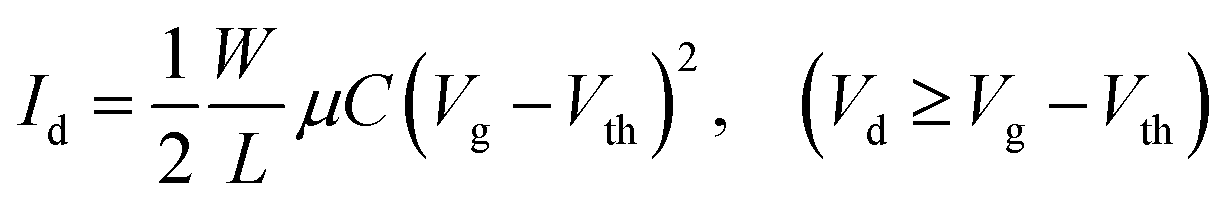
The semiconductor parameter analyser (Agilent4155C, Agilent, Santa Clara, CA, USA) was used to investigate the output and transfer curves of TFTs in air. The field-effect mobility (μ) and threshold voltage (Vth) can be measured according to the following eqn (1). The subthreshold swing (SS) was extracted by fitting the eqn (2):
| |
 | (5) |
| |
 | (6) |
μ and
C represent the field-effect mobility and dielectric layer capacitance.
Id,
Vth,
Vd and
Vg are drain current, threshold voltage, drain voltage and gate voltage, respectively. The length (
L) and width (
W) of channel are 325 and 515 μm, respectively.
4. Conclusions
In this paper, the thermal effect of pre-annealing and post-annealing process on solution-processed ZrO2 dielectric was discussed. The thermal effect of pre-annealing temperature was investigated by various analysis, such as XRD, XRR and AFM. It was found that the pre-annealing process had a significant effect on the density and internal stress of ZrO2 film. The ZrO2 film with pre-annealing temperature of 100 °C shown the largest relative porosity owing to the inefficient evaporation of the solvent. And ZrO2 films with pre-annealing temperature of 300 °C and 400 °C suffer from great residual stress and large pores due to the rapid evaporation of solvent. As for the post-annealing temperature, the post-annealing process can not only improve the electrical properties of ZrO2 dielectric, but also optimize the interface between semiconductor and dielectric. As a result, the TFT with a pre-annealing temperature of 200 °C and a post-annealing temperature of 400 °C showed the best electrical performance, with a mobility of 16.34 cm2 (V s)−1 and an Ion/Ioff of 2.08 × 10⁶.
Conflicts of interest
There are no conflicts to declare.
Acknowledgements
This work was supported by National Natural Science Foundation of China (Grant 51771074), National Science Foundation for Distinguished Young Scholars of China (Grant 51725505), Guangdong Natural Science Foundation (No. 2016A030313459 and 2017A030310028), Guangdong Science and Technology Project (No. 2016B090907001 and 2019B010934001) and the Fundamental Research Funds for the Central Universities.
Notes and references
- J. S. Park, W.-J. Maeng, H.-S. Kim and J.-S. Park, Thin Solid Films, 2012, 520, 1679–1693 CrossRef CAS.
- E. Fortunato, P. Barquinha and R. Martins, Adv. Mater., 2012, 24, 2945–2986 CrossRef CAS PubMed.
- W. Xu, M. Dai, L. Liang, Z. Liu, X. Sun, Q. Wan and H. Cao, J. Phys. D: Appl. Phys., 2012, 45, 205103–205107 CrossRef.
- K. Nomura, H. Ohta, A. Takagi, T. Kamiya, M. Hirano and H. Hosono, Nature, 2004, 432, 488–492 CrossRef CAS PubMed.
- J. Cho, P. Choi, N. Lee, S. Kim and B. Choi, J. Nanosci. Nanotechnol., 2016, 16, 10380–10384 CrossRef CAS.
- R. S. Chen, W. Zhou, M. Zhang and H. S. Kwok, Thin Solid Films, 2012, 520, 6681–6683 CrossRef CAS.
- W. K. Lin, K. C. Liu, S. T. Chang and C. S. Li, Thin Solid Films, 2012, 520, 3079–3083 CrossRef CAS.
- S. M. Bobade, J. H. Shin, Y. J. Cho, J. S. You and D. K. Choi, Appl. Surf. Sci., 2009, 255, 7831–7833 CrossRef CAS.
- L. Liao, J. Bai, Y.-C. Lin, Y. Qu, Y. Huang and X. Duan, Adv. Mater., 2010, 22, 1941–1945 CrossRef CAS PubMed.
- W. Zhang, Y. Cui, Z. G. Hu, W. L. Yu, J. Sun, N. Xu, Z. F. Ying and J. D. Wu, Thin Solid Films, 2012, 520, 6361–6367 CrossRef CAS.
- Y. Son, A. Liao and R. L. Peterson, J. Mater. Chem. C, 2017, 5, 8071–8081 RSC.
- C.-M. Kang, H. Kim, Y.-W. Oh, K.-H. Baek and L.-M. Do, J. Nanosci. Nanotechnol., 2017, 17, 3293–3297 CrossRef CAS.
- C.-Y. Tsay and T.-Y. Yan, J. Phys. Chem. Solids, 2014, 75, 142–147 CrossRef CAS.
- Y.-H. Chen, C.-J. Su, C. Hu and T.-L. Wu, IEEE Electron Device Lett., 2019, 40, 467–470 CAS.
- S. Park, C.-H. Kim, W.-J. Lee, S. Sung and M.-H. Yoon, Mater. Sci. Eng., R, 2017, 114, 1–22 CrossRef.
- S. Zhou, Z. Fang, H. Ning, W. Cai, Z. Zhu, J. Wei, X. Lu, W. Yuan, R. Yao and J. Peng, Appl. Sci., 2018, 8, 806 CrossRef.
- G. Turgut, E. F. Keskenler, S. Aydin, M. Yilmaz, S. Dogan and B. Duzgun, Phys. Scr., 2013, 87, 035602 CrossRef.
- R. R. Kasar, N. G. Deshpande, Y. G. Gudage, J. C. Vyas and R. Sharma, Phys. B, 2008, 403, 3724–3729 CrossRef CAS.
- J. H. Park, Y. B. Yoo, K. H. Lee, W. S. Jang, J. Y. Oh, S. S. Chae and H. K. Baik, ACS Appl. Mater. Interfaces, 2013, 5, 410–417 CrossRef CAS PubMed.
- W. Cai, Z. Zhu, J. Wei, Z. Fang, H. Ning, Z. Zheng, S. Zhou, R. Yao, J. Peng and X. Lu, Materials, 2017, 10, 972 CrossRef PubMed.
- D. J. Kim, D. L. Kim, Y. S. Rim, C. H. Kim, W. H. Jeong, H. S. Lim and H. J. Kim, ACS Appl. Mater. Interfaces, 2012, 4, 4001–4005 CrossRef CAS PubMed.
- X. Liu, W. Cai, J. Chen, Z. Fang, H. Ning, S. Hu, R. Tao, Y. Zeng, Z. Zheng, R. Yao, M. Xu, L. Wang, L. Lan and J. Peng, J. Phys. D: Appl. Phys., 2016, 49, 505102 CrossRef.
- R. Yao, Z. Zheng, M. Xiong, X. Zhang, X. Li, H. Ning, Z. Fang, W. Xie, X. Lu and J. Peng, Appl. Phys. Lett., 2018, 112, 103503 CrossRef.
- S. Yasuno, T. Kugimiya, S. Morita, A. Miki, F. Ojima and S. Sumie, Appl. Phys. Lett., 2011, 98, 102107 CrossRef.
- C. Zhu, A. Liu, G. Liu, G. Jiang, Y. Meng, E. Fortunato, R. Martins and F. Shan, J. Mater. Chem. C, 2016, 4, 10715–10721 RSC.
Footnote |
| † Electronic supplementary information (ESI) available. See DOI: 10.1039/c9ra06132k |
|
| This journal is © The Royal Society of Chemistry 2019 |
Click here to see how this site uses Cookies. View our privacy policy here. 
 Open Access Article
 This Open Access Article is licensed under a Creative Commons Attribution-Non Commercial 3.0 Unported Licence
 a,
Jianhua Zhangb,
Zhiqiang Fang
a,
Jianhua Zhangb,
Zhiqiang Fang