 Open Access Article
One-step solution synthesis of a two-dimensional semiconducting covalent organometallic nanosheet via the condensation of boronic acid†
Qijun Wang‡
a,
Jiahao Yan‡b,
Mingchao Xiao‡ac,
Devaraj Manoj‡a,
Cheng Zhonge,
Qiying Lv a,
Lite Yanga,
Liangmei Wub,
Zhuoping Wanga,
Lihong Bao
 *b,
Hongjun Gao
 b,
Fei Xiaoa,
Lang Jiang
 c and
Shuai Wang
 *ad
*ad
aSchool of Chemistry and Chemical Engineering, Huazhong University of Science & Technology, Wuhan, 430074, P. R. China. E-mail: chmsamuel@mail.hust.edu.cn
bInstitute of Physics, Chinese Academy of Sciences, Beijing 100190, P. R. China. E-mail: lhbao@iphy.ac.cn
cInstitute of Chemistry, Chinese Academy of Sciences, Beijing 100190, P. R. China
dDepartment of Materials Science, Fudan University, Shanghai, 200433, P. R. China
eCollege of Chemistry and Molecular Sciences, Wuhan University, Wuhan, 430072, P. R. China
First published on 17th September 2019
Abstract
In this work, a 2D covalent organometallic nanosheet (COMS) was designed and successfully synthesized through the one-step conjunction of a terpyridine–metal–terpyridine (TMT) sandwich coordinate motif with borate ester covalent heterocyclic (B3O3) linkage via the condensation of boronic acid. The obtained 2D COMS with a cobalt coordination center (2D COMS-Co) showed promising p-type semiconducting properties.
Two-dimensional (2D) metal–organic frameworks (MOFs) obtained by using the strong bonding effects between metal ions and organic molecule species have aroused great interest;1–8 these include coordination nanosheets, which are a class of 2D materials featuring metal complex motifs.9–12 Covalent bonds are considered to be an effective way to fabricate covalent organic frameworks (COFs) such as COF-1, which is mainly constructed by a phenyl ring and borate ester to form covalent heterocyclic (B3O3) linkage.13–15 Based on the synergistic effects of metal coordination and covalent interactions, Jiang and co-workers demonstrated the important role of central metals in controlling π-electronic functions through Mpc-COF.16 Nevertheless, the coordination bond forms spontaneously within the ring of the porphyrin heterocycle and not as the linkage between organic components. In addition, the connections made between metal ions and ligand motifs cannot facilitate the proper tuning of the physicochemical properties of the structure.17 Combining the covalent and coordinate features may provide an opportunity to design new 2D materials and thus, the synergetic enhancement in many unique properties can be achieved. As far as we know, the fabrication of 2D semiconducting materials that combine the covalent heterocyclic linkage and coordinate linkage has not been reported. Therefore, it is a pressing need to construct a functional 2D organic framework through a one-step synthesis strategy, which would be a more attractive approach.
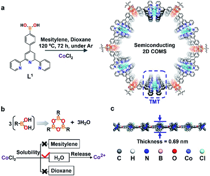
Herein, we first proposed an efficient one-step strategy to synthesize a 2D material by the synergy of covalent and organometallic interactions; it was named as a covalent organometallic nanosheet (2D COMS-M, M = cobalt (Co)). The as-proposed 2D COMS-Co was constructed by linking the borate ester covalent heterocyclic (B3O3) structure and terpyridine (tpy) metal coordination motif (TMT) (Fig. 1).
 | ||
| Fig. 1 (a) Synthesis route of the semiconducting 2D COMS. (b) Design principles of COMS via the condensation of boronic acid. (c) The calculated cross-sectional view of 2D COMS-Co. | ||
In order to explore the extended construction of 2D COMS, the self-condensation ligand 4-phenylborate-2,2′; 6′,2′′-terpyridine (L1) integrated with CoCl2 as the Co2+ carrier was employed through an anhydrous and oxygen-free hydrothermal reaction at 120 °C under argon, and the typical synthesis process is depicted in Fig. 1a (for details, please see ESI†). Starting from the condensation reaction of boronic acid (Fig. 1b), H2O could be generated and played a key role in dissolving CoCl2 and further releasing Co2+ ions (CoCl2 is practically insoluble in mesitylene and dioxane). This was followed by coordination between the terpyridine motifs and the released Co2+ ions to obtain 2D COMS. This novel strategy could achieve crystalline 2D materials by self-controlling the release of Co2+ through the one-step condensation reaction of boronic acid. The calculated cross-sectional view of 2D COMS-Co indicates that the thickness of the monolayer 2D COMS-Co is 0.69 nm (Fig. 1c). The dual synergistic connecting effects of covalence and coordination in 2D COMS-Co provided nanosheet-like morphology with significant improvement in the semiconducting performance. The hole mobility of the 2D COMS-Co-based FET device could reach to 5.7 × 10⁻⁵ cm2 V−1 s−1 with an ON–OFF ratio of 221, which demonstrated the potential application of 2D COMS-Co in semiconducting devices.
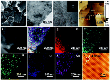
The scanning electron microscopy (SEM) image (Fig. 2a) reveals that 2D COMS-Co has a uniform micron-sized nanosheet-like structure. Furthermore, the transmission electron microscopy (TEM) image indicates that the as-synthesized 2D COMS-Co consists of few multi-layers. Fig. 2c shows an enlarged image of the selected area visualized with high-resolution TEM (HRTEM), where the section enclosed by white lines depicts lattice fringes. Moreover, the selected area electron diffraction (SAED, inset of Fig. 2c) image shows a circular ring pattern that reveals the well-defined crystalline structure of 2D COMS-Co; these results are in agreement with our X-ray diffraction data (Fig. S2, ESI†). Most interestingly, the atomic force microscopy (AFM) image (Fig. 2d) clearly demonstrates that the selected thickness of 2D COMS-Co is 2.07 nm, and the resultant thickness is three times less than the calculated value of 0.69 nm (Fig. 1c), indicating its uniform three-layer stacked structure. The above results collectively provide strong evidence of typical 2D features for COMS-Co. Moreover, the high-angle annular dark-field (HAADF) image and the scanning transmission electron microscopy (STEM) elemental mapping further revealed that the C (red), B (cyan), N (green), O (blue) and Co (pink) elements are homogeneously distributed on the selected area of 2D COMS-Co (Fig. 2e–k). The electronic structure of 2D COMS-Co was further characterized by four-probe scanning tunnel microscopy (STM) (please see details in ESI†). The high-resolution STM imaging revealed that the 2D COMS-Co flake has a layered flake structure with uniformly distributed hexagonal hole morphology and the resultant holes have a diameter of 4.72 nm (Fig. 2l); this observation is in accordance with the proposed structure of 2D COMS-Co (Fig. S8, ESI†).
 | ||
| Fig. 2 Morphological characterization of 2D COMS-Co. (a) SEM image of powder. (b) TEM image. (c) HRTEM image (d) AFM image. (e) HAADF image. (f–k) STEM elemental mapping. (l) STM image. | ||
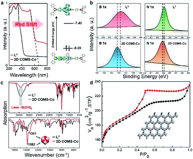
Due to the covalence and coordination effects, the absorption peak of 2D COMS-Co obtained from the UV-vis measurements (Fig. 3a) is red-shifted in comparison to that for ligand L1, and the optical band gap is calculated to be 1.85 eV. Furthermore, density functional theory (DFT) calculations revealed that the highest occupied molecular orbital (HOMO) of 2D COMS-Co was dominated by the π orbital of the B3O3 linkage and the phenyl ring, whereas the π* orbital of TMT was responsible for the lowest unoccupied molecular orbital (LUMO). Additionally, the calculated electronic band gap of 2D COMS-Co was 1.89 eV, which was in accordance with the optical band gap, confirming the successful synthesis of 2D COMS-Co. Fig. 3b displays the X-ray photoelectron spectroscopy (XPS) spectrum of 2D COMS-Co, in which the appearance of the binding energy peak at 192.2 eV is significantly different from that for L1 (191.1 eV), which can be ascribed to the –C–B–O2 structure.18,19 Compared to the observation for L1, the N 1s peak for 2D COMS-Co shifted to a higher binding energy value (399.2 eV for COMS-Co and 397.5 eV for L1). The skewing of the peaks toward higher binding energy was induced by the contribution of N atoms in terpyridine to the metal center. Therefore, the XPS results clearly provide evidence of the existence of both covalent and coordination effects in the as-prepared 2D COMS-Co. The Fourier transform infrared (FT-IR) spectra in Fig. 3c show that the –B(OH)2 bands (around 3500 cm−1) of the ligand L1 are significantly attenuated compared to that observed for 2D COMS-Co. In addition, the B–O stretching vibrations at 1351 cm−1 can be observed for 2D COMS-Co but not for L1.13,20–22 Thus, the above results show that the expected B3O3 rings for 2D COMS-Co have indeed been formed. Notably, the nitrogen adsorption–desorption isotherms reveal that the Brunauer–Emmett–Teller (BET) specific surface area of 2D COMS-Co is as high as 598 m2 g−1 (Fig. 3d); it surpasses those of other layered materials, including the reported graphene oxide paper (10 m2 g−1), clays (10 to 100 m2 g−1), and pillared clays (50 to 300 m2 g−1), and is in the range of the values of the most porous zeolites and many porous carbons.13,23 This drastic enhancement can be assigned to the uniform porous structure of the as-synthesized 2D COMS-Co.
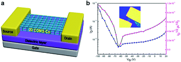
The above results show that the 2D COMS-Co units arranged in periodic strips can provide conducting pathways for charge carrier transport through TMT and central cobalt ions. 2D COMS-Co was employed to function as the active semiconducting channel in a field-effect transistor (FET) device. As shown in Fig. 4a, the individual 2D COMS-Co sample is deposited on an Si wafer as the semiconducting layer to construct the FET device. The 2D COMS-Co-based FET device delivered hole mobility of 5.7 × 10⁻⁵ cm2 V−1 S−1 and an ON/OFF ratio of 221, which were comparable with those of previously reported 2D MOFs (Table S1†). Therefore, these results collectively demonstrate the potential application of 2D COMS-Co in semiconducting devices.
In summary, a novel two-dimensional covalent organometallic nanosheet (COMS) was designed and successfully synthesized through the strategy of one-step conjunction of a TMT sandwich coordinate motif with B3O3 linkage. This facile strategy could achieve crystalline 2D COMS-Co by self-controlling the release of Co2+ through a one-step condensation reaction of boronic acid. The systematic characterization demonstrated the successful preparation of porous and crystalline 2D COMS-Co. Particularly, the as-prepared 2D COMS-Co-based FET device presented hole mobility of 5.7 × 10⁻⁵ cm2 V−1 S−1 and an ON/OFF ratio of 221, which demonstrated the potential application of 2D COMS-Co in semiconducting devices. Therefore, we envision that this work will open a new avenue for the synthesis of two-dimensional semiconducting covalent organometallic materials by using covalence and coordination dual synergistic connection effects via a one-step facile strategy.
Conflicts of interest
There are no conflicts to declare.Acknowledgements
The research was supported by the National Natural Science Foundation of China (Project No. 51772110, No. 51572094 and No. 51873160). All authors are grateful for characterization and computing service from the Analytical and Testing Center of HUST and the Wuhan National Laboratory for Optoelectronics, respectively.Notes and references
- A. J. Clough, J. W. Yoo, M. H. Mecklenburg and S. C. Marinescu, J. Am. Chem. Soc., 2015, 137, 118–121 CrossRef CAS PubMed.
- R. Dong, M. Pfeffermann, H. Liang, Z. Zheng, X. Zhu, J. Zhang and X. L. Feng, Angew. Chem., Int. Ed., 2015, 54, 12058–12063 CrossRef CAS PubMed.
- E. M. Miner, T. Fukushima, D. Sheberla, L. Sun, Y. Surendranath and M. Dinca, Nat. Commun., 2016, 7, 10942–10948 CrossRef CAS PubMed.
- R. Sakamoto, T. Yagi, K. Hoshiko, S. Kusaka, R. Matsuoka, H. Maeda, Z. Liu, Q. Liu, W. Y. Wong and H. Nishihara, Angew. Chem., Int. Ed., 2017, 56, 3526–3530 CrossRef CAS PubMed.
- T. Kambe, R. Sakamoto, T. Kusamoto, T. Pal, N. Fu-kui, T. Shimojima, Z. Wang, T. Hirahara, K. Ishizaka, S. Hasegawa, F. Liu and H. Nishihara, J. Am. Chem. Soc., 2014, 136, 14357–14360 CrossRef CAS PubMed.
- R. Makiura, S. Motoyama, Y. Umemura, H. Yama-naka, O. Sakata and K. Hiroshi, Nat. Mater., 2010, 9, 565–571 CrossRef CAS PubMed.
- R. H. Dong, P. Han, H. Arora, M. Ballabio, M. Kara-kus, Z. Zhang, C. Shekhar, P. Alder, P. S. Petkov, A. Erbe, S. C. B. Mannsfeld, C. Felser, T. Heine, M. Bonn, X. L. Feng and E. Cánovas, Nat. Mater., 2018, 17, 1027–1032 CrossRef CAS PubMed.
- H. Sahabudeen, H. Y. Qi, B. A. Glatz, D. Tranca, R. H. Dong, Y. Hou, T. Zhang, C. Kuttner, T. Lehnert, G. Seifert, U. Kaiser, A. Fery, Z. K. Zheng and X. L. Feng, Nat. Commun., 2016, 7, 13461–13468 CrossRef PubMed.
- T. Kambe, R. Sakamoto, K. Hoshiko, K. Takada, M. Miyachi, J. H. Ryu, S. Sasaki, J. Kim, K. Nakazato, M. Takata and H. Nishihara, J. Am. Chem. Soc., 2013, 135, 2462–2465 CrossRef CAS PubMed.
- Z. K. Zheng, L. Opilik, F. Schiffmann, W. Liu, G. Ber-gamini, P. Ceroni, L. T. Lee, A. Schütz, J. Sakamoto, R. Zenobi, J. VandeVondele and A. D. Schlüter, J. Am. Chem. Soc., 2014, 136, 6103–6110 CrossRef CAS PubMed.
- R. Sakamoto, K. Hoshiko, Q. Liu, T. Yaji, T. Naga-yama, S. Kusaka, M. Tsuchiya, Y. Kitagawa, W. Y. Wong and H. Nishihara, Nat. Commun., 2015, 6, 6713–6721 CrossRef CAS PubMed.
- K. Takada, R. Sakamoto, S. T. Yi, S. Katagiri, T. Kambe and H. Nishihara, J. Am. Chem. Soc., 2015, 137, 4681–4689 CrossRef CAS PubMed.
- A. P. Côtê, A. I. Benin, N. W. Ockwig, M. O'Keeffe, A. J. Matzger and O. M. Yaghi, Science, 2005, 310, 1166–1170 CrossRef PubMed.
- C. J. Doonan, D. J. Tranchemontagne, T. G. Glover, J. R. Hunt and O. M. Yaghi, Nat. Chem., 2010, 2, 235–238 CrossRef CAS PubMed.
- X. Feng, L. L. Liu, Y. Honsho, A. Saeki, S. Seki, S. Irle, Y. P. Dong, A. Nagai and D. L. Jiang, Angew. Chem., Int. Ed., 2012, 51, 2618–2622 CrossRef CAS PubMed.
- X. S. Ding, X. Feng, A. Saeki, S. Seki, A. Nagai and D. L. Jiang, Chem. Commun., 2012, 48, 8952–8954 RSC.
- T. Tsukamoto, K. Takada, R. Sakamoto, R. Mat-suoka, R. Toyoda, H. Maeda, T. Yagi, M. Nishikawa, N. Shinjo, S. Amano, T. Iokawa, N. Ishibashi, T. Oi, K. Kanayama, R. Kinugawa, Y. Koda, T. Komu-ra, S. H. Nakajima, R. Fukuyama, N. Fuse, M. Mizui, M. Miyasaki, Y. Yamashita, K. Yamada, W. X. Zhang, R. C. Han, W. Y. Liu, T. Tsubomura and H. Nishi-hara, J. Am. Chem. Soc., 2017, 139, 5359–5366 CrossRef CAS PubMed.
- C. P. Yang, Y. X. Yin, T. G. Guo and L. J. Wan, J. Am. Chem. Soc., 2015, 137, 2215–2218 CrossRef CAS PubMed.
- Z. A. Ghazi, L. Y. Zhu, H. Wang, A. Naeem, A. M. Khattak, B. Liang, N. A. Khan, X. Wei, L. S. Li and Z. Y. Tang, Adv. Energy Mater., 2016, 6, 1601250–1601255 CrossRef.
- J. R. Hunt, C. J. Doonan, J. D. LeVangie, A. P. Côtê and O. M. Yaghi, J. Am. Chem. Soc., 2008, 130, 11872–11873 CrossRef CAS PubMed.
- H. M. EI-Kaderi, J. R. Hunt, J. L. Mendoza-Cortes, A. P. Côtê, R. E. Taylor, M. O'Keeffe and O. M. Yaghi, Science, 2007, 316, 268–272 CrossRef PubMed.
- F. J. Uribe-Romo, J. R. Hunt, H. Furukawa, C. Klöck, M. O'Keeffe and O. M. Yaghi, J. Am. Chem. Soc., 2009, 131, 4570–4571 CrossRef CAS PubMed.
- J. J. Liu, W. Zan, K. Li, Y. Yang, F. X. Bu and Y. X. Xu, J. Am. Chem. Soc., 2017, 139, 11666–11669 CrossRef CAS PubMed.
Footnotes |
| † Electronic supplementary information (ESI) available: Experimental details and additional data. See DOI: 10.1039/c9ra05806k |
| ‡ These authors are contributed equally to this work. |
| This journal is © The Royal Society of Chemistry 2019 |


