
 Open Access Article
 This Open Access Article is licensed under a Creative Commons Attribution-Non Commercial 3.0 Unported Licence
Effect of annealing temperature on silicon-based MoSx thin film solar cells
Haoyu Xu a,
Dongqiang Chena,
Litao Xina,
Heju Xu*b and
Wei Yu*a
a,
Dongqiang Chena,
Litao Xina,
Heju Xu*b and
Wei Yu*a
aCollege of Physics Science & Technology, Hebei University, Baoding, 071002, P. R. China. E-mail: xuhaoyu93@qq.com; 20171365@stumail.hbu.edu.cn
bCollege of Science, North China University of Science and Technology, Tangshan 063009, China. E-mail: 715179578@qq.com
First published on 21st October 2019
Abstract
A suitable annealing temperature was found by adopting the sol–gel method to prepare silicon-based molybdenum sulfide film heterojunction solar cells. As shown by the results, a change in the efficiency of the solar cells, which was attributed to the fact that as the annealing temperature rises, the degree of crystallization of the film increases continuously, the degree of order of the crystal particles goes up first and then goes down, and the temperature change affects the proportion of Mo in different valence states. By comparison, it was found that when the temperature reached 500 °C, the degree of order of the film was raised and the film was in the initial zone from the amorphous to the microcrystal phase change and the proportion of Mo 6+ was relatively large, increasing the conversion efficiency of the device power to 7.55% and laying a good basis for preparing high-performance solar batteries made in the two-dimensional materials. When the annealing temperature continues to rise, the intergranular defects increase, and the overall degree of order of the film decreases. Furthermore, the highly crystalline thin films and the improvement in the device efficiency can be controlled if we obtained the relationship between the annealing temperature and the layers of the two-dimensional materials.
1. Introduction
As typical materials of the transition metal disulfide compounds, two-dimensional MoS2 is characterized by strong optical absorption (∼5 × 105 cm−1), high carrier transfer (∼100 cm2 V−1 S−1) and high switch ratio (∼108)1 and the bandgap width changes from the single 1.9 eV to bulk materials 1.3 eV, but it can not only serve as the intercalated subject of the electrode materials of the high-energy density battery, but it can also serve as the ideal electrode materials.2,3 People have adopted many methods, such as the exfoliation method and chemical vapor deposition (CVD) method to prepare high-quality molybdenum sulfide films. O'Neill et al. adopted the ultrasonic solution exfoliation to better control the exfoliation of MoS2 flakes from the ordinary solution and the concentrated solution;4 Ji et al. took advantage of the van der Waals epitaxial technology and adopted the low-pressure CVD to synthesize the single-layer molybdenum sulfide film.5 However, even though the most original crystal quality can be obtained through the mechanical exfoliation, the yield rate is extremely low.6,7 The ion insertion technology has an effect on the changes of the crystal structure, but the solvent-based technology makes the sheet size small for manufacturing the electronic devices.7,8 The current growth technology can generate the sheet with larger crystals, but is usually at the expense of the crystal quality and control of the number of layers, and it is impossible to give consideration to both things. For the complete study and use of the new characteristics of MoS2, a more advanced synthetic technology is required to generate highly crystalline wafer-level MoS2 and better control its number of layers.The sol–gel method to prepare the films is a self-assembly method with low cost and high deposition rate to effectively control the stoichiometry, crystallinity, density and microstructure of the film.9 It is used to prepare a new type of thin polymer film with optical-electrical characteristic, and overcomes the defects of thin film processing, such as it is non-renewable, and poor adhesion between polymer film and substrate. Moreover, it is mainly characterized by a large film forming area with controllable and renewable film thickness and height. Mohammadi et al. adopted the sol–gel spinning coating technology to synthesize an indium tin molybdenum oxide (ITMO) film and improve the transfer rate of the carrier.10 Through the one-step spin-coating technique, Zheng et al. prepared the active layer and cathode sandwich of the high-performance inverted perovskite solar battery.11 Takenaka et al., through the sol–gel method, prepared and improved a single-layer lead zirconate titanate film, making it more transparent and free from cracks.12 Inspired by their experiments, it is believed that the sol–gel method can be used to prepare a low-cost and high-quality single-layer molybdenum sulfide film under the normal temperature.
During the study, we directly obtained the amorphous-microcrystal MoSx films on a p-Si substrate via the sol–gel method and prepared the precursor solution by the ultrasonic method under low temperature, using ethylene glycol (EG) as the solution. Through the sol–gel method, the p-Si substrate was coated with the precursor solution containing (NH4)2MoS4. Then, under the condition of a mixture of Ar and H2 gases at a flow rate of 150 sccm and 70 sccm, respectively, the amorphous-microcrystal MoSx films were prepared, and the effect of the annealing temperature on the microstructure and bonding characteristics of the amorphous-microcrystal MoSx film were analyzed by changing the annealing temperature. This procedure shows the adjustment mechanism of the microstructure of the MoSx film and amorphous-microcrystal phase change rules. The molybdenum sulfide film under different annealing temperatures was used for the ITO/MoSx/p-Si/p+-Si/Ag heterojunction solar cells. Through the analysis of the relation between the film structure and photoelectric conversion characteristic, the physical mechanism that limits the efficiency improvement of the heterojunction solar cells was studied.
2. Experimental section
2.1. Materials and syntheses
 | (1) |
2.2. Characterization
X-ray photoelectron spectrometer (ThermoFisher ESCALAB250X) was used to analyze the composition and valence states of the films under room temperature. The laser Raman spectrometer (HORIBA Jobin Yvon LabRAM HR Evolution) was used for measurement, and the wavelength and raster of the laser were 532 nm and 1800 gr·nm−1, respectively. The scanning image of MoSx was obtained using an atomic force microscope (Bruker). The spectral response curve of the solar cells was tested using the IPCE testing system (CROWNTECH) of the solar cells. The current density–voltage (J–V) was measured using the semiconductor device parameter analyzer (Agilent B1500A).3. Results and discussion
Fig. 1 is the Raman spectra of the samples prepared under different annealing temperatures. From the figure, it could be seen that all the samples showed the Raman peak corresponding to the A1g vibration mode. When the temperature was 500 °C, the Raman peak corresponding to the E12g vibration mode became relatively obvious, indicating that the degree of order of the film under this condition was higher.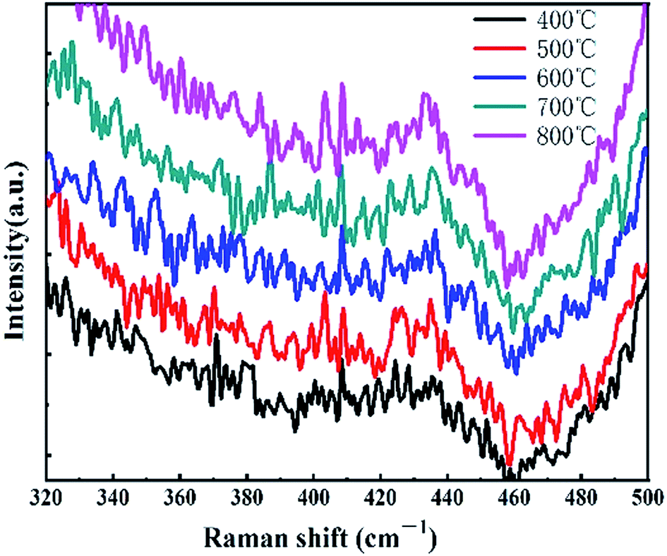 | ||
| Fig. 1 Raman spectrum of MoSx films at various annealing temperatures. | ||
Fig. 2(a)–(e) are the AFM topography of the MoSx film prepared under the annealing temperatures of 400 °C, 500 °C, 600 °C, 700 °C and 800 °C. From the figures, the MoSx film's surface prepared under 500 °C was relatively smooth. The flatness of the films was generally reduced first and then increased. Theoretically, with the increase in the annealing temperature, the MoSx film should gradually transfer from the amorphous state to the microcrystalline state with small crystal particles, where 500 °C is the transition area from the amorphous state to the microcrystalline state. Thereafter, the degree of order of the film destroyed as the temperature increased due to the formation of large crystal particles, which leads to increased roughness.
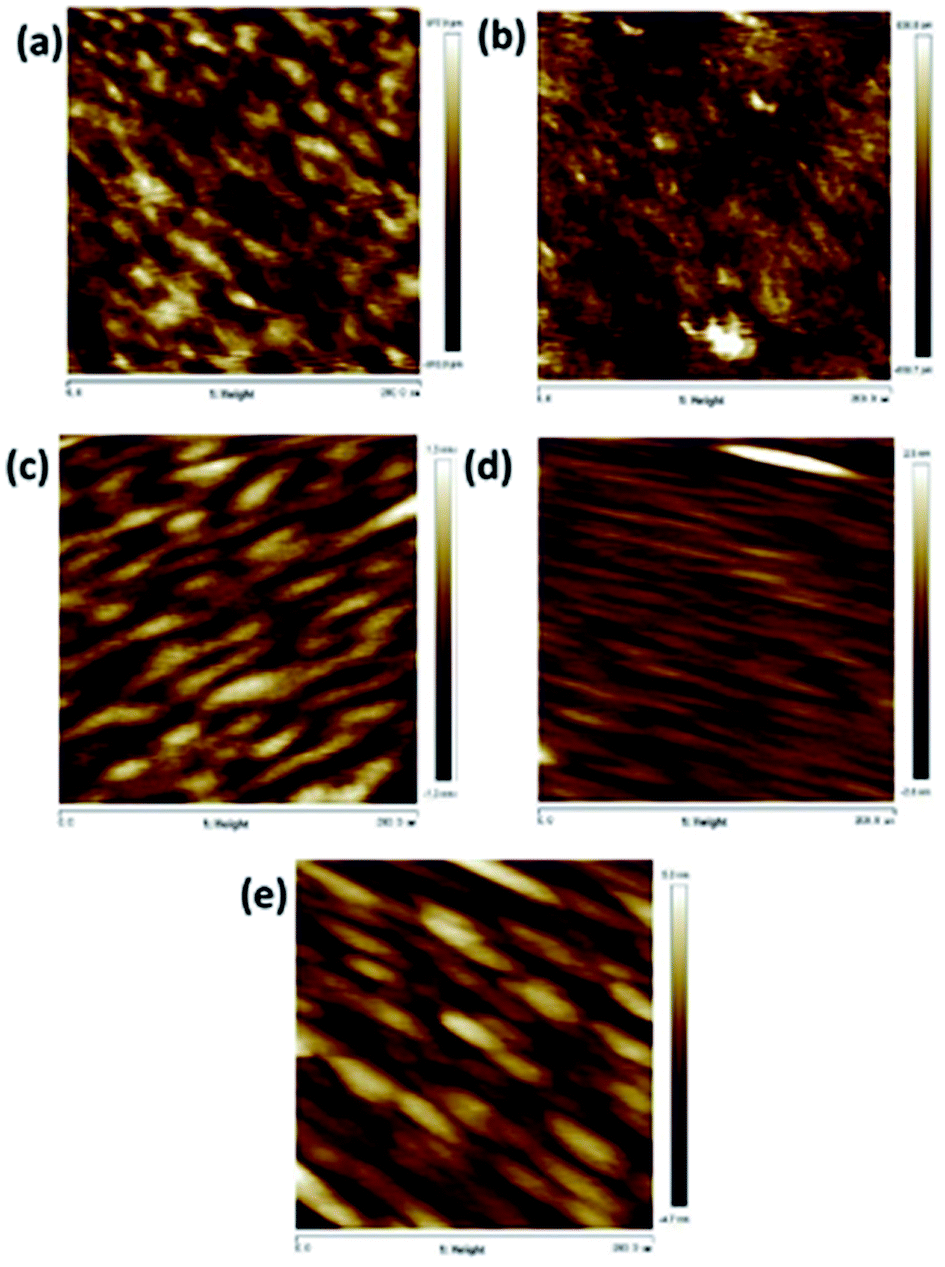 | ||
| Fig. 2 Surface AFM morphologies of MoSx at annealing temperature of (a) 400 °C, Ra = 0.225, (b) 500 °C, Ra = 0.153, (c) 600 °C, Ra = 0.298, (d) 700 °C, Ra = 0.312, (e) 800 °C, Ra = 1.14. | ||
Fig. 3(a)–(e) show the high-resolution XPS energy spectrum under the annealing temperatures of 400 °C, 500 °C, 600 °C, 700 °C, and 800 °C, respectively. The XPS peak fit software was used to fit the curve, obtaining the 3d5/2 and 3d3/2 tracks of Mo 4+, and the energy spectrum corresponding to 3d5/2 and 3d3/2 of Mo 6+ and S 2. From the figures, it could be seen that the MoSx films prepared under different annealing conditions showed two peaks of the 3d track of Mo 4+ around 229.2 eV and 233.0 eV, which corresponded to the 3d5/2 and 3d3/2 binding energy of Mo 4+.13,14 The peaks around 232.4 eV and 236.0 eV belonged to the 3d5/2 and 3d3/2 of Mo 6+.15 There was the peak in the binding energy of 226.3 eV, which corresponded to the S 2s.
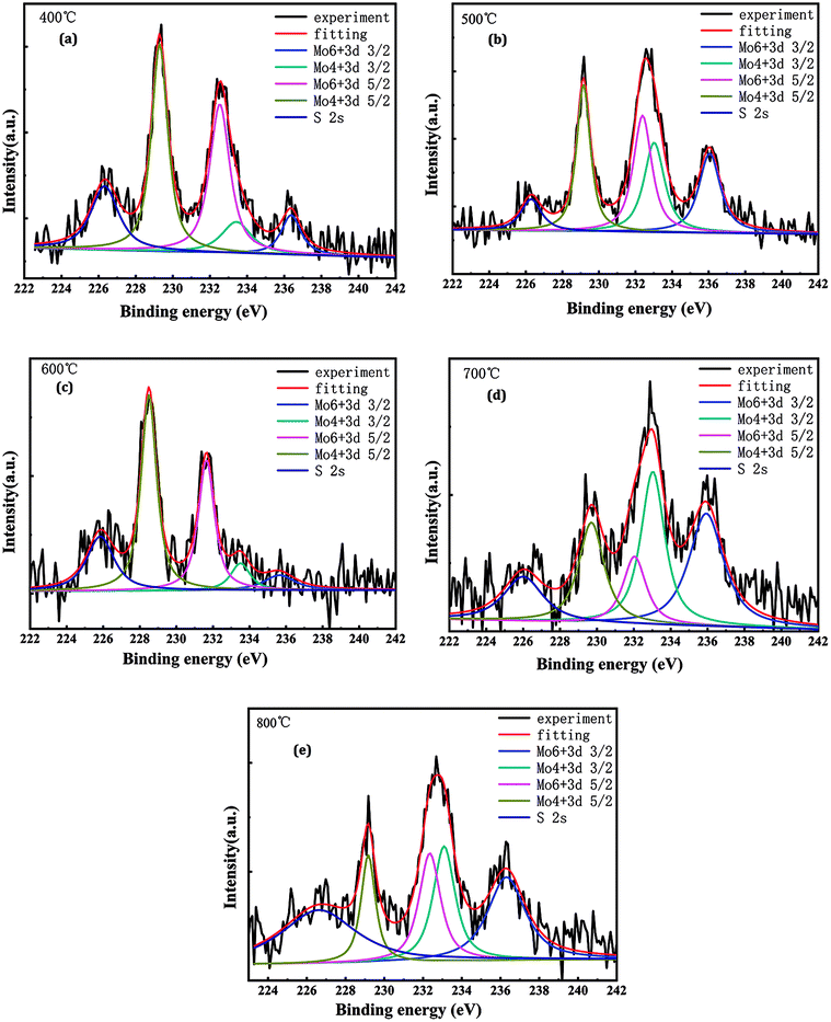 | ||
| Fig. 3 XPS spectra of MoSx film at annealing temperature of (a) 400 °C, (b) 500 °C, (c) 600 °C, (d) 700 °C, (e) 800 °C. | ||
The proportions of Mo in different valence states prepared under different annealing temperatures are listed in Table 1. From the proportions of Mo 6+ and Mo 4+, as the annealing temperature rises, the proportion of Mo 4+ showed a changing trend of decreasing first, then increasing second and decreasing again. It indicates that when the annealing temperature is 400 °C, most of the (NH4)2MoS4 had decomposed into MoSx. As the temperature continued to rise, the oxidation was enhanced, leading to the generation of MoO3. Therefore, when the temperature was 500 °C, the proportion of Mo 4+ decreased and that of Mo 6+ increased. With further increase of the annealing temperature, the lower layer decomposed further, and the probability of MoSx towards oxidation decreases, therefore causing the proportion of the MoSx to increase again. When the annealing temperature rises again, the excessive temperature leads to the loss of the element S, leading to a decrease in the proportion of Mo 4+. As shown by the data in the table, the proportions of 3d3/2 of Mo 6+ and Mo 4+ of the sample at the annealing temperature of 500 °C increased significantly. In addition, the area ratio of the energy spectrum of the tracks of 3d3/2 and 3d5/2 of Mo 6+ of the samples at the annealing temperature of 500 °C was close to 2![[thin space (1/6-em)]](https://www.rsc.org/images/entities/char_2009.gif) :3 and satisfied the Boltzmann distribution rule, which makes the solar cells performance relatively improved. When the annealing temperature was at 700 °C and 800 °C, respectively, the energy spectrum area corresponding to the peak of 3d3/2 of Mo was larger than that corresponding to the 3d5/2, and the particle distribution lost its balance seriously. Moreover, the quality of the film was damaged severely and the performance of the solar cell's components prepared were lowered significantly.
:3 and satisfied the Boltzmann distribution rule, which makes the solar cells performance relatively improved. When the annealing temperature was at 700 °C and 800 °C, respectively, the energy spectrum area corresponding to the peak of 3d3/2 of Mo was larger than that corresponding to the 3d5/2, and the particle distribution lost its balance seriously. Moreover, the quality of the film was damaged severely and the performance of the solar cell's components prepared were lowered significantly.
| Sample | Mo 6+ 3d3/2 (%) | Mo 6+ 3d5/2 (%) | Mo 6+ (%) | Mo 4+ 3d3/2 (%) | Mo 4+ 3d5/2 (%) | Mo 4+ (%) |
|---|---|---|---|---|---|---|
| 400 °C | 9.67 | 36.98 | 46.65 | 11.51 | 41.84 | 53.35 |
| 500 °C | 21.99 | 27.93 | 49.92 | 23.76 | 26.32 | 50.08 |
| 600 °C | 7.64 | 34.21 | 41.85 | 8.54 | 49.61 | 58.15 |
| 700 °C | 33.60 | 13.33 | 46.93 | 31.18 | 21.88 | 53.06 |
| 800 °C | 32.78 | 24.44 | 57.22 | 26.50 | 16.28 | 42.78 |
Fig. 4 shows the high-resolution XPS energy spectrum of the S 2p track of the MoSx film under different annealing temperatures. From the figure, it could be seen that as the temperature rises the XPS spectrum peak of the S 2p track decreases first, then increases and decreases again, which was the same as the changing roles of the Mo 6+ and Mo 4+ proportions.
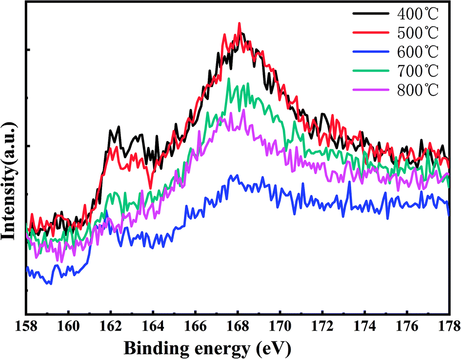 | ||
| Fig. 4 High-resolution XPS energy spectrum of S 2p track of MoSx film under different annealing temperatures. | ||
The spin-coating technique was used to prepare the Ag grid line/ITO/MoSx/p-Si/p+-Si/Ag. As shown by the heterojunction solar cells made from the two-dimensional materials in Fig. 5(a), through the relation analysis between the film structure and photoelectric conversion characteristics, the physical mechanism that limits the improvement of the efficiency of the heterojunction battery was studied. Fig. 5(a) shows the current density–voltage (J–V) curve diagrams of the ITO/MoSx/p-Si/p+-Si/Ag heterojunction solar cells prepared by the MoSx films (which are obtained under different annealing temperatures) under the lighting condition of AM 1.5. The electrical parameters of its solar cell's components are shown in Table 2. As seen from the table, as the annealing temperature of the MoSx film increases, the current density of the short circuit, open-circuit voltage, fill factor and conversion efficiency increase first and then decrease, wherein when the annealing temperature was 500 °C, the photovoltaic performance of the MoSx heterojunction solar cells was superior to the cell performance of the batteries prepared under other conditions. The current density of the short circuit Jsc was the largest, reaching 37.21 mA cm−2, which increased slightly compared with other samples. This may be caused by the fact that the structure of the sample prepared under this condition was in the initial zone from the amorphous to the crystalline transition, the film surface was relatively smooth and the boundary defects of the crystal particles were relatively less, reducing the defect complex of the carrier at the crystal particle boundary, facilitating the transmission of the carrier. The open-circuit voltage (Voc) increased from 154.8 mV to 328.2 mV, and then decreased to 195 mV. This may be caused by the proportion changes of Mo 6+ and Mo 4+. Under this condition, the proportion of Mo 6+ was larger, which increased the built-in electric field and improved the open-circuit voltage. Compared with the heterojunction solar cells prepared under other conditions, the fill factor (FF) had an obvious increase, which could be explained by the fact that under this condition, there was almost no crystal particle boundary due to the relatively smooth film surface, reducing the ohmic shunt loss and increasing the open-circuit voltage and FF factors. Moreover, the distribution of the track particles of the 3d3/2 and 3d5/2 of Mo 4+ was close to the Boltzmann distribution rule, which facilitated the transmission of the carrier and further decreased the serial ohm loss and increased the short-circuit current and FF factors. Moreover, the high-voltage output had a larger current density output. While the temperature rose continuously, at 600 °C, the MoS2 film crystallized gradually, showing a large area of very fine crystal particles and the crystal particle boundary increased. Due to the existence of defects at the crystal particle boundary, the recombination of the carriers at the boundary increased at the defects, which decreased the performance of the heterojunction solar cells. When the temperature rose again, the MoSx film was damaged due to the high temperature. When the temperature reduced to 800 °C, the film showed an abnormal J–V curve and no longer had a photovoltaic performance.
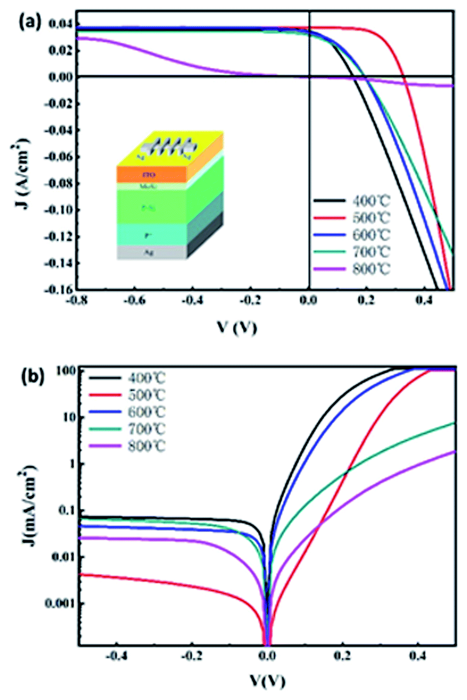 | ||
| Fig. 5 The current density–voltage (J–V) curve diagrams with light (a) and without light (b) of the ITO/MoSx/p-Si/p+-Si/Ag heterojunction solar cells prepared by the MoSx films. | ||
| Sample | Jsc (mA cm−2) | Voc (V) | FF (%) | Eff (%) | n0 | J0 (mA cm−2) | Rs (Ω) | Rsh (Ω) |
|---|---|---|---|---|---|---|---|---|
| 400 °C | 34.67 | 0.1548 | 37.85 | 2.03 | 1.55 | 5.85 × 10⁻⁴ | 2.00 | 56 |
| 500 °C | 37.21 | 0.3282 | 61.80 | 7.55 | 1.10 | 6.17 × 10⁻⁷ | 1.16 | 84 |
| 600 °C | 34 | 0.1946 | 38.12 | 2.52 | 1.57 | 1.32 × 10⁻⁴ | 2.16 | 61 |
| 700 °C | 31.78 | 0.195 | 36.77 | 2.28 | 2.43 | 1.45 × 10⁻⁴ | 2.55 | 67 |
| 800 °C | — | — | — | — | 2.42 | 3.04 × 10⁻⁵ | — | — |
Fig. 5(b) shows the dark-state Ln J–V curve of the heterojunction solar cells prepared by the MoSx film obtained under different annealing temperatures. From the figure, the heterojunction solar cells at the annealing temperature of 500 °C had a better rectification ratio. After the formula computing,
 | (2) |
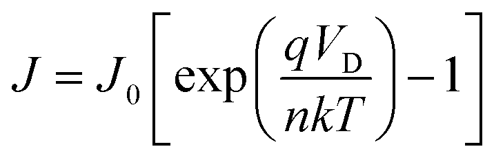
Fig. 6 shows the EQE spectrum of ITO/MoSx/p-Si/p+-Si/Ag heterojunction solar cells prepared by the MoSx films under different annealing temperatures. From the figure, the response within the short wave of the EQE of the heterojunction solar cells prepared at the annealing temperature of 400 °C was lower, while that within the long wave scope increased. This was because the film grew under the lower temperature while in an amorphous state, but the total spectral response was relatively low. The total spectral response of the solar cells under the annealing temperature of 500 °C increased relatively, but as the annealing temperature rose, the spectral response decreased to some extent. This was consistent with the result that the short-circuit current of the heterojunction solar cells under the annealing temperature of 500 °C in the J–V curve was relatively higher.
 | ||
| Fig. 6 The EQE spectrum of ITO/MoS2/p-Si/p+-Si/Ag heterojunction solar cells. | ||
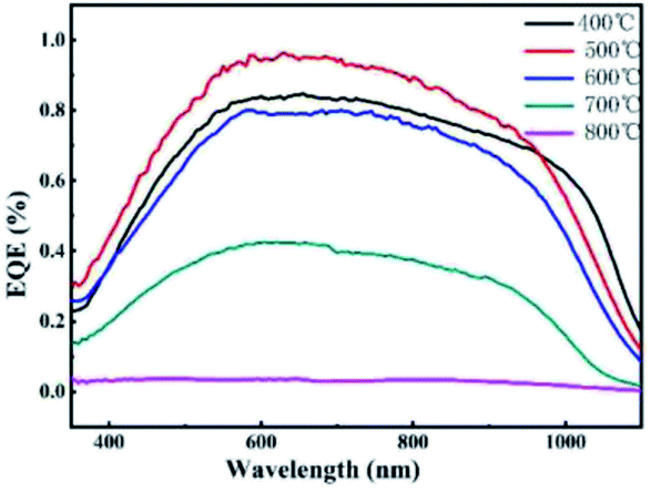
Fig. 7(a) shows the C–V curve of different-annealing-temperatures' heterojunction solar cells which the test frequency is 100 kHz. Fig. 7(b) shows the C−2–V curve calculated from the C–V curve. It can be seen that the C−2–V curves of the heterojunction solar cells prepared under all conditions were in a good linear distribution and corresponded to the nature of abrupt junction. The impurity concentration (NB) and built-in voltage (Vbi) of the MoSx films were calculated according to the slope of the fitting straight-line of C−2–V. When V = 0, the values of the impurity concentration and width of the depletion area are shown in Table 2.
 | ||
| Fig. 7 The C–V curve measured under the frequency of 100 kHz of the heterojunction solar cells (a) and the C−2–V curve calculated from C–V curve (b). | ||
Table 3 indicates that as the annealing temperature increases, the built-in voltage of the heterojunction solar cells prepared, increased first and then decreased. The built-in voltage of the heterojunction solar cells prepared under the annealing temperature of 500 °C was the maximum and its open-circuit voltage was also the maximum, which are consistent with the results measured by the light J–V curve. With the increase in the annealing temperature, the impurity concentration of the heterojunction battery prepared also increased first and then decreased. The width of the corresponding depletion area decreased first, then increased and decreased again. The width of the depletion area of the heterojunction solar cells prepared under the annealing temperature of 500 °C was smaller, but the impurity concentration of the space charge region of the heterojunction formed was the largest, so the formed built-in electric field was the largest, leading to a maximum of the open-circuit voltage. This may be caused by the change in the proportion of Mo 6+ and Mo 4+ under this condition, leading to the change in the energy band structure of the samples. When the annealing temperature was 700 °C and 800 °C, the impurity concentration of the space charge region of the heterojunction decreased and the width of its depletion area also decreased. Therefore, the built-in voltage decreased significantly.
| Sample | Vbi (V) | NB (cm−3) | W (nm) |
|---|---|---|---|
| 400 | 0.50 | 1.96 × 10¹⁵ | 812 nm |
| 500 | 0.72 | 2.728 × 10¹⁵ | 545 nm |
| 600 | 0.46 | 1.59 × 10¹⁵ | 572 nm |
| 700 | 0.37 | 1.23 × 10¹⁵ | 533 nm |
| 800 | 0.32 | 1.44 × 10¹⁵ | 520 nm |
4. Conclusions
In conclusion, we found the optimal annealing temperature condition for the growth of the MoSx film on a silicon substrate. The research results suggested that for the samples prepared under different annealing temperatures, the degree of order of the film at 500 °C was enhanced, and it was in the initial zone from the amorphous to the microcrystal phase change, and the proportion of Mo 6+ was relatively enhanced. When the temperature continued to rise, the intergranular defects increased and the overall degree of the order of the film decreased. As the temperature rose, the current density of the short circuit, open-circuit voltage, fill factor and conversion efficiency increased first and then decreased. When the annealing temperature was 500 °C, the performance of the solar cells was optimal, the current density of the short circuit (Jsc) reached 37.21 mA cm−2, the open-circuit voltage (Voc) increased to 32.82 mV, the fill factor was 61.8% and the conversion efficiency of the solar cells reached 7.55%. The films under this condition were in the initial zone from the amorphous to the crystalline transition, and the film surface was relatively smooth, reducing the defect complex of the carrier at the boundary of the crystal particles. Moreover, the track particle distribution of the 3d3/2 and 3d5/2 of Mo 4+ was closer to the Boltzmann distribution rule. All the above conditions reduce the serial ohmic losses and improve the short-circuit current and FF factors of the solar cells to some extent. Under this condition, the proportion of Mo 6+ reaches the maximum, improving the open-circuit voltage to some extent. Meanwhile, the reduction of the ohmic shunt loss enhances the open-circuit voltage of the solar cells, makes a larger contribution to the improvement of the fill factor and makes the output of the high voltage have a larger current density output.Conflicts of interest
There are no conflicts to declare.Acknowledgements
This work was supported by the Research Funds for the Hebei Universities (041300119001).Notes and references
- M.-L. Tsai, S.-H. Su, J.-K. Chang, D.-S. Tsai, C.-H. Chen, C.-I. Wu., L.-J. Li, L.-J. Chen and J.-H. He, ACS Nano, 2014, 8, 8317–8322 CrossRef CAS
.
- J. Bae, M. K. Song, Y. J. Park, J. M. Kim, M. Liu and Z. L. Wang, Angew. Chem., Int. Ed., 2011, 50, 1683–1687 CrossRef CAS
- S. Z. Butler, S. M. Hollen, L. Cao., Y. Cui, J. A. Gupta, H. R. G. Rrez, T. F. Heinz, S. S. Hong, J. Huang, A. F. Ismach, E. Johnston-Halperin, M. Kuno, V. V. Plashnitsa, R. D. Robinson, R. S. Ruoff, S. Salahuddin, J. Shan, L. Shi, M. G. Spencer, M. Terrones, W. Windl and J. E. Goldberger, ACS Nano, 2013, 7, 2898–2926 CrossRef CAS
- A. O'Neill, U. Khan, P. N. Nirmalraj, J. Boland and J. N. Coleman, J. Phys. Chem. C, 2011, 115, 5422–5428 CrossRef
- Q. Ji, Y. Zhang, T. Gao, Y. Zhang, D. Ma, M. Liu, Y. Chen, X. Qiao, P. H. Tan, M. Kan, J. Feng, Q. Sun and Z. Liu, Nano Lett., 2013, 13, 3870–3877 CrossRef CAS
- J. N. Coleman, M. Lotya, A. O'Neill, S. D. Bergin, P. J. King, U. Khan, K. Young., A. Gaucher, S. De., R. J. Smith, I. V. Shvets, S. K. Arora, G. Stanton, H.-Y. Kim., K. Lee, G. T. Kim., G. S. Duesberg, T. Hallam., J. J. Boland, J. J. Wang., J. F. Donegan, J. C. Grunlan, G. Moriarty, A. Shmeliov, R. J. Nicholls, J. M. Perkins, E. M. Grieveson, K. Theuwissen, D. W. McComb, P. D. Nellist and V. Nicolosi, Science, 2011, 331, 568–571 CrossRef CAS
- G. Eda, H. Yamaguchi, D. Voiry, T. Fujita, M. Chen and M. Chhowalla, Nano Lett., 2011, 11, 5111–5116 CrossRef CAS
- Z. Zeng, Z. Yin, X. Huang, H. Li, Q. He, G. Lu, F. Boey and H. Zhang, Angew. Chem., Int. Ed., 2011, 50, 11093–11097 CrossRef CAS
- M. A. Khan, R. Kurchania, S. Corkovic, Q. Zhang and S. J. Milne, Mater. Lett., 2006, 60, 1463–1465 CrossRef CAS
- S. Mohammadi, H. Abdizadeh and M. R. Golobostanfard, Ceram. Int., 2013, 39, 6953–6961 CrossRef CAS
- N. Zheng, Z. Wang, K. Zhang, Y. Li, F. Huang and Y. Cao, J. Mater. Chem. A, 2019, 7, 1429–1434 RSC
- S. Takenaka and H. Kozuka, Appl. Phys. Lett., 2001, 79, 3485–3487 CrossRef CAS
- K. K. Liu, W. Zhang, Y. H. Lee, Y. C. Lin, M. T. Chang, C. Y. Su, C. S. Chang, H. Li, Y. Shi, H. Zhang, C. S. Lai and L. J. Li, Nano Lett., 2012, 12, 1538–1544 CrossRef CAS
- L. Liu, Y. Jiao, C. Gao, H. Xu, W. Zhao, W. Dai, W. Yu and X. Li, J. Alloys Compd., 2018, 738, 158–163 CrossRef CAS
- A. S. George, Z. Mutlu, R. Ionescu, R. J. Wu., J. S. Jeong, H. H. Bay, Y. Chai, K. A. Mkhoyan, M. Ozkan and C. S. Ozkan, Adv. Mater., 2014, 24, 7461–7466 CAS
| This journal is © The Royal Society of Chemistry 2019 |