
 Open Access Article
 This Open Access Article is licensed under a Creative Commons Attribution-Non Commercial 3.0 Unported Licence
Bidirectional heterostructures consisting of graphene and lateral MoS2/WS2 composites: a first-principles study†
Yingqi Tang‡
a,
Hao Li‡b,
Xiaotong Maoa,
Ju Xie c,
Jin Yong Lee*b and
Aiping Fu*a
c,
Jin Yong Lee*b and
Aiping Fu*a
aCollege of Chemistry and Chemical Engineering, State Key Laboratory of Bio-Fibers and Eco-Textiles, Qingdao University, Qingdao 266071, China. E-mail: apfu@qdu.edu.cn; lxylhlfap@163.com; Fax: +86-531-85950768; Tel: +86-532-85950767
bDepartment of Chemistry, Sungkyunkwan University, Suwon 16419, Korea. E-mail: jinylee@skku.edu; Fax: +82-031-290-7075; Tel: +82-031-299-4560
cCollege of Chemistry and Chemical Engineering, Yangzhou University, Yangzhou 225002, China
First published on 29th October 2019
Abstract
First-principles calculations have been performed to explore the structural and electronic properties of bidirectional heterostructures composed of graphene and (MoS2)X/(WS2)4−X (X = 1, 2, 3) lateral composites and compare them with those of heterobilayers formed by graphene and pristine MS2 (M = Mo, W). The band gaps of the lateral heterostructures lie between those of pristine MoS2 and WS2. The weak coupling between the two layers can induce a tiny band-gap opening of graphene and formation of an n-type Schottky contact at the G-(MoS2)X/(WS2)4−X interface. Moreover, the combination ratio of MoS2/WS2 can control the electronic properties of G-(MoS2)X/(WS2)4−X. By applying external electric fields, the band gaps of (MoS2)X/(WS2)4−X (X = 0, 1, 2, 3, 4) monolayers undergo a direct–indirect transition, and semiconductor–metal transitions can be found in WS2. External electric fields can also be used effectively to tune the binding energies, charge transfers, and band structures (the types of Schottky and Ohmic contacts) of G-(MoS2)X/(WS2)4−X heterostructures. These findings suggest that G-(MoS2)X/(WS2)4−X heterostructures can serve as high-performance nano-electronic devices.
1. Introduction
Graphene has been used widely in various fields owing to its electronic, mechanical, and optical properties since it was discovered in 2004.1,2 However, the zero gap of graphene limits its development and applications.3 A vertical heterostructure formed by graphene and other two-dimensional matter, e.g., hexagonal boron nitride or transition-metal dichalcogenides (TMDs), via van der Waals forces is a promising method of solving this problem because it could lead to a band-gap opening while preserving the mechanical and electronic structures of graphene.2–19 Most TMDs, of which the general chemical formula is MX2 (M = Mo, W, V, Co etc., X = S, Se, or Te, etc.), are promising candidates for electronic devices because they have a direct band gap, high carrier mobility, high on/off current ratios, and unique exaction properties.2,6,12,16–24 Vertical heterostructures composed of a pristine TMDs monolayer and graphene have been the subject of extensive investigation.2,10,12–16,19,25–28Lateral heterostructures have been fabricated within TMD monolayers (MoS2/WS2, WS2/WSe2, MoSe2/WSe2, etc.) and have opened up unprecedented opportunities to improve the performance of electronic devices with tunable electronic properties.2,29–34 However, due to limitations of the experimental techniques, the electrochemical properties of such in-plane heterostructures have not been fully explored. Although theoretical studies have reported the electronic properties of some lateral heterostructures,24,35–39 the effects of the component ratio and external electric fields on the properties of such hybrid systems remain unclear. We are left with an interesting question: would any peculiar properties appear in the vertical and lateral combined bidirectional heterostructures formed by graphene and in-plane TMDs composites in comparison with the heterobilayer from graphene and pristine TMDs?
Although extraordinary bidirectional heterostructures of γ-graphyne-MoSe2/WSe2 were investigated by Sun et al.,35 the G-MoS2/WS2 system has not been studied. Inspired by the above factors, bidirectional heterostructures formed by graphene and lateral MoS2/WS2 composite are explored here on the basis of first-principles calculations. For comparison purposes, the heterobilayers from graphene and pristine MoS2 or WS2 are also considered. Because previous research has demonstrated that external electric fields can be used to tune the band gaps or other electronic structures of vertical heterostructures,9,10,15,17–19,27,28,40–45 the structural and electronic properties of a (MoS2)X/(WS2)4−X, (X = 0, 1, 2, 3, 4) monolayer with different proportions and vertical heterobilayers with graphene under external electric fields are systematically investigated by density functional theory (DFT) calculations. The results indicate that external electric fields can induce consequential changes in the properties of a (MoS2)X/(WS2)4−X monolayer and G-(MoS2)X/(WS2)4−X heterostructures.
2. Computational methods
The DMol3 code was used for geometric optimization and electronic properties calculations.46,47 The generalized gradient approximation (GGA) with a Perdew–Burke–Ernzerhof (PBE) functional and the DFT semi-core pseudo-potentials (DSPP) double numerical atomic basis set plus polarization (DNP) were employed.48 To show the expected differences with the different function, the on-site Coulomb interaction (GGA + U approach) was adopted to study the electric properties using Vienna ab initio simulation package program (VASP) package.49,50 Due to the poor description of the weak van der Waals interactions of the popular PBE functional,56 an empirical dispersion-corrected density functional theory approach proposed by Grimme was used.51 The optimal geometric convergence criteria of energy, force, and displacement were 1.0 × 10⁻⁵ Ha, 0.002 Ha Å−1, and 0.005 Å, respectively. The K-point was set to 9 × 9 × 1 for structural optimization and to 15 × 15 × 1 to calculate electronic properties. The vacuum thickness was set to more than 20 Å to avoid interactions between the neighboring layers. A vertical external electric field in the range of 0 to 1.0 V Å−1 was applied to (MoS2)X/(WS2)4−X lateral heterostructures and −1.0 to 1.0 V Å−1 to the G-(MoS2)X/(WS2)4−X heterobilayer, with a positive electric field pointing from (MoS2)X/(WS2)4−X to graphene and a negative field pointing in the reverse d direction.39,41 Electron density differences were computed by CASTEP code.52The optimized lattice constants of graphene, MoS2, and WS2 were 2.472 Å, 3.214 Å, and 3.206 Å, respectively. In line with the modeling methods of graphene-MoS2,16,45 silicene-MoS2,44 and germanene-MoS2 heterostructures,43,53 a 4 × 4 substrate layer of (MoS2)X/(WS2)4−X was chosen to match the 5 × 5 graphene monolayer, producing a tolerable lattice mismatch for this system (∼4.0%). To quantitatively describe the interaction strength between the graphene sheet and the (MoS2)X/(WS2)4−X monolayer, the binding energies were defined as
| Eb=(Etotal − E(MoS2)X/(WS2)4−X − Egraphene)/N |
3. Results and discussion
3.1. (MoS2)X/(WS2)4−X monolayer
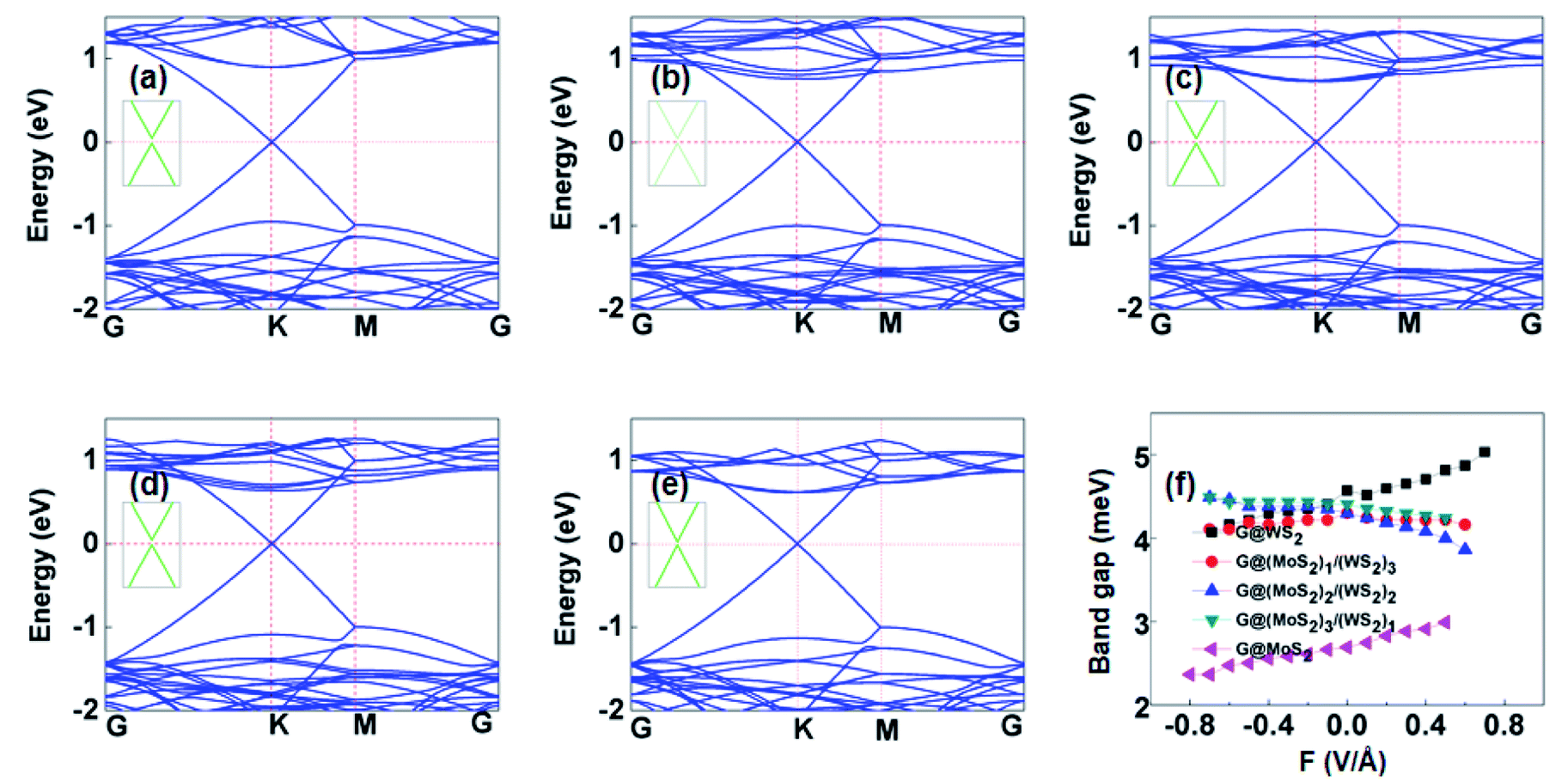
The electronic properties of pristine MoS2 or WS2 and the (MoS2)X/(WS2)4−X lateral heterostructures systems illustrated in Fig. 1, i.e., (MoS2)1/(WS2)3, (MoS2)2/(WS2)2, and (MoS2)3/(WS2)1, were examined first. Fig. 2 presents the calculated electronic band structures of G-(MoS2)X/(WS2)4−X heterostructures. As shown in Fig. 2, pristine MoS2 and WS2 (x = 0 and 4) have respective direct band gaps at the K point of 1.59 eV and 1.81 eV, which are almost identical to previously reported values.22,36,37,45 The band gaps of the hybrid lateral heterostructures with different combination MoS2/WS2 ratios lie between those of pristine MoS2 and WS2, and they all maintain the direct band gaps of a pristine TMDs monolayer.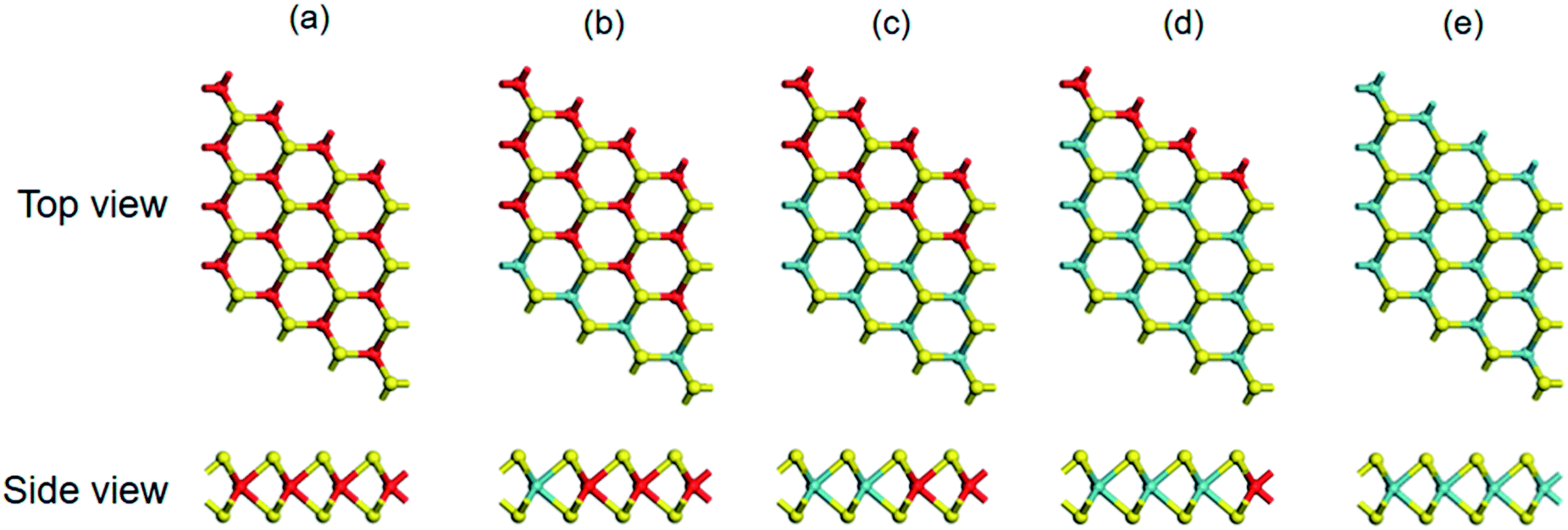 | ||
| Fig. 1 Top and side views of stable configurations of WS2 (a), (MoS2)1/(WS2)3 (b), (MoS2)2/(WS2)2 (c), (MoS2)3/(WS2)1 (d), MoS2 (e), respectively. The yellow, green, and red balls denote S, Mo and W atoms, respectively. | ||
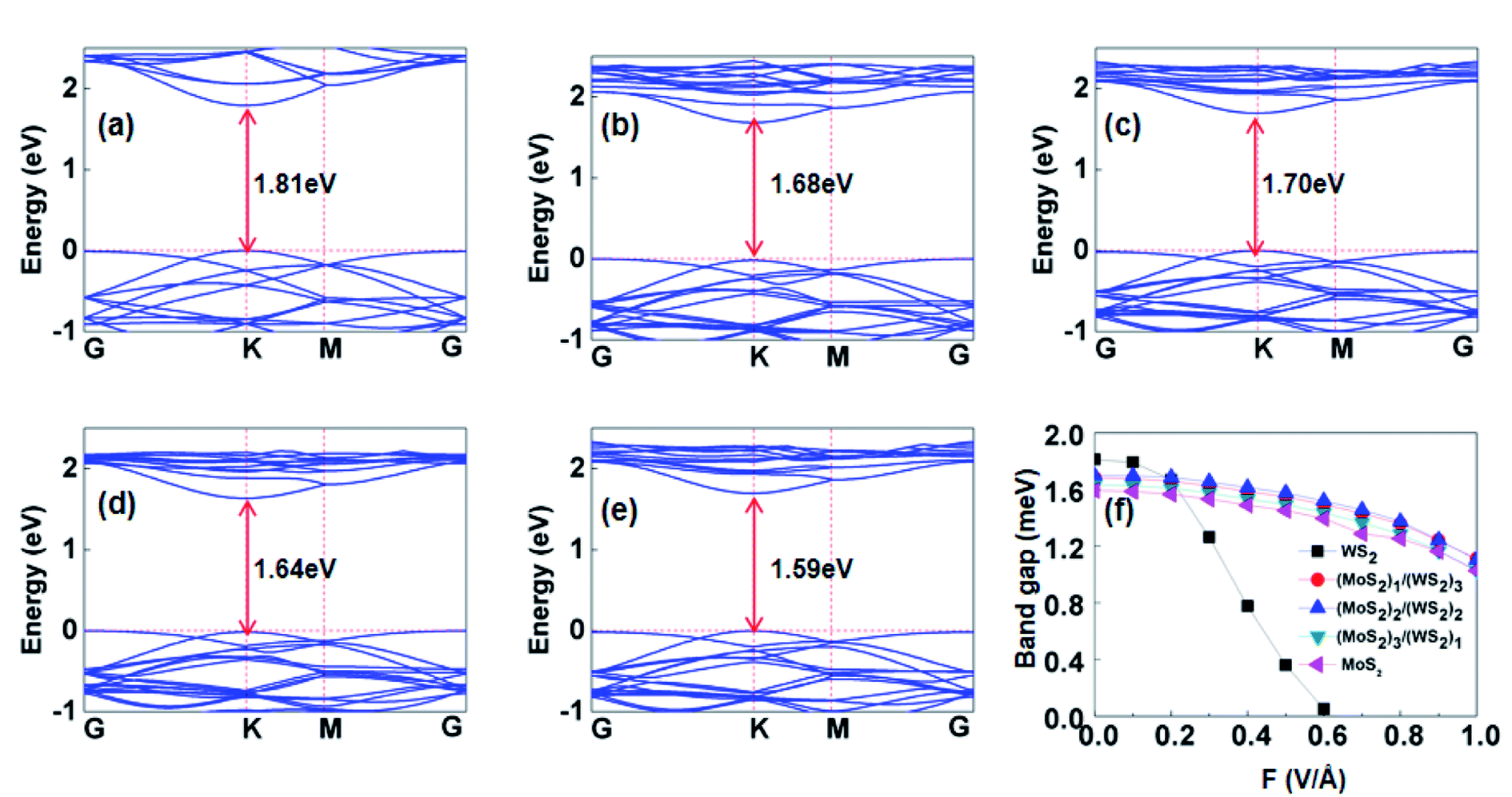 | ||
| Fig. 2 Band structures of WS2 (a), (MoS2)1/(WS2)3 (b), (MoS2)2/(WS2)2 (c), (MoS2)3/(WS2)1 (d), and MoS2 (e), respectively. The horizontal red lines represent the Fermi level. (f) Calculated band gap of (MoS2)X/(WS2)4−X monolayer as a function of electric field intensity. | ||
Although some theoretical studies of MoS2/WS2 lateral heterostructures have been reported in recent years,24,35–38 the effects of external electric fields on the electronic properties of this lateral hybrid monolayer have been ignored. As the external electric field varies from 0 to 0.6 V Å−1, the bond distance of WS2 monolayer increases with the electric field strength. And the bond distance decreases when the electric field strength more than 0.7 V Å−1. The bond distance of MoS2 was also increases with the electric field strength, but the change is weak (<0.1 Å). The change of bond distance of the lateral hybrid (MoS2)X/(WS2)4−X (X = 1, 2, 3) heterostructures are not obvious. As shown in Fig. 2, the applied electric fields are associated with a decreasing trend in band gaps for the above systems because field-induced repulsion among the electronic levels results in a shift in conduction band minimum (CBM) toward the Fermi level (EF), consequently, a reduction in band gaps (Fig. S1† and 2).
Furthermore, a direct–indirect band gap transition of (MoS2)X/(WS2)4−X (X = 0, 1, 2, 3, 4) under vertical electric fields has also been observed. The pristine MoS2 and (MoS2)X/(WS2)4−X lateral heterostructures maintain semiconductor characteristics under an external electric field (F ≤ 1.0 V Å−1). While for WS2, the conduction band overlaps the valence band across the Fermi level at 0.6 V Å−1 to 0.7 V Å−1 (Fig. S1†), and the band gap of WS2 shows a semiconductor–metal transition, which is consistent with a report by Affandi.54 As shown in Fig. S1,† the band structures of MoS2 are more stable than that of WS2 under the external electronic fields with different intensity. We suspect that the 5d electrons of W may cross the Fermi level under the strong electric field, which would cause the materials to be metallic. This is in good agreement with previous studies.20,25,54 As a result, the electric properties of (MoS2)X/(WS2)4−X monolayer with high W concentration become not stable under the electric field and present different trend.
3.2. G-(MoS2)X/(WS2)4−X heterostructures
Vertical hybrid structures of graphene stacked on a (MoS2)X/(WS2)4−X monolayer were constructed and calculated. A supercell is formed by alternate stacking of graphene sheets on a (MoS2)X/(WS2)4−X monolayer, with 16 metal (Mo or W) atoms, 32 S atoms, and 50 C atoms. To analyze the optimal stacking patterns, two representative approaching modes were considered. The C atom was placed on top of the metal atoms (W or Mo) or was located above the top of the S atoms (Fig. S2†). The binding energies for different stacking patterns differ by less than 0.1 meV per C atom. This indicates that interlayer bonding takes place irrespective of stacking pattern, which is in agreement with G-MoS2 and Si-MoS2.16,44 Only the most stable configuration shown in Fig. 3 is considered in the following discussions. The interlayer distances between a (MoS2)X/(WS2)4−X (X = 0, 1, 2, 3, 4) monolayer and graphene are ∼3.2 Å, which suggests that the coupling between them is dominated by van der Waals forces. Graphene exhibits a small wrinkle (∼0.1 Å) in its planar atomic framework for all G-(MoS2)X/(WS2)4−X heterostructures, similar to the previous calculation.16,26,55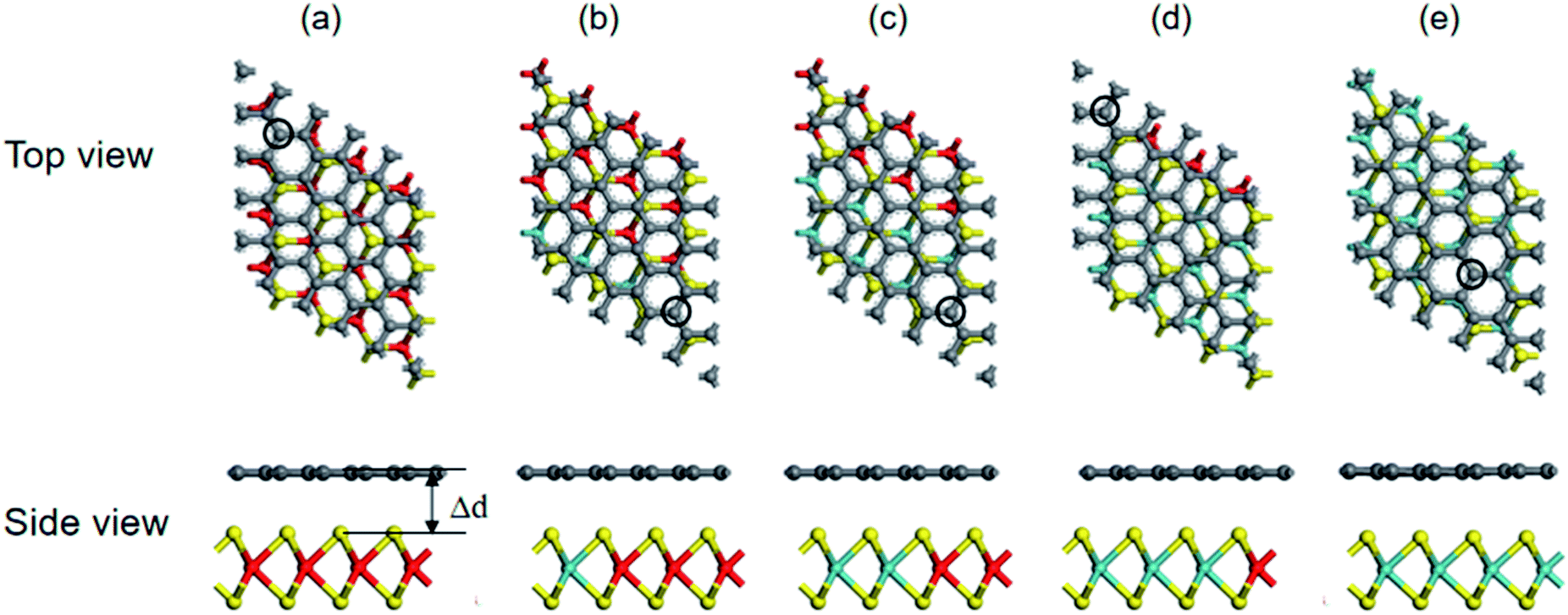 | ||
| Fig. 3 Top and side views of stable configurations of G-WS2 (a), G-(MoS2)1/(WS2)3 (b), G-(MoS2)2/(WS2)2 (c), G-(MoS2)3/(WS2)1 (d), G-MoS2 (e), respectively. The gray balls denote C atom. | ||
Fig. 4 shows the calculated Eb values of G-(MoS2)X/(WS2)4−X (X = 0, 1, 2, 3, 4) heterobilayers. The calculated Eb of G-WS2 is −26.9 meV per C atom, which is nearly identical to previously reported values based on the GGA-PBE function (−26.8 meV and −29 meV).15,55 The Eb of G-MoS2 is −10.2 meV per C atom, which is smaller than the value (−23 meV) reported by Ma et al. based on local density approximation (LDA) calculations,16 which is not surprising given that the LDA method overestimates the calculated results. The binding energies of graphene with (MoS2)1/(WS2)3, (MoS2)2/(WS2)2, and (MoS2)3/(WS2)1 lateral heterostructures were −24.1, −18.9, and −14.4 meV, respectively. This clearly shows that the Eb between graphene and the lateral hybrid MoS2/WS2 with different mixing proportions lies between those of graphene with pristine MoS2 or WS2. As expected, binding strength increases with proportion of WS2 units in (MoS2)X/(WS2)4−X, in the order of G-WS2 > G-(MoS2)1/(WS2)3 > G-(MoS2)2/(WS2)2 > G-(MoS2)3/(WS2)1 > G-MoS2. These Eb values confirm weak van der Waals interactions between the graphene sheet and the (MoS2)X/(WS2)4−X monolayer, including pristine MX2 and hybrid lateral heterostructures. As shown in the Fig. S3,† the d band of MoS2 has much sharper peak than WS2 around the Fermi level, indicating that the 4d electrons of Mo atoms are more localized than the 5d electrons of W atoms. The more delocalized 5d orbitals leads to the enhancement of interlayer coupling with the concentration of W increases, and consequently results in the strengthen of binding energy.
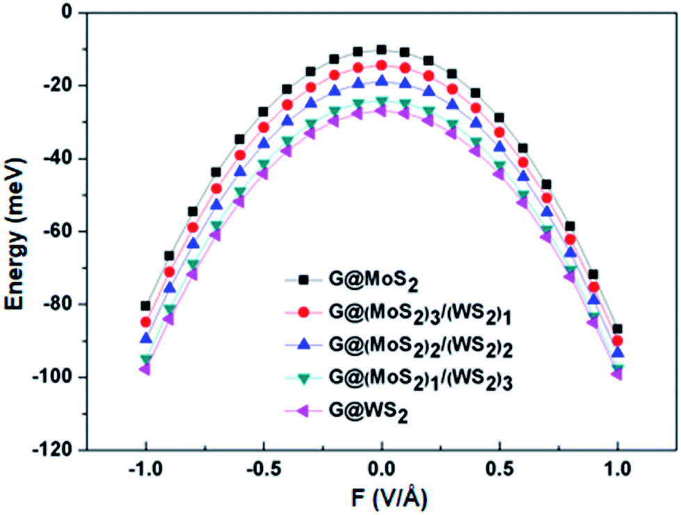 | ||
| Fig. 4 Binding energies (Eb) as a function of the electric field intensity for graphene-(MoS2)X/(WS2)4−X (X = 0, 1, 2, 3, 4) heterobilayers. | ||
To probe the effect of external electric fields on the interaction strength of G-(MoS2)X/(WS2)4−X heterostructures, vertical electric fields in the range of −1.0 V Å−1 to 1.0 V Å−1 were applied to the heterobilayer. The computed Eb as a function of electric fields for G-(MoS2)X/(WS2)4−X (X = 0, 1, 2, 3, 4) is plotted in Fig. 4. The stability order of the heterostructures was maintained regardless of electric field intensity. An applied positive or negative electric field can result in a more negative Eb for the above systems, which suggests that the external electric field can intensify the interaction between the layers and enhance heterobilayer stability. Moreover, the direction of the electric field has a weak influence on Eb, with the effect of the positive field being slightly more pronounced. For G-(MoS2)X/(WS2)4−X heterobilayers, the change of bond length and the interlayer distance are both less than 0.1 Å under the external electric field. So, there is no obvious structural changes in the heterobilayers under the external electric field. Enhancement of interlayer binding in the heterostructures can be attributed to built-in electric fields that are asymmetrical in the sense that graphene and the (MoS2)X/(WS2)4−X monolayer have different electron affinities. Field-driven charge transfer among the component layers then enhances the electrostatic interaction between heterobilayers.
To further explore the bonding nature of graphene and the (MoS2)X/(WS2)4−X monolayer, the charge density difference of the G-(MoS2)X/(WS2)4−X hybrid systems, indicated in Fig. 5(a–e), was used to visualize electron transfer upon formation of the interlayer. This can be defined as
| Δρ = ρtotal − ρ(MoS2)X/(WS2)4−X − ρgraphene |
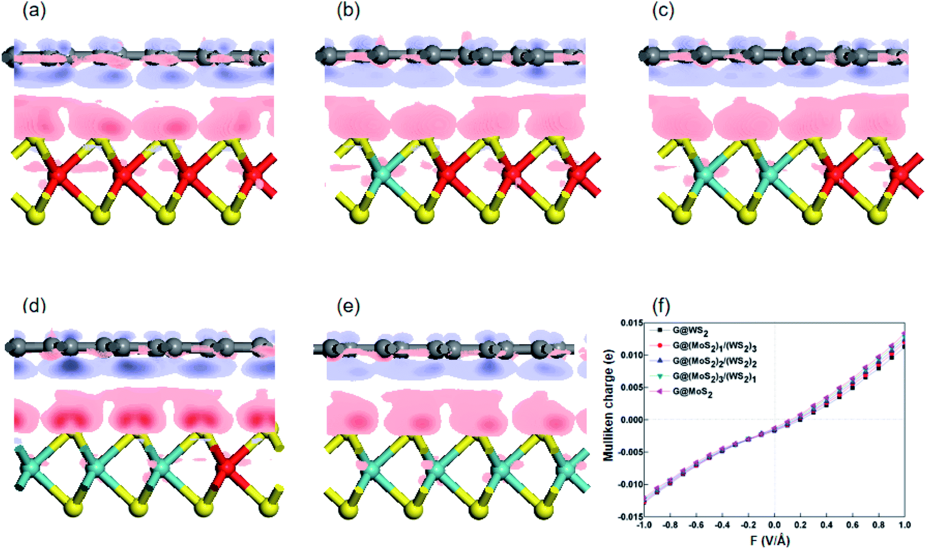 | ||
| Fig. 5 Differential electron density of G-WS2 (a), G-(MoS2)1/(WS2)3 (b), G-(MoS2)2/(WS2)2 (c), G-(MoS2)3/(WS2)1 (d), and G-MoS2 (e), respectively. Pink and blue areas correspond to the accumulation and depletion of electronic densities. (f) Mulliken populations of per C atom in graphene for (MoS2)X/(WS2)4−X as a function of the electric field strength. | ||
The effect of the external electric field on charge redistribution among the G-(MoS2)X/(WS2)4−X interlayers was further examined. Fig. 5f displays the average Mulliken population per C atom in graphene as a function of electric field strength. The extent of charge transfer is in the order of G-WS2 < G-(MoS2)1/(WS2)3 < G-(MoS2)2/(WS2)2 < G-(MoS2)3/(WS2)1 < G-MoS2 regardless of field strength and direction. The negative electric fields cause more electrons to flow from (MoS2)X/(WS2)4−X to graphene; thus, the graphene monolayer is more negatively charged with increasing field intensity. When the electric field reaches −1.0 V Å−1, the graphene in G-WS2, G-(MoS2)1/(WS2)3, G-(MoS2)2/(WS2)2, G-(MoS2)3/(WS2)1, and G-MoS2 gains 0.0128 e, 0.0127 e, 0.0124 e, 0.0123 e, and 0.0121 e per C atom, respectively. When the external electric field is applied in the positive direction, the heterostructures exhibit the opposite response: the transferred electrons of G-WS2 gradually decrease to zero at 0.2–0.3 V Å−1, while other G-(MoS2)X/(WS2)4−X hybrid systems reach zero at 0.1–0.2 V Å−1. A further increase in the strength of the electric field alters the transferred direction of electrons from graphene to the (MoS2)X/(WS2)4−X monolayer, with graphene being more positively charged. In brief, graphene sheets lose electrons as the electric field changes from negative to positive, reaching 0.0113 e, 0.0120 e, 0.0124 e, 0.0129 e, and 0.0134 e per C atom at F = 1.0 V Å−1 for G-WS2, G-(MoS2)1/(WS2)3, G-(MoS2)2/(WS2)2, G-(MoS2)3/(WS2)1, and G-MoS2, respectively.
The degree of charge transfer between heterobilayers can reflect variation in the interface dipole and the magnitude of the band gap opening. To analyze the impact of the weak van der Waals forces between the interlayer on the band gaps of the hybrid G-(MoS2)X/(WS2)4−X heterostructures, the calculated gaps are presented in Fig. 6(a–e). Small band gap openings of 4.6, 4.3, 4.3, 4.4, and 2.7 meV for respective stable heterostructures of G-WS2, G-(MoS2)1/(WS2)3, G-(MoS2)2/(WS2)2, G-(MoS2)3/(WS2)1, and G-MoS2 were observed. The derived gaps of G-WS2 and G-MoS2 are consistent with previously reported results (3.9 meV for WS2, 2 meV for MoS2),16,26 indicating the plausibility of our calculated results. As shown in Fig. S4,† the band structure which used the on-site Coulomb interaction (GGA + U approach) is same to our result in current research. And the difference of band gap is small (2 meV). So, our results are credible. Fig. 6(a–e) shows that the Dirac point of graphene around the Fermi level is well preserved in the band structure of all G-(MoS2)X/(WS2)4−X heterostructures, which suggests a high carrier mobility of the hybrid systems. As shown in Fig. 6f, when an external electric field is applied, the band gaps at the Dirac point of graphene change only slightly (<0.5 meV) in those heterobilayers, regardless of the field direction.
 | ||
| Fig. 6 Band structures of G-WS2 (a), G-(MoS2)1/(WS2)3 (b), G-(MoS2)2/(WS2)2 (c), G-(MoS2)3/(WS2)1 (d), and G-MoS2 (e), respectively. The insets in figure are a magnification of the area near the linear dispersion band at the K point. The horizontal red lines represent the Fermi level. (f) Band gaps of G-(MoS2)X/(WS2)4−X heterostructures as a function of the electric field intensity. | ||
External electric fields have a large effect on the Schottky barrier of the G-(MoS2)X/(WS2)4−X heterostructures in our calculations. When the Fermi level is close to the CBM, known as the n-type Schottky barrier (ΦBn), it is defined as ΦBn = EC − EF. Similarly, the p-type Schottky contact corresponds to the Fermi level close to the valence band maximum (VBM), and the Schottky barrier (ΦBp) is defined as ΦBp = EF − EV, where EV and EF are the CBM and VBM, respectively. The Fermi level was referenced at 0 eV. To quantitatively characterize regulation of the external electric field on the Schottky barrier of the above heterobilayers, the evolutions of Schottky contact type and Schottky barrier height of G-(MoS2)X/(WS2)4−X heterostructures as a function of electric field intensity are supplied in Fig. 7(fa–e). The corresponding band structures of G-(MoS2)X/(WS2)4−X heterostructures under external electric fields at 1.0, −0.5, 0.5 and 1.0 V Å−1 are also shown.
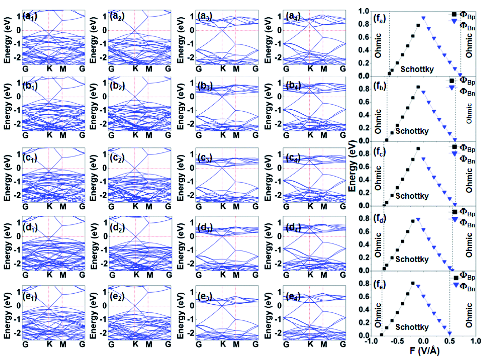 | ||
| Fig. 7 Band structures of G-WS2 (a1−4), G-(MoS2)1/(WS2)3 (b1−4), G-(MoS2)2/(WS2)2 (c1−4), G-(MoS2)3/(WS2)1 (d1−4) and G-MoS2 (e1−4) under electric fields at F = −1.0, −0.5, 0.5 and 1.0 V Å−1 (1–4). The horizontal red lines represent the Fermi level. (fa–fe) Schottky barrier in the G-(MoS2)X/(WS2)4−X heterostructures as a function of the electric field intensity. | ||
Combining Fig. 6(a–e) with Fig. 7(fa–e), it becomes clear that, without the external electric field, coupling of graphene with the (MoS2)X/(WS2)4−X monolayer causes the heterostructures to form an n-type Schottky contact. In addition, as the X value increases in G-(MoS2)X/(WS2)4−X heterostructures, the position of the Fermi level shifts toward the CBM of the (MoS2)X/(WS2)4−X monolayer and, consequently, the n-type Schottky barrier height decreases. Thus, different ratios of Mo and W in lateral composites can effectively control the Schottky barrier of G-(MoS2)X/(WS2)4−X heterostructures.
When positive electric fields are applied, the CBM of the (MoS2)X/(WS2)4−X monolayer shifts down to the Fermi level to reduce the n-type Schottky barrier height gradually as the intensity increases. The ΦBn of the G-(MoS2)X/(WS2)4−X heterostructures disappears, along with a transition to Ohmic contact to present metallic characteristics, when the electric field intensity increases to 0.7, 0.6, 0.6, 0.5, and 0.5 V Å−1 for G-(MoS2)X/(WS2)4−X heterostructures (X = 0, 1, 2, 3, 4), respectively. Moreover, the Fermi level falls to below the Dirac point of graphene, leading to p-type (hole) doping in graphene. The trend in variation of the Schottky barrier height of G-MoS2 under positive electric fields is consistent with results reported by Hu et al.41 As the electric field varies from 0 to −0.1 V Å−1, the n-type Schottky contact transforms to p-type Schottky contact for the G-WS2, G-(MoS2)1/(WS2)3, and G-(MoS2)2/(WS2)2 interfaces. While the applied negative electric field strength is more than −0.1 V Å−1, the VBM of WS2, (MoS2)1/(WS2)3, and (MoS2)2/(WS2)2 above the Fermi level declines, and the ΦBp decreases gradually. Finally, the corresponding heterostructures change into the Ohmic contact when the respective field strength approaches −0.6, −0.7, and −0.7 V Å−1. The Dirac point of graphene decreases to below the Fermi level, resulting in n-type (hole) doping in graphene. For the G-(MoS2)3/(WS2)1 and G-MoS2 interfaces, at a strength less than −0.1 V Å−1, they retain an n-type Schottky contact. Variation of the electric field from −0.1 to −0.2 V Å−1 can induce a transition from n-type to p-type Schottky contacts. Under applied negative electric fields strength greater than −0.2 V Å−1, the VBM of (MoS2)3/(WS2)1 and MoS2 below the Fermi level decreases gradually to reduce ΦBp. When the strength increases to −0.7 and −0.8 V Å−1, conversion from the p-type Schottky contact to the Ohmic contact occurs at the G-(MoS2)3/(WS2)1 and G-MoS2 interface. The graphene's Dirac point crosses the Fermi level and moves into the valence band of (MoS2)3/(WS2)1 and MoS2, which is below the Fermi level, resulting in n-type (hole) doping in graphene. In summary, electric fields can induce an electrostatic potential difference at the G-(MoS2)X/(WS2)4−X interface and affect the charge transfer process between graphene and the (MoS2)X/(WS2)4−X monolayer. Applied external electric fields can therefore control contact formation (Schottky and Ohmic contacts) in G-(MoS2)X/(WS2)4−X heterostructures and tune the type of doping in graphene.
4. Summary and conclusions
We performed density functional theory calculations to systematically study the structural and electronic properties of (MoS2)X/(WS2)4−X monolayers and G-(MoS2)X/(WS2)4−X (X = 0, 1, 2, 3, 4) heterobilayers. The impact of external electric fields was also explored. We found that the band gaps of lateral hybrid (MoS2)X/(WS2)4−X (X = 1, 2, 3) heterostructures lie between those of the pristine MoS2 and WS2. Applied external vertical electric fields can gradually decrease the band gaps and produce a direct–indirect transition. External electric fields can also induce a semiconductor–metal transition in the WS2 monolayer when the field strength is more than 0.6 V Å−1. Interlayer coupling in graphene and the (MoS2)X/(WS2)4−X (X = 0, 1, 2, 3, 4) monolayer is dominated by weak van der Waals interactions. A tiny band gap opening (<5 meV) at the Dirac point of graphene suggests such hybrid materials have a high carrier mobility. The Eb, charge transfers, and ΦBn of G-(MoS2)X/(WS2)4−X bidirectional heterostructures increase with proportion of WS2 units in (MoS2)X/(WS2)4−X, while they all lie between those of G-WS2 and G-MoS2. Furthermore, external electric fields can greatly enhance coupling strength, efficiently tuning the amount and direction of charge transfer between the interlayer. External electric fields can therefore not only control the Schottky barrier height, but also the type of Schottky barrier (n-type and p-type) and contact formation type (Schottky and Ohmic contacts) at the G-(MoS2)X/(WS2)4−X interface. External electric fields can tune the position of the Dirac point relative to the Fermi level to achieve effective doping (p-type and n-type) in graphene. Due to their electronic properties, G-(MoS2)X/(WS2)4−X heterostructures provide a significant opportunity to design high-performance nano-electronic devices, such as tunable G-(MoS2)X/(WS2)4−X-based Schottky barrier diodes and field-effect transistors.Conflicts of interest
There are no conflicts to declare.Acknowledgements
This work was supported by the National Natural Science Foundation of China (No. 21103096), the Natural Science Foundation of Shandong Province (ZR2014AM025). We also thank the Taishan Scholar Program of Shandong Province (ts201511027).References
- K. S. Novoselov, A. K. Geim, S. V. Morozov, D. Jiang, Y. Zhang, S. V. Dubonos, I. V. Grigorieva and A. A. Firsov, Electric Field Effect in Atomically Thin Carbon Films, Science, 2004, 306(5696), 666 CrossRef CAS.
- C. Tan, X. Cao, X.-J. Wu, Q. He, J. Yang, X. Zhang, J. Chen, W. Zhao, S. Han, G.-H. Nam, M. Sindoro and H. Zhang, Recent Advances in Ultrathin Two-Dimensional Nanomaterials, Chem. Rev., 2017, 117(9), 6225–6331 CrossRef CAS PubMed.
- Y. Wu, Y.-M. Lin, A. A. Bol, K. A. Jenkins, F. Xia, D. B. Farmer, Y. Zhu and P. Avouris, High-frequency, scaled graphene transistors on diamond-like carbon, Nature, 2011, 472, 74 CrossRef CAS.
- A. Ebnonnasir, B. Narayanan, S. Kodambaka and C. V. Ciobanu, Tunable MoS2 bandgap in MoS2-graphene heterostructures, Appl. Phys. Lett., 2014, 105(3), 031603 CrossRef.
- X. Chen, R. Meng, J. Jiang, Q. Liang, Q. Yang, C. Tan, X. Sun, S. Zhang and T. Ren, Electronic structure and optical properties of graphene/stanene heterobilayer, Phys. Chem. Chem. Phys., 2016, 18(24), 16302–16309 RSC.
- K. D. Pham and C. V. Nguyen, First principles calculations of the geometric structures and electronic properties of van der Waals heterostructure based on graphene, hexagonal boron nitride and molybdenum diselenide, Diamond Relat. Mater., 2018, 88, 151–157 CrossRef CAS.
- H. V. Phuc, V. V. Ilyasov, N. N. Hieu, B. Amin and C. V. Nguyen, Van der Waals graphene/g-GaSe heterostructure: tuning the electronic properties and Schottky barrier by interlayer coupling, biaxial strain, and electric gating, J. Alloys Compd., 2018, 750, 765–773 CrossRef CAS.
- K. D. Pham, N. N. Hieu, H. V. Phuc, I. Fedorov, C. Duque, B. Amin and C. V. Nguyen, Layered graphene/GaS van der Waals heterostructure: controlling the electronic properties and Schottky barrier by vertical strain, Appl. Phys. Lett., 2018, 113(17), 171605 CrossRef.
- P. Le, N. N. Hieu, L. M. Bui, H. V. Phuc, B. D. Hoi, B. Amin and C. V. Nguyen, Structural and electronic properties of a van der Waals heterostructure based on silicene and gallium selenide: effect of strain and electric field, Phys. Chem. Chem. Phys., 2018, 20(44), 27856–27864 RSC.
- T. Georgiou, R. Jalil, B. D. Belle, L. Britnell, R. V. Gorbachev, S. V. Morozov, Y.-J. Kim, A. Gholinia, S. J. Haigh, O. Makarovsky, L. Eaves, L. A. Ponomarenko, A. K. Geim, K. S. Novoselov and A. Mishchenko, Vertical field-effect transistor based on graphene–WS2 heterostructures for flexible and transparent electronics, Nat. Nanotechnol., 2012, 8, 100 CrossRef.
- C. R. Dean, A. F. Young, I. Meric, C. Lee, L. Wang, S. Sorgenfrei, K. Watanabe, T. Taniguchi, P. Kim, K. L. Shepard and J. Hone, Boron nitride substrates for high-quality graphene electronics, Nat. Nanotechnol., 2010, 5, 722 CrossRef CAS.
- C. Li, Q. Cao, F. Wang, Y. Xiao, Y. Li, J.-J. Delaunay and H. Zhu, Engineering graphene and TMDs based van der Waals heterostructures for photovoltaic and photoelectrochemical solar energy conversion, Chem. Soc. Rev., 2018, 47(13), 4981–5037 RSC.
- L. Britnell, R. V. Gorbachev, R. Jalil, B. D. Belle, F. Schedin, A. Mishchenko, T. Georgiou, M. I. Katsnelson, L. Eaves, S. V. Morozov, N. M. R. Peres, J. Leist, A. K. Geim, K. S. Novoselov and L. A. Ponomarenko, Field-Effect Tunneling Transistor Based on Vertical Graphene Heterostructures, Science, 2012, 335(6071), 947 CrossRef CAS.
- A. K. Geim and I. V. Grigorieva, Van der Waals heterostructures, Nature, 2013, 499, 419 CrossRef CAS.
- F. Zhang, W. Li, Y. Ma, Y. Tang and X. Dai, Tuning the Schottky contacts at the graphene/WS2 interface by electric field, RSC Adv., 2017, 7(47), 29350–29356 RSC.
- Y. Ma, Y. Dai, M. Guo, C. Niu and B. Huang, Graphene adhesion on MoS2 monolayer: an ab initio study, Nanoscale, 2011, 3(9), 3883–3887 RSC.
- W. Zan, W. Geng, H. Liu and X. Yao, Electric-field and strain-tunable electronic properties of MoS2/h-BN/graphene vertical heterostructures, Phys. Chem. Chem. Phys., 2016, 18(4), 3159–3164 RSC.
- Y. Li, C. Y. Xu, J. K. Qin, W. Feng, J. Y. Wang, S. Zhang, L. P. Ma, J. Cao, P. A. Hu and W. Ren, Tuning the excitonic states in MoS2/graphene van der Waals heterostructures via electrochemical gating, Adv. Funct. Mater., 2016, 26(2), 293–302 CrossRef CAS.
- H. Tian, Z. Tan, C. Wu, X. Wang, M. A. Mohammad, D. Xie, Y. Yang, J. Wang, L.-J. Li and J. Xu, Novel field-effect Schottky barrier transistors based on graphene-MoS2 heterojunctions, Sci. Rep., 2014, 4, 5951 CrossRef CAS.
- D. J. Trainer, A. V. Putilov, C. Di Giorgio, T. Saari, B. Wang, M. Wolak, R. U. Chandrasena, C. Lane, T.-R. Chang and H.-T. Jeng, Inter-layer coupling induced valence band edge shift in mono-to few-layer MoS2, Sci. Rep., 2017, 7, 40559 CrossRef CAS.
- H. He, P. Lu, L. Wu, C. Zhang, Y. Song, P. Guan and S. Wang, Structural Properties and Phase Transition of Na Adsorption on Monolayer MoS2, Nanoscale Res. Lett., 2016, 11(1), 330 CrossRef.
- I.-G. Buda, C. Lane, B. Barbiellini, A. Ruzsinszky, J. Sun and A. Bansil, Characterization of thin film materials using SCAN Meta-GGA, an accurate nonempirical density functional, Sci. Rep., 2017, 7, 44766 CrossRef CAS.
- C. Lane, D. Cao, H. Li, Y. Jiao, B. Barbiellini, A. Bansil and H. Zhu, Understanding Phase Stability of Metallic 1T-MoS2 Anodes for Sodium-Ion Batteries, Condens. Matter, 2019, 4(2), 53 CrossRef.
- J. Lee, J. Huang, B. G. Sumpter and M. Yoon, Strain-engineered optoelectronic properties of 2D transition metal dichalcogenide lateral heterostructures, 2D. Mater, 2017, 4(2), 021016 CrossRef.
- C. Zhang, A. Johnson, C.-L. Hsu, L.-J. Li and C.-K. Shih, Direct imaging of band profile in single layer MoS2 on graphite: quasiparticle energy gap, metallic edge states, and edge band bending, Nano Lett., 2014, 14(5), 2443–2447 CrossRef CAS.
- Z. Wang, Q. Chen and J. Wang, Electronic Structure of Twisted Bilayers of Graphene/MoS2 and MoS2/MoS2, J. Phys. Chem. C, 2015, 119(9), 4752–4758 CrossRef CAS.
- C.-J. Shih, Q. H. Wang, Y. Son, Z. Jin, D. Blankschtein and M. S. Strano, Tuning On–Off Current Ratio and Field-Effect Mobility in a MoS2–Graphene Heterostructure via Schottky Barrier Modulation, ACS Nano, 2014, 8(6), 5790–5798 CrossRef CAS.
- W. Zhang, C.-P. Chuu, J.-K. Huang, C.-H. Chen, M.-L. Tsai, Y.-H. Chang, C.-T. Liang, Y.-Z. Chen, Y.-L. Chueh, J.-H. He, M.-Y. Chou and L.-J. Li, Ultrahigh-Gain Photodetectors Based on Atomically Thin Graphene-MoS2 Heterostructures, Sci. Rep., 2014, 4, 3826 CrossRef.
- Y. Gong, J. Lin, X. Wang, G. Shi, S. Lei, Z. Lin, X. Zou, G. Ye, R. Vajtai, B. I. Yakobson, H. Terrones, M. Terrones, B. K. Tay, J. Lou, S. T. Pantelides, Z. Liu, W. Zhou and P. M. Ajayan, Vertical and in-plane heterostructures from WS2/MoS2 monolayers, Nat. Mater., 2014, 13, 1135 CrossRef CAS.
- X. Duan, C. Wang, J. C. Shaw, R. Cheng, Y. Chen, H. Li, X. Wu, Y. Tang, Q. Zhang, A. Pan, J. Jiang, R. Yu, Y. Huang and X. Duan, Lateral epitaxial growth of two-dimensional layered semiconductor heterojunctions, Nat. Nanotechnol., 2014, 9, 1024 CrossRef CAS.
- Z. Zhang, P. Chen, X. Duan, K. Zang, J. Luo and X. Duan, Robust epitaxial growth of two-dimensional heterostructures, multiheterostructures, and superlattices, Science, 2017, 357(6353), 788 CrossRef CAS.
- X.-Q. Zhang, C.-H. Lin, Y.-W. Tseng, K.-H. Huang and Y.-H. Lee, Synthesis of Lateral Heterostructures of Semiconducting Atomic Layers, Nano Lett., 2015, 15(1), 410–415 CrossRef CAS.
- K. Bogaert, S. Liu, J. Chesin, D. Titow, S. Gradečak and S. Garaj, Diffusion-Mediated Synthesis of MoS2/WS2 Lateral Heterostructures, Nano Lett., 2016, 16(8), 5129–5134 CrossRef CAS.
- P. K. Sahoo, S. Memaran, Y. Xin, L. Balicas and H. R. Gutiérrez, One-pot growth of two-dimensional lateral heterostructures via sequential edge-epitaxy, Nature, 2018, 553, 63 CrossRef CAS.
- Q. Sun, Y. Dai, Y. Ma, W. Wei and B. Huang, Vertical and Bidirectional Heterostructures from Graphyne and MSe2 (M = Mo, W), J. Phys. Chem. C, 2015, 6(14), 2694–2701 CAS.
- W. Wei, Y. Dai and B. Huang, In-plane interfacing effects of two-dimensional transition-metal dichalcogenide heterostructures, Phys. Chem. Chem. Phys., 2016, 18(23), 15632–15638 RSC.
- J. Sun, N. Lin, H. Ren, C. Tang, L. Yang and X. Zhao, Gas adsorption on MoS2/WS2 in-plane heterojunctions and the I–V response: a first principles study, RSC Adv., 2016, 6(21), 17494–17503 RSC.
- J. Kang, H. Sahin and F. M. Peeters, Tuning Carrier Confinement in the MoS2/WS2 Lateral Heterostructure, J. Phys. Chem. C, 2015, 119(17), 9580–9586 CrossRef CAS.
- K. Kośmider and J. Fernández-Rossier, Electronic properties of the MoS2-WS2 heterojunction, Phys. Rev. B: Condens. Matter Mater. Phys., 2013, 87(7), 075451 CrossRef.
- S. Nigam, S. K. Gupta, C. Majumder and R. Pandey, Modulation of band gap by an applied electric field in silicene-based hetero-bilayers, Phys. Chem. Chem. Phys., 2015, 17(17), 11324–11328 RSC.
- W. Hu, T. Wang, R. Zhang and J. Yang, Effects of interlayer coupling and electric fields on the electronic structures of graphene and MoS2 heterobilayers, J. Mater. Chem. C, 2016, 4(9), 1776–1781 RSC.
- P. Zhang, X. Yang, W. Wu, L. Tian, H. Cui, K. Zheng, J. Jiang, X. Chen and H. Ye, Tunable electronic properties of silicene/GaP heterobilayer: effects of electric field or biaxial tensile strain, Chem. Phys. Lett., 2018, 700, 114–121 CrossRef CAS.
- H. Li, Y. Yu, X. Xue, J. Xie, H. Si, J. Y. Lee and A. Fu, Electroic and optical properties of germanene/MoS2 heterobilayers: first principles study, J. Mol. Model., 2018, 24(12), 333 CrossRef.
- N. Gao, J. Li and Q. Jiang, Tunable band gaps in silicene–MoS2 heterobilayers, Phys. Chem. Chem. Phys., 2014, 16(23), 11673–11678 RSC.
- X. Liu and Z. Li, Electric Field and Strain Effect on Graphene-MoS2 Hybrid Structure: Ab Initio Calculations, J. Phys. Chem. C, 2015, 6(16), 3269–3275 CAS.
- B. Delley, An all-electron numerical method for solving the local density functional for polyatomic molecules, J. Chem. Phys., 1990, 92(1), 508–517 CrossRef CAS.
- B. Delley, From molecules to solids with the DMol3 approach, J. Chem. Phys., 2000, 113(18), 7756–7764 CrossRef CAS.
- J. P. Perdew, K. Burke and M. Ernzerhof, Generalized Gradient Approximation Made Simple, Phys. Rev. Lett., 1996, 77(18), 3865–3868 CrossRef CAS.
- G. Kresse and J. Furthmüller, Efficient iterative schemes for ab initio total-energy calculations using a plane-wave basis set, Phys. Rev. B: Condens. Matter Mater. Phys., 1996, 54(16), 11169 CrossRef CAS.
- G. Kresse and J. Hafner, Ab initio molecular dynamics for open-shell transition metals, Phys. Rev. B: Condens. Matter Mater. Phys., 1993, 48(17), 13115 CrossRef CAS PubMed.
- S. Grimme, Semiempirical hybrid density functional with perturbative second-order correlation, J. Chem. Phys., 2006, 124(3), 034108 CrossRef.
- M. Segall, P. J. Lindan, M. a. Probert, C. J. Pickard, P. J. Hasnip, S. Clark and M. Payne, First-principles simulation: ideas, illustrations and the CASTEP code, J. Phys.: Condens. Matter, 2002, 14(11), 2717 CrossRef CAS.
- S. Zhou and J. Zhao, Electronic structures of germanene on MoS2: effect of substrate and molecular adsorption, J. Phys. Chem. C, 2016, 120(38), 21691–21698 CrossRef CAS.
- Y. Affandi, M. Absor and K. Abraha, Effect of external electric field on spin-orbit splitting of the two-dimensional tungsten dichalcogenides WX2 (X= S, Se), J. Phys.: Conf. Ser., 2018, 012070 CrossRef.
- S.-S. Li and C.-W. Zhang, First-principles study of graphene adsorbed on WS2 monolayer, J. Appl. Phys., 2013, 114(18), 183709 CrossRef.
- J. Sun, R. C. Remsing, Y. Zhang, Z. Sun, A. Ruzsinszky, H. Peng, Z. Yang, A. Paul, U. Waghmare, X. Wu, M. L. Klein and J. P. Perdw, Accurate first-principles structures and energies of diversely bonded systems from an efficient density functional, Nat. Chem., 2016, 8(9), 831 CrossRef CAS.
Footnotes |
| † Electronic supplementary information (ESI) available. See DOI: 10.1039/c9ra05692k |
| ‡ These authors contributed equally to this work. |
| This journal is © The Royal Society of Chemistry 2019 |