
 Open Access Article
 This Open Access Article is licensed under a Creative Commons Attribution-Non Commercial 3.0 Unported Licence
Electrical characterization of leaf-based wires & supercapacitors†
Ramesh Y. Adhikari *a,
Jack Terrella,
James Targosa,
Kenneth A. Huffmanab,
Huihui Wangb and
Joseph Cradlebaughc
*a,
Jack Terrella,
James Targosa,
Kenneth A. Huffmanab,
Huihui Wangb and
Joseph Cradlebaughc
aDepartment of Physics, Jacksonville University, Jacksonville, Florida 32211, USA. E-mail: radhikari@ju.edu
bDepartment of Engineering, Jacksonville University, Jacksonville, Florida 32211, USA
cDepartment of Chemistry, Jacksonville University, Jacksonville, Florida 32211, USA
First published on 30th August 2019
Abstract
Electronic waste (e-waste) is a growing problem in the world due to increasing consumption and subsequent discarding of electronic devices. One of the ways to address this problem is to develop electronics made up of biodegradable components. Leaves are readily available, biodegradable and can be found with various types of architecture of the vascular conduits within. We investigated the possibility of developing electronic components based on leaves of a monocotyledon plant by introducing a conducting polymer inside the vascular conduits. We were able to construct conducting wires in those conduits extending to centimeters in length within a leaf. Furthermore, we were able to demonstrate the construction of a supercapacitor within a leaf by using the conducting conduits as electrodes. These results suggest the possibility of constructing embedded electronic components within leaves which may provide an alternative towards the development of biodegradable electronics.
1. Introduction
Electronic devices dominate our society and our dependence on electronic gadgets is ever increasing. At the same time, our world has continued to undergo an unprecedented expansion of the global middle class that has more disposable income and the ability to afford more goods and gadgets.1 On the other hand, the cost of electronic components has consistently been decreasing over the years.2 The combination of these two phenomena has resulted in increasing consumption of electronic devices every year. Consequently, this has led to the generation of an increasing amount of waste consisting of electronic devices which are often termed as “e-waste”.3 According to a United Nations (UN) report, 44.7 million metric tons of e-waste was generated in 2016 in the world, up 8 percent from 2014.4 However, only 8.9 million tons accounting for 20 percent of the global e-waste was recycled. The same report projects that by 2021, 52.2 million tons of e-waste will be generated in the world.Therefore, management of electronic waste is quickly becoming a monumental global challenge as e-waste raises concerns about air, water and soil pollution; information security issues; and even human exploitation in developing regions.3 While there has been ongoing work to address the issue of electronic waste through improved regulations, consumer awareness, and electronic waste recovery programs, there is a potential alternative method for addressing the issue – build electronic devices from biodegradable materials.
Biodegradable electronic components will naturally degrade into organic molecules when they have been discarded after exceeding their useful lives. This diminishes the cost of waste management and health risks. If such electronic components are available at a low-cost, then it will be easier for them to compete with inorganic electronics which have become very cheap to manufacture. In addition, as the duration of the use of electronic devices continues to decrease,3 biodegradable electronics could be an even more attractive alternative.
There has been a wider interest in integrating electronics and biology,5,6 constructing materials and structures using biological templates,6,7 and developing biodegradable organic electronics.6,8,9 There have also been attempts of constructing wires made up living organisms such as from a type of slime mole – Physarum polycephalum10 and lettuce seedling.11 Some applications, such as the construction of a voltage divider, have been demonstrated with these live wires. The advantage of using these wires as components of electrical circuits is their ability to self-heal. However, these wires have typically high resistance, in the scale of megaohms, and the value can fluctuate depending on the physiological processes within the organisms. Using the biological parts to construct electronic components within those parts is a relatively recent venture. In 201512 and 2017,13 Stavrinidou et al. demonstrated that xylem conduits in the stems of rose plants can be converted into wires, transistors and supercapacitors by introducing conducting polymers such as self-doped poly(3,4-ethylenedioxythiophene) with covalently attached anionic side group (PEDOT-S:H) and sodium salt of bis(3,4-ethylenedioxythiophene)3thiophene butyric acid (ETE-S) into the conduits through plant's usual suction process. Furthermore, they introduced poly(3,4-ethylenedioxythiophene)polystyrene sulfonate with nanofibrillar cellulose (PEDOT:PSS-NFC) in rose-leaf using vacuum infiltration technique. Then, they carried out electrochromic studies to investigate the charge transport in the two-dimensional system within the leaf.
Leaves are biodegradable, easy to harvest, flexible and are generally two dimensional in nature. Similar physical properties are shared by the paper which is a common item in our daily lives. There have been various studies investigating the use of paper as a substrate for biodegradable flexible electronic devices.14,15 On the other hand, leaves have not received much attention possibly due to their rough surfaces which makes it difficult to use them as substrates. However, the concept of introducing conducting polymers within the vascular conduits to construct conducting channels opens a new paradigm. Rose leaf, studied by Stavrinidou et al.,12 has a complex architecture of vascular conduits and leaf morphology which is common among the dicotyledons. Instead, we decided to work with monocotyledon leaves which have a much simpler set of laminar xylem conduits making it easier to construct isolated and elongated conducting channels along the length of the leaves.
2. Experimental
2.1 Preparation of leaf sample
We worked with leaves of a plant commonly called as ‘Louisiana iris’, an herbaceous monocot plant used in landscaping, and available in garden stores (Fig. 1a). The leaves of this plant are elongated with parallel vascular conduits passing along the length of the leaves. This architecture of the leaf provides us with the opportunity to construct a long wire or electronic components that consist of parallel conducting channels. We cut a section of the leaf exposing the vascular channels inside the leaves (Fig. 1b). PEDOT:PSS (Fig. 1c) to be used as the conducting polymer was purchased from Sigma-Aldrich and injected into the leaf conduits under a microscope with the help of a syringe. The presence of injected PEDOT:PSS in the leaf conduits make them appear dark in color (Fig. 1b). The continuous dark band due to the polymer within the conduit of the leaf (Fig. 2a) is visible even with the naked eyes. Once the polymer solution is injected into the leaf conduits, we stored the leaves in the refrigerator at 10 °C. The leaves were taken out as needed for the measurements. All measurements were carried out at room temperature in ambient conditions.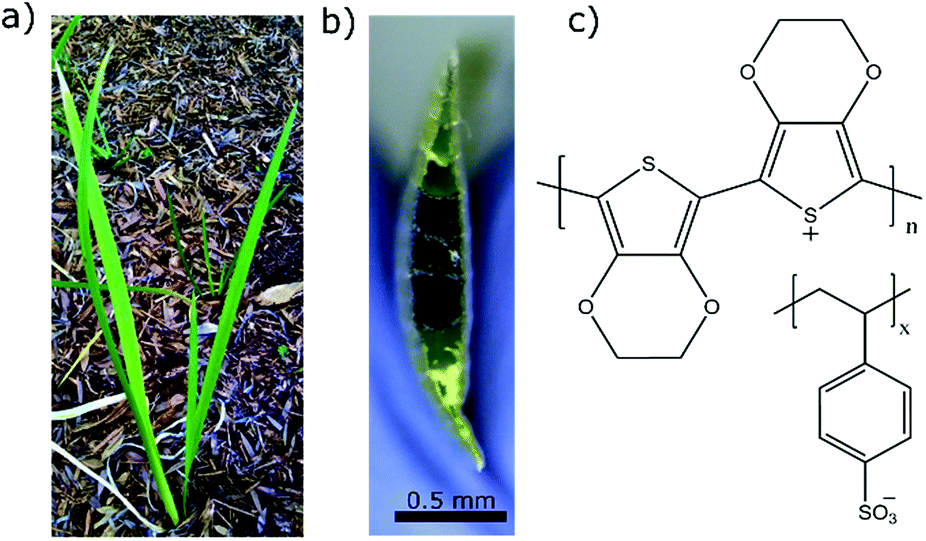 | ||
| Fig. 1 (a) Louisiana iris plant from which the leaf was extracted. (b) Cross sectional image of the leaf with PEDOT:PSS in the conduits which turns the conduits dark in color. The scale bar represents 0.5 mm. (c) Chemical structure of PEDOT:PSS used as conducting polymer to construct conducting wires inside the leaves. | ||
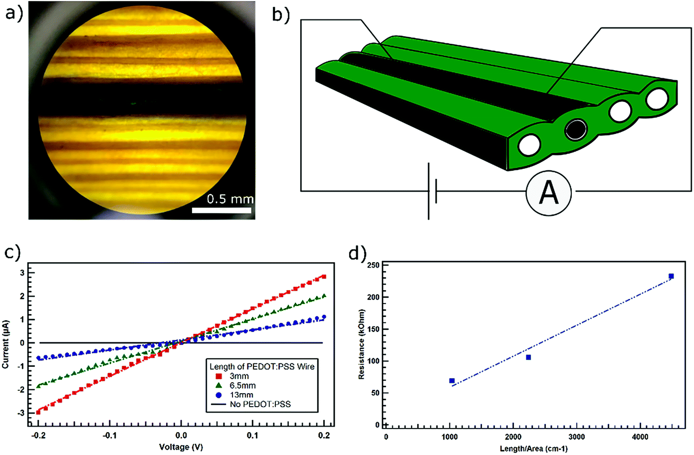 | ||
| Fig. 2 (a) Optical microscope image of channel filled with PEDOT. The PEDOT filled channel is dark thick band. Other channels are lighter in color and are separated by partition wall which can be observed in rest of the leaf image. (b) Sketch of the leaf with PEDOT filled channel and electrical connections for measuring current for applied voltage. (c) Current–voltage (I–V) behaviour of PEDOT conducting channel inside the leaf vesicle in comparison to the response from the vesicle with no PEDOT. The response was ohmic for all the lengths over which the measurement was carried out as shown by the linear fit represented by dotted lines. (d) Resistance of the PEDOT channel as a function of length per area. | ||
2.2 DC measurements
We carried out the measurements under a probe station (Micromanipulator 6200). We made the electrical contacts with 5 μm tungsten probe-tips controlled by micromanipulators (Alessi) which were connected to Keithley 2450 source-measure unit (SMU). We extracted data on the computer by using Keithley's Kickstart software. For current–voltage (I–V) measurements, SMU was used to sweep the voltage and measure the current through the conducting channel in the leaf. For capacitance measurements, the SMU was used for applying voltage or current and Keithley 2110 multimeter was used to measure the voltage across the leaf-based capacitor.2.3 Frequency response measurement
Measurement of capacitance as a function of frequency was carried out using Keysight E4980AL Precision LCR Meter. We measured the capacitance by applying 1 V amplitude within the frequency range of 20 Hz to 300 kHz which is the maximum range available with the equipment.3. Results and discussion
We carried out current–voltage (I–V) measurements in order to investigate the long-range transport through the conducting channel constructed inside the vascular conduit of the leaf (Fig. 2a). A sketch of a typical measurement setup is presented in Fig. 2b. Typical I–V curves generated is presented in Fig. 2c. Intrinsically, the conduits inside the leaves do not conduct. However, when we introduced PEDOT:PSS as the conducting polymer in the conduits, the conducting channels are created. We carried out the measurement for different lengths (3 mm, 6.5 mm & 13 mm) of the conducting channels within a leaf. For all three lengths, we observed the linear response of current to the applied voltage signifying ohmic charge transport along the length of the conducting channels. Using Ohm's law, V = IR, where V is the voltage applied across a conducting channel, I is the current through the channel and R is the resistance of the conducting channel, and applying linear fit, we calculated the resistance of each of the conducting channels. We used the values of the slopes of the linear fit of the I–V-curves, which represent the reciprocal of the resistance, to calculate the resistance of each of the conducting channels. We observed that the resistance of the conducting channels increases with their length (Fig. 2d).Using the cross-sectional image of the conducting channel inside the leaf, we estimated the cross-sectional area to be about 2.9 × 10⁻⁴ cm2. By applying the linear fit to the plot of resistance vs. length per area (Fig. 2d), the contact resistance for this system was found from y-intercept to be about 10 kΩ. Therefore, the true resistance of the PEDOT:PSS filled conducting channel was about 59 kΩ for 3 mm, 95 kΩ for 6.5 mm, and 222 kΩ for 13 mm long wire. We know that the dependence of resistance (R) on length (L) and area (A) can be written as R = L/σA. Using the slope of the linear fit from Fig. 2d, we found the conductivity (σ) of this sample to be about 0.021 S cm−1.
Since the conduits in these leaves are laminar, we decided to investigate if we can construct a capacitor simply by injecting PEDOT on two adjacent vesicles (Fig. 3a). The conduit and partition walls in between the two conducting channels including partition were left to act as a dielectric (Fig. 3b). First, we connected the leaf-based capacitor in series with a 470 kΩ resistor essentially creating an RC circuit. We then measured the current through the circuit as the capacitor charged with a constant voltage of 0.2 V applied by Keithley 2450 SMU. We acquired the current decay curve over time (Fig. 3c) which is typical for current in an RC circuit with a charging capacitor. Using the expression for the current in charging RC circuit (see ESI†), we calculated the time constant to be 12.03 s which gives the value of the capacitance to be about 26 μF. We also carried out measurement of voltage across the capacitor over time while a constant current of 0.2 μA was applied (Fig. 3c) in the circuit by Keithley 2450 SMU. Using the expression for voltage in charging RC circuit (see ESI†), we calculated the time constant to be 12.25 s which also gives the approximate capacitance value of about 26 μF confirming the previous estimate.
 | ||
| Fig. 3 (a) Leaf used for developing a capacitor. Dark lines are conduits filled with PEDOT:PSS. (b) Sketch of setup of leaf used for carrying out capacitance measurements. (c) Current through the capacitor (blue) and voltage across the capacitor (red) as function of time while charging. (d) Voltage across the capacitor (red) as the capacitor charges and discharges while the power is turned on and off (dotted blue). | ||
We also carried out charging and discharging cycles to observe the behavior of the capacitor. We set Keithley 2450 SMU to maintain the potential difference of 0.5 V across the circuit when turned on. We used Keithley 2110 multimeter to record the voltage response across the leaf-based capacitor. As the power applied in the circuit was turned on and off (blue) the capacitor underwent characteristic charging and discharging cycles (Fig. 3d). The maximum voltage during charging and minimum voltage while discharging were set arbitrarily during the first charge–discharge cycle and used as references for upcoming cycles. Subsequent cycles were carried out by charging the capacitor until the capacitor voltage matched the maximum reference voltage from the first cycle. Then, we let the capacitor discharge until the capacitor voltage matched the minimum reference voltage from the first cycle before charging the capacitor again.
We noticed that the discharging time for the leaf-based capacitor is longer than the charging time (Fig. S3, ESI†). The discrepancy in the time for charging and discharging could be due to the mechanism involving the migration of the charges associated with dopants from the conducting polymers into the pores of conduit walls and within polymers. When a bias is applied to charge the capacitor, the dopant induced charge carries could migrate into the pores of the walls of the conducting conduits inside the leaf, and into the grain boundaries of the polymer. When the capacitor discharges, the charges absorbed into the conduit walls or stuck on the grain boundaries would have to be transported along the conducting channels to the contact probes under the influence of weaker and diminishing electric field as the capacitor continues to discharge. Therefore, the discharging process could take longer than the charging process. However, we observe that, over the multiple cycles, both charging and discharging time diminish and start converging. The convergence is possibly due to the dopants filling up the pores on the wall surface and the grain boundaries that can be penetrated through, over the period of multiple cycles. This would make the charge transport along the conducting channel more efficient. The phenomenon of dopants migrating deeper into the plant materials enclosing the conducting channel and within the bulk of the polymer has also been for the system involving doped conducting polymer in xylem conduits of rose stem.13
If we were to quantify the capacitance of such a system, where dopants can move within the polymer bulk and also around the walls of the electrodes, volumetric capacitance would be the relevant parameter to be calculated.13 Using the length of the electrode of about 1.6 cm and cross-sectional area of 29 × 10−5 cm2, we calculated the volumetric capacitance to be about 56 mF cm−3. This value is about the same order of magnitude as the capacitor based on the rose stem.13 This value is also similar to values that have been reported for capacitors based on CNT composites, peptides and conducting polymers.16–18
We then studied the behavior of the leaf-based capacitor in response to the AC voltage applied by an LCR meter. Before carrying out such measurement, one needs to select the simplest circuit model, termed as an equivalent circuit, that best describes the sample under test. We selected the equivalent circuit to be in which a capacitor (Cs) is in series with an equivalent series resistor (Rs) or ESR (Fig. 4a) which is the model used for supercapacitors.19 We observed that the capacitance ranged from 4 μF for 20 Hz to 0.23 nF to 300 kHz (Fig. 4b). It is understandable that the capacitance lowers by orders of magnitude for higher frequency as the polarity changes much faster than the rate with which the electrodes are filled with charges. For the same sample, the equivalent series resistance (ESR or Rs) was found to be varying from 21 kΩ for 20 Hz to 3 kΩ for 300 kHz. While Rs value stays almost within the same order of the magnitude, the value itself is quite high. Rs represents the intrinsic resistance of the capacitor and higher value of it means that the capacitor will dissipate a larger amount of power purely due to internal resistance. For improving the performance, multiple parallel capacitors can be constructed on multiple available conduits within the leaves to maximize the capacitance and minimize the series resistance. Furthermore, it has been reported that the series resistance can be lowered by changing the type of materials used for constructing electrodes or even by introducing electrolyte materials in the dielectrics.20,21 It will be intriguing to see if those techniques can be applied towards the leaf-based capacitors to improve their performance.
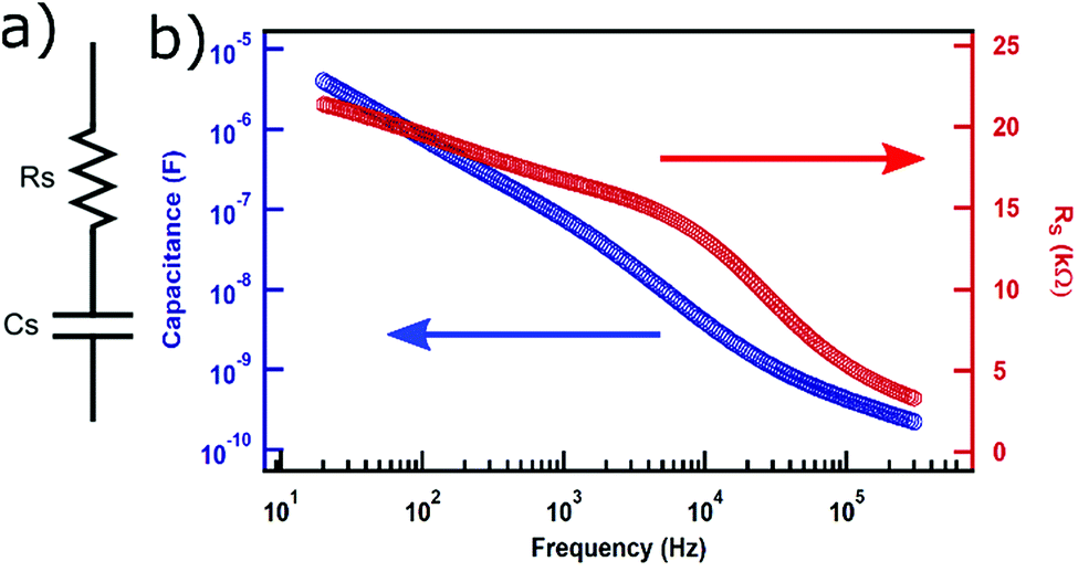 | ||
| Fig. 4 (a) Equivalent circuit used for extracting capacitance (C) and equivalent series resistance (Rs) values from LCR meter. (b) Capacitance (blue) and equivalent series resistance (red) values as function of frequency. | ||
4. Conclusions
We have demonstrated that it is possible to create conducting pathways within the vascular conduits inside leaves and construct electronic devices based on the architecture of those conduits. By using elongated conduits on the leaves of a monocotyledon plant, we were able to develop centimeter length-scale conducting wires within leaves. Taking advantage of the laminar conduits, we were able to construct parallel electrodes to fabricate supercapacitors within the leaves. While there is a need for further research in improving the performance of such capacitors, it is certainly exciting that electronic components can be developed within plant parts. As the interest in biodegradable, biocompatible and flexible electronics continues to grow, these developments should help realize the potential of using plant materials and taking advantage of the architectures of their vascular conduits to develop sustainable electronics. Furthermore, findings and methods presented here may be useful in the research involving study of plant behaviors using their electrical signals.Conflicts of interest
There are no conflicts to declare.Acknowledgements
We like to thank Misha Chalkley, Festus Ogbaisi, Brian Stadelmaier and Carla Garcia for their technical support. This research was supported by The Eppley Foundation for Research and Collaborate JU which is a part of Florida EPIC (Entrepreneurism, Policy, Innovation, and Commerce) program at Jacksonville University.Notes and references
- H. Kharas, The unprecedented expansion of the global middle class, https://www.brookings.edu/research/the-unprecedented-expansion-of-the-global-middle-class-2/, accessed 2 June 2019.
- Bureau of Labor Statistics, Long-term price trends for computers, TVs, and related items: The Economics Daily: U.S. Bureau of Labor Statistics, https://www.bls.gov/opub/ted/2015/long-term-price-trends-for-computers-tvs-and-related-items.htm, accessed 4 June 2019.
- S. F. Ahmed, E-waste: The Global Cost of Discarded Electronics - The Atlantic, https://www.theatlantic.com/technology/archive/2016/09/the-global-cost-of-electronic-waste/502019/, accessed 4 June 2019.
- United Nations, Electronic waste poses ‘growing risk’ to environment, human health, UN report warns|UN News, https://news.un.org/en/story/2017/12/639312-electronic-waste-poses-growing-risk-environment-human-health-un-report-warns, accessed 4 June 2019.
- D. T. Simon, E. O. Gabrielsson, K. Tybrandt and M. Berggren, Chem. Rev., 2016, 116, 13009–13041 CrossRef CAS PubMed.
- H. Zhu, W. Luo, P. N. Ciesielski, Z. Fang, J. Y. Zhu, G. Henriksson, M. E. Himmel and L. Hu, Chem. Rev., 2016, 116, 9305–9374 CrossRef CAS PubMed.
- G. Zan and Q. Wu, Adv. Mater., 2016, 28, 2099–2147 CrossRef CAS PubMed.
- M. J. Tan, C. Owh, P. L. Chee, A. K. K. Kyaw, D. Kai and X. J. Loh, J. Mater. Chem. C, 2016, 4, 5531–5558 RSC.
- M. Irimia-Vladu, E. D. Głowacki, G. Voss, S. Bauer and N. S. Sariciftci, Mater. Today, 2012, 15, 340–346 CrossRef CAS.
- J. G. H. Whiting, R. Mayne, N. Moody, B. de Lacy Costello and A. Adamatzky, Biomedical Engineering Letters, 2016, 6, 57–65 CrossRef.
- A. Adamatzky, Biosystems, 2014, 122, 1–6 CrossRef PubMed.
- E. Stavrinidou, R. Gabrielsson, E. Gomez, X. Crispin, O. Nilsson, D. T. Simon and M. Berggren, Sci. Adv., 2015, 1, e1501136 CrossRef PubMed.
- E. Stavrinidou, R. Gabrielsson, K. P. Nilsson, S. K. Singh, J. F. Franco-Gonzalez, A. V. Volkov, M. P. Jonsson, A. Grimoldi, M. Elgland, I. V. Zozoulenko, D. T. Simon and M. Berggren, Proc. Natl. Acad. Sci. U. S. A., 2017, 114, 2807–2812 CrossRef CAS PubMed.
- D. Tobjörk and R. Österbacka, Adv. Mater., 2011, 23, 1935–1961 CrossRef PubMed.
- A. Russo, B. Y. Ahn, J. J. Adams, E. B. Duoss, J. T. Bernhard and J. A. Lewis, Adv. Mater., 2011, 23, 3426–3430 CrossRef CAS PubMed.
- K. Hu, C. Zheng, M. An, X. Ma and L. Wang, J. Mater. Chem. A, 2018, 6, 8047–8052 RSC.
- Poonam, K. Sharma, A. Arora and S. K. Tripathi, J. Energy Storage, 2019, 21, 801–825 CrossRef.
- G. A. Snook, P. Kao and A. S. Best, J. Power Sources, 2011, 196, 1–12 CrossRef CAS.
- Maxwell Technologies, Application Note: Test procedures for capacitance, 2015 Search PubMed.
- P. Milani, L. Diederich, E. Barborini, P. Piseri, A. Podesta, A. Schneuwly and R. Gallay, Appl. Phys. Lett., 1999, 75, 2662–2664 CrossRef.
- Y. Show and K. Imaizumi, Diamond Relat. Mater., 2006, 15, 2086–2089 CrossRef CAS.
Footnote |
| † Electronic supplementary information (ESI) available. See DOI: 10.1039/c9ra05287a |
| This journal is © The Royal Society of Chemistry 2019 |