
 Open Access Article
 This Open Access Article is licensed under a Creative Commons Attribution-Non Commercial 3.0 Unported Licence
Electrodeposition of nanowires of a high copper content thiourea precursor of copper sulfide†
Abhisakh
Sarma
 *a,
Ann-Christin
Dippel
a,
Olof
Gutowski
a,
Martin
Etter
a,
Milena
Lippmann
a,
Oliver
Seeck
a,
Gouranga
Manna
b,
Milan K.
Sanyal
b,
Thomas F.
Keller
ac,
Satishkumar
Kulkarni
a,
Puspendu
Guha
d,
Parlapali V.
Satyam
d and
Martin V.
Zimmermann
a
*a,
Ann-Christin
Dippel
a,
Olof
Gutowski
a,
Martin
Etter
a,
Milena
Lippmann
a,
Oliver
Seeck
a,
Gouranga
Manna
b,
Milan K.
Sanyal
b,
Thomas F.
Keller
ac,
Satishkumar
Kulkarni
a,
Puspendu
Guha
d,
Parlapali V.
Satyam
d and
Martin V.
Zimmermann
a
aDeutsches Elektronen-Synchrotron DESY, Notkestraβe. 85, 22603 Hamburg, Germany. E-mail: abhisakh@gmail.com
bSurface Physics and Materials Science Division, Saha Institute of Nuclear Physics, 1/AF, BidhanNagar, Calcutta 700 064, India
cPhysics Department, Universität Hamburg, Jungiusstraße 9, 20355 Hamburg, Germany
dInstitute of Physics, Sachivalaya Marg, Bhubaneswar 751005, Odisha, India
First published on 7th October 2019
Abstract
Copper thiourea complexes are an important material class for application as a precursor of copper sulfide nanocrystals with potential use in solar cells, optoelectronics, medicine, etc. They represent a type of single source precursor, comprising both copper and sulfur in one chemical compound, whose tunable stoichiometry and morphology enable control of the quality and properties of the synthesized copper sulfide nanocrystals. Here, we present a template free electrochemical route to prepare nanowires of copper thiourea (tu) chloride hemihydrate ([Cu(tu)]Cl·½H2O) by pulse deposition. We proposed the model of the growth of nanowires. We also demonstrate complete transformation from the precursor to copper sulfide nanowire by heating it to 180 °C that involves 20% volume loss due to the decomposition of organic constituents; the obtained nanowires have around 38% covellite (CuS) and 62% digenite (Cu1.8S) phases. Electrochemistry offers the advantage of spatially selected deposition e.g. in the active regions of a device.
Introduction
Metal sulfide nanomaterials have attracted attention in the last two decades owing to their novel optical and electronic properties that emerge due to quantum confinement.1–3 Toxicity of most of the metal chalcogenides limits their possible applications. However, the abundance and relatively low toxicity of copper sulfide make it a promising candidate for diverse applications in numerous fields including energy harvesting and storage,4–8 photocatalysis,9,10 optoelectronics,11–14 sensors, as well as in microbiology,15 and medical diagnostics16–18 and therapy.19–21 Various stoichiometries, phases, and morphologies of copper sulfide nanomaterials and their related functional properties have been studied.22–26 For the fabrication of copper sulfide nanoparticles with varying, tailor-made morphologies,22,26,27 different synthesis techniques have been used.24,25,28,29 Among these, synthetic routes based on dry single source precursors for copper and sulfur are of particular interest because they are cost effective, employ relatively low temperatures (80 to 200 °C), and produce high quality uniform nanocrystals.30–34 Hence, this low temperature synthesis of copper sulfide from single-source precursors is particularly relevant e.g. during its incorporation and layer processing in flexible thin film solar cells.30–33 Some studies have shown that the morphology of the resulting nanoparticles and their stoichiometry can be tuned not only by changing precursor concentration,35 reaction time,36 temperature37 and anions,38 but also by varying the morphology of the precursor material.39 Jun et al. reported that nanowire or nanocone shaped precursors can be utilized as a sacrificial template to synthesize hierarchical structures of copper sulfide in different shapes and sizes.39Copper thiourea complexes (CTCs) are well-known single source precursors for copper sulfide nanocrystals. CTCs are chelate complexes of the form [Cu(tu)n]Xy, with tu as a symbol for the thiourea ligand H2N–CS–NH2 and X representing coordinated anions such as Cl−, SO42− as well as water molecules. In the last 50 years, various CTCs have been reported.25,26,38,40–43 Despite the advantages of the single source precursor technique mentioned above, a major drawback is the evolution of organic byproducts during pyrolysis. The presence of these byproducts may interfere with the function of the copper sulfide device, e.g. it strongly affects the quantum efficiency of CuS based solar cells.44 Hence, the minimization of organic residues is essential to optimize the device performance. To this end, Krunks et al.43 compared the decomposition of the CTCs copper thiourea chloride hemihydrate [Cu(tu)]Cl·½H2O and copper tris thiourea chloride hydrate [Cu(tu)3]·Cl·H2O. They showed that the precursor with lower thiourea content, i.e. 1 tu ligand per formula unit as opposed to 3, produces less unwanted C–H–N-containing polymeric resin.43,45 In our work, we thus focus on this CTC [Cu(tu)]Cl·½H2O with low thiourea content.
Krunks et al.46 and Han et al.47 reported the chemical synthesis of polycrystalline thin films and very high aspect ratio nanowires of [Cu(tu)]Cl·½H2O, respectively. In addition, thin films of various CTCs, such as [Cu2(tu)5]SO4·3H2O, [Cu4(tu)7(SO4)2]·3H2O, [Cu2(tu)6]SO4·H2O48–51 have been prepared by electrochemical deposition. However, an electrochemical route for nanowires of the particular CTC [Cu(tu)]Cl·½H2O has, to our knowledge, not yet been reported. The unique advantage of electrodeposition over other techniques is the spatial selectivity, i.e. electrodeposition only occurs at those locations of the conducting electrode which are in contact with the electrolyte.52 Consequently, electrodeposition is especially useful for the nanofabrication of functional materials inside electronic chips.52
In general, an electrolyte for the electrodeposition of CTCs consists of a copper salt (e.g. CuSO4), thiourea, and an acid such as HCl or H2SO4.48–51 The reaction and growth mechanisms of electrochemically derived CTCs were studied by several groups. Bolzán and Haseeb reported that the morphology (smooth film to discrete islands) and stoichiometry (copper(I), copper(II), or mixed oxidation state copper thiourea complexes) of the CTC product strongly depends on the ratio of molar concentrations of thiourea and copper in the electrolyte, as well as on the applied voltage.48–51 A solution having a thiourea concentration at least four times higher than the concentration of copper ions provided a chemical equilibrium to form only monovalent copper thiourea complex cations [Cu(tu)]+.48 The application of DC voltage in the range of −0.7 to −0.8 V in such a solution readily reduces the copper ions so that they deposit as metal on the working electrode.53–55 In a potentiometric study, it was shown that at zero voltage applied to the working electrode, thiourea adsorbs on the deposited copper. At the same time copper starts to dissolve into the solution, re-complexes with the adsorbed thiourea, and reacts with the anion of the acid (e.g. Cl−, SO42) to form an insoluble film at the copper surface.56 The formed CTC is quite stable, and its dissolution requires the application of positive voltage of 0.075 V.49–51,57,58 At higher voltages, the electrodecomposition of the complex yields heterogeneous products of non-stoichiometric copper sulfide and copper cyanide species.49–51,57,58 Ghahremaninezhad et al.,23 however, reported that copper sulfide nanowires form already at lower voltages (V ≤ 0) when applying repeated pulses of negative and zero voltage (−0.85 V ≤ V ≤ 0) in a solution of copper sulfate, thiourea and hydrochloric acid.
In this work, we employed an electrochemical synthesis route comparable to that introduced by Ghahremaninezhad et al.23 and found that the reaction product are nanowires predominantly composed of the CTC [Cu(tu)]Cl·½H2O without any traceable amount of copper sulfide. As a first and obvious indicator, the obtained product was white instead of dark color such as blue, black, or green which are typical for copper sulfide of different stoichiometries. The identification of the synthesized material as [Cu(tu)]Cl·½H2O and its discrimination from copper sulfide is based on a combination of several analysis techniques that probe the chemical and structural nature of the material. For this purpose, we carried out energy-dispersive X-ray spectroscopy to derive the elemental composition incl. light elements, X-ray diffraction for information on the crystal structure, as well as infrared and Raman spectroscopy to identify the existing bonds and functional groups. Due to the structural similarity of CTCs and copper sulfide, we were only able to unambiguously distinguish between the two compounds by confirming the presence of the light elements carbon and nitrogen plus chloride, as well as by the evidence for the functional amino and thioketone groups. Electron microscopy was applied to study the morphology and grain structure of the nanowires. These results were complemented by analyzing the optical absorption spectra of the CTCs with respect to the bandgap. In this way, we determined that the CTC exhibits a direct bandgap suitable for classification as a wide bandgap material, as well as an indirect bandgap. At 180 °C, the transformation of the nanowires from CTC into copper sulfide was achieved. The resulting nanowires were analyzed with respect to morphology, crystal and chemical structure.
Experimental section
Electrochemical synthesis
We electrochemically synthesized CTC nanowires in a three electrode configuration, as shown in Fig. 1. A 0.25 mm thick platinum foil with 99.9% purity (Alfa Aesar) served as working electrode, a graphite foil (Alfa Aesar) of 1 mm thickness as counter electrode, and a standard Ag/AgCl electrode as reference electrode. The edges of the foils were insulated by a layer of varnish to avoid local peak fields at the electrodes. The area of the counter electrode was five times larger than the working electrode to avoid the current limit in the cell due to the reaction at the counter electrode (e.g. hydrogen evolution). We applied rectangular pulse trains as described below, generated by a HP 8116A 50 MHz pulse function generator. A standard potentiostat circuit was used that consisted of an integrator combined with a Tektronix MDO3000 mixed domain oscilloscope to maintain and monitor voltage, current, and frequency in the electrochemical cell. The potential of the working electrode was kept stable relative to the reference electrode. In order to avoid current drawing through the reference electrode, we used a buffer circuit. Before and after each reaction, the working electrode was rinsed using a 3![[thin space (1/6-em)]](https://www.rsc.org/images/entities/char_2009.gif) :1 mixture of HCl and HNO3 for 2 min and subsequently washed using deionized water. For each synthesis run, a fresh graphite electrode was inserted.
:1 mixture of HCl and HNO3 for 2 min and subsequently washed using deionized water. For each synthesis run, a fresh graphite electrode was inserted.
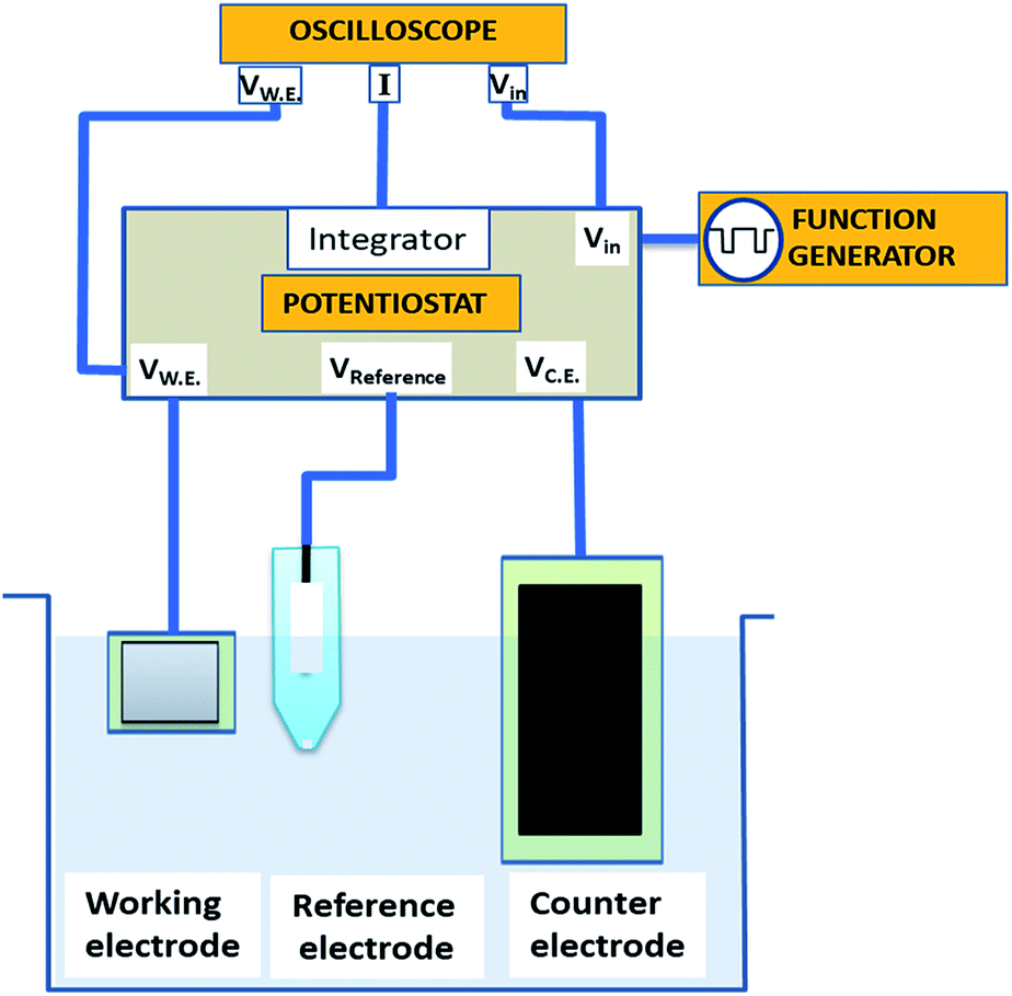 | ||
| Fig. 1 Schematics of pulse deposition in a three electrode configuration. Here VW.E., VReference and VC.E. represent the potential of working, reference and counter electrode respectively. | ||
During the electrodeposition, we applied 33 Hz rectangular pulse trains with the upper and lower voltage limits being VR = 0 V and VF = −0.85 V, respectively (see Fig. 2a). Here, the subscripts ‘R’ and ‘F’ denote ‘reverse’ and ‘forward’ potential of the working electrode, respectively. The measured potential between the working electrode and the standard electrode is shown in Fig. 2b. The anodic current during application of VR and the cathodic current during the application of VF are shown in Fig. 2c. In each cycle, VR was applied for 24 ms and VF for 6 ms, i.e. 20% of the duty cycle. The entire deposition time was 1 h.
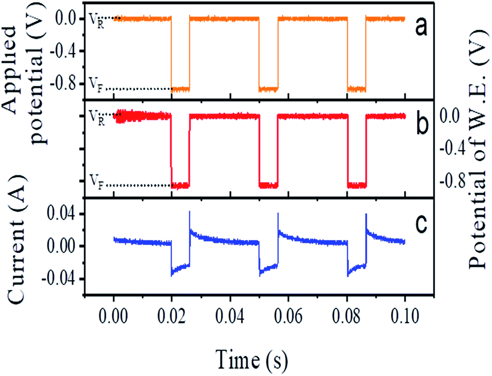 | ||
| Fig. 2 Plot of (a) applied potential and (b) recorded potential at the working electrode (W.E.) with respect to the reference electrode, (c) measured current, during synthesis. | ||
The electrolyte consisted of 1 mmol per L per CuSO4, 5H2O and 4 mmol per L per thiourea (tu) as the sources of copper and sulfur, respectively. 149.2 mg of CuSO4·5H2O were dissolved in 300 mL of water, yielding a concentration of 2 mmol L−1. 5 mL of concentrated hydrochloric acid were mixed into this copper sulfate solution. An 8 mmol per L per tu solution was prepared by dissolving 177.4 mg per tu in 300 mL water. Both solutions were mixed and stirred for 30 min. The final electrolyte had a pH of 1.2.
For the annealing study, a nanowire ensemble was placed on a silicon nitride hot plate (Bach Resistor Ceramics) at 5 °C min−1 in air to the final temperature of 180 °C.
Analysis
The morphology of the synthesized nanowires was studied using a high-resolution field-emission electron microscope (SEM) model Nova Nano SEM 450 (FEI)59 on samples dispersed on silicon substrates. In case of the single nanowire that was subjected to thermal treatment, a platinum marker was deposited by a dual-beam focused ion beam (FIB) instrument SCIOS (FEI).59 Elemental analysis of the SEM samples was performed by energy dispersive X-ray spectroscopy (EDS) using an X-Max 150 silicon drift detector with a 150 mm2 large active area (Oxford Instruments).59 A JEOL JEM-2010 high resolution transmission electron microscope (HRTEM) was used to investigate the morphology and structure. In order to study the morphology inside the nanowires at high resolution, we prepared the cross section from a nanowire along its long direction using FIB and mounted it on a FIB lift out TEM grid from micro to nano.The X-ray diffraction (XRD) measurements were performed using photon energy of 80 keV at beamline P07, PETRA III, DESY (Hamburg, Germany). The powder diffraction data were collected on a PerkinElmer XRD1621 area detector in the q range from 0.3 to 3.8 Å−1 with a resolution of 0.004 Å−1. The beam size was 50 × 100 μm2. In order to characterize the functional groups, we performed Fourier transform infrared spectroscopy (FTIR) using a HYPERION optical microscope spectrometer. The signal was collected using a 15× IR objective in combination with a focal plane array (FPA) detector. Raman spectra were recorded using a SENTERRA spectrometer with a microscope setup at an excitation wavelength of 532 nm. The spectra were collected at a resolution of 9 cm−1 with 50 μm diameter aperture in front of the CCD camera. Absorption spectra in the ultraviolet and visible range from 300 to 1100 nm were recorded using a dual channel AVASPEC-ULS2048L spectrometer (Avantes). The diffuse reflected signal was collected with an FCR-7UVIR400-2-BX reflection probe. The white standard WS-2 (Avantes) which is made out of a white diffuse PTFE based material was used for reflectance calibration in the applied wavelength range.
SEM, EDS, FTIR, Raman and optical absorption spectroscopy were performed on ensembles of nanowires collected on a 1 × 1 cm2 silicon wafer after exfoliating them from the working electrode. Likewise, we transferred the nanowires to a 200 μm thick glass microscope cover slip for the X-ray diffraction measurement.
Cyclic voltammetry (CV) was performed on the described electrolyte as well as a corresponding solution without thiourea using the same potentiostat as for the synthesis and a Keithley 4200 SCS to detect the current. Staircase CV measurements were performed in the voltage range 0 to −1 V at a step size of 0.002 V and a step period of 0.1 s. High frequency current measurements were carried out by applying voltage pulses using the function generator and recording the current response with the oscilloscope. The forward voltage VF and the frequency were varied in the range −1 to −0.3 V and 5 to 500 Hz, respectively.
Results and discussion
Morphology and composition
A representative SEM micrograph of electrochemically synthesized nanowires is presented in Fig. 3b. As can be seen, the aspect ratio of the nanowires is very high, with the diameter ranging between 80 nm and 350 nm and the length in around 100 μm. Apart from the Si signal from the substrate the EDS spectrum presented in Fig. 3a confirms the presence of copper, sulfur, chlorine, nitrogen, carbon, and oxygen. In addition, the elemental mappings of the nanowire depicted in Fig. 3d–i show the uniformity of those elements along the length of the nanowire. Overall, these EDS results qualitatively identify the constituents of the sample and the mappings illustrate their spatial distribution. However, the elemental stoichiometry of a composite material consisting of light, like, e.g., C, N, O and heavier elements like Cu cannot be easily quantified with the required precision for non-flat surfaces like in the case of the here analyzed nanowires. The major systematic error in the composition calculation based on EDS originates from the electron-density and therefore element-dependent penetration depth and excitation volume,60 which itself depends on the nanowire shape.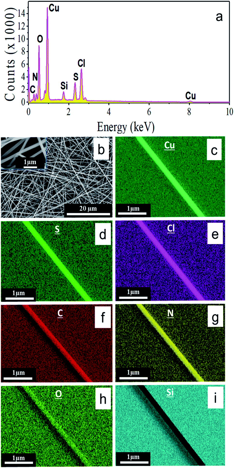 | ||
| Fig. 3 (a) Energy dispersive X-ray spectra of nanowires drop-casted on a silicon substrate, indicating the presence of Cu, S, Cl, C, N, O, and Si; (b) representative SEM micrograph of the synthesized nanowires with diameters in the range of 80–350 nm and a length of ∼100 μm. The inset shows a magnified region with nanowire segments. (c–i) Elemental maps of one nanowire segment, illustrating that the origin of Cu, S, Cl, C, N, O is the nanowire and the source of the Si signal is the substrate, respectively. (c–i) Indicate the uniformity of the elemental distribution along nanowire. | ||
Crystallinity and structure
To identify the material and in particular its crystallinity we performed high resolution transmission electron microscopy (HRTEM). Since the full nanowire thickness of around 350 nm cannot be penetrated by HRTEM, we prepared a nanowire cross-section by FIB. The Ga ion beam was thereby used to create in a first step a lamellar sample of the silicon with the nanowire on top that was subsequently thinned down along the length of the nanowire axis. Fig. 4a and b depicts the initial and final stage of the FIB based cross-section preparation, respectively. The parallel green lines in Fig. 4b indicate the final lamellar thickness of 30 nm.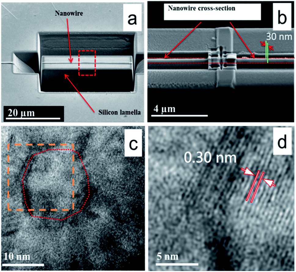 | ||
| Fig. 4 (a) Low magnification SEM image of a single nanowire on top of a silicon lamella created by FIB based cross-section preparation and subsequent lamella thinning. (b) Magnified SEM image of the portion marked as red dashed box in (a). The zone between two parallel red dotted lines represents the width of the nanowire after thinning down to a cross-section thickness of 30 nm (green lines). (c) HRTEM image of the prepared cross-section showing a single grain of around 18 nm diameter as marked by the red dotted line. (d) Digitally magnified picture of the zone marked by the orange dotted box in (c) from which a lattice constant of 0.3 nm was determined. This value matches well with the predicted (112) plane of the CTC (ref. 61) as well as Cu1.94S (ref. 63) and Cu2S planes (ref. 62). | ||
The obtained TEM images shown in Fig. 4c and d revealed that the nanowire was polycrystalline in nature with crystallite sizes in the range of 15 to 30 nm. Fig. 4c shows a representative micrograph from the exploration of different regions of the cross-section. For visualization of crystal planes, a digitally magnified image of the portion marked by the orange dashed box in Fig. 4c is presented in Fig. 4d. The lattice spacing calculated from the HRTEM image is 3.0 Å, which matches well with the distances of the (112) planes of the CTC [Cu(tu)]Cl·½H2O61 as well as copper-sulfur phases such as Cu2S62 and Cu1.94S.63 The combination of the presence of this lattice spacing with the elemental information from EDS, however, points towards the sample being the CTC rather than a copper sulfide derivative. None of the TEM images collected along the length of the cross section over several tens of micrometers revealed any detectable traces of unreacted copper.
In Fig. 5, room temperature diffraction data of the nanowires are presented along with reference data for the CTC [Cu(tu)]Cl·½H2O.61 The two-dimensional diffraction pattern in the inset shows continuous Debye–Scherrer rings with a constant azimuthal intensity distribution. Hence, it reveals that the sample, consisting of an ensemble of the polycrystalline nanowires as confirmed by TEM, is randomly orientated. While the upper panel of Fig. 5 shows that most peak positions and intensities match well, the zoom into the low intensity region shown in the lower part of Fig. 5 demonstrates that the diffraction pattern of the sample contains a few additional reflections (indicated by the black arrows) that are not present in the reference pattern. These extra reflections might originate from a secondary phase of the CTC, but it cannot be ruled out that they stem from the same structure for which only incomplete structural information is available.61 In ref. 61, the probable unit cell was proposed as monoclinic without defining the space group. The measured reference pattern64 given in ref. 64, contains unassigned reflections as well. Since the diffraction data presented in this work was recorded at higher angular resolution and higher signal to noise ratio, additional unidentified reflections are present besides the previously reported unassigned peaks from ref. 64. On this basis, a detailed structure determination of the sample including phase analysis and description of preferred orientation is not possible.
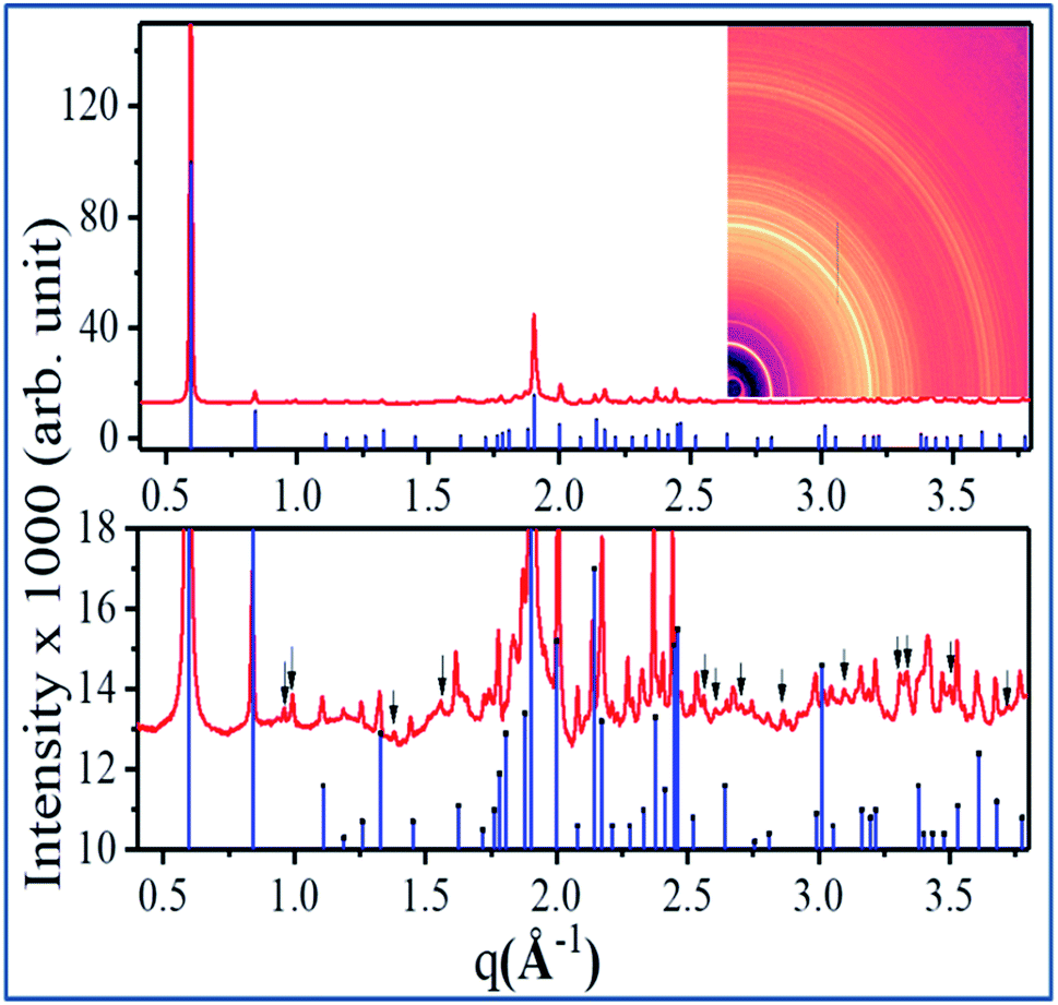 | ||
| Fig. 5 Comparison of a typical X-ray diffraction pattern obtained from the synthesized nanowires (red) along with the reference structure of Cu(tu)Cl·½H2O (ICDD PDF 00-053-0121, (blue) in the q range 0.4–3.8 Å−1). The upper panel shows full intensity range, the lower panel is a magnification of the low intensity region in which a few reflections are marked by black arrows which are not described by the reference. The inset shows the corresponding two-dimensional diffraction pattern in the same q range. | ||
Chemical structure
FTIR and Raman absorption spectra of the nanowire sample are shown in Fig. 6a and b. We used reference data for ([Cu(tu)]Cl·½H2O) which was published by Krunks et. al.46 to assign the absorption bands of the FTIR spectrum as listed in Table 1.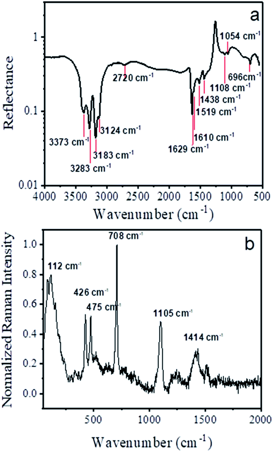 | ||
| Fig. 6 (a) FTIR and (b) Raman spectra collected from ensembles of nanowires in reflection mode with marked wavenumbers of the minima and maxima, respectively. | ||
| FTIR bands (cm−1) | Literature values46 | Assigned modes |
|---|---|---|
| 3373 | 3371 | ν(OH), ν(NH), [ν(OH)] |
| 3283, 3183, 3124 | 3279, 3177, 3122 | ν(OH), ν(NH) |
| 2720 | 2718 | Not yet assigned |
| 1629 | 1621 | δ(NH2), [δ(OH2)] |
| 1519 | 1515 | Not yet assigned |
| 1438 | 1415 |
ν(N–C–N), δ(NH2)+, ν(N–C–N)+, ν(C![[double bond, length as m-dash]](https://www.rsc.org/images/entities/char_e001.gif) S) S) |
| 1108 | 1107 |
ν(N–C–N)+, δ(NH2)+, ν(CS) |
| 1054 | 1055 | Not yet assigned |
| 696 | 696 |
ν(CS)+, ν(N–C–N) |
The remaining three bands visible in the spectrum at around 2720 cm−1, 1519 cm−1 and 1054 cm−1 were also detected by several groups for the same CTC composition [Cu(tu)]Cl·½H2O,46,47,65 yet they have not been assigned to any particular modes. In a similar way, the Raman shift data was interpreted according to ref. 66 as tabulated in Table 2. Overall, there is a very good agreement of our obtained FTIR and Raman spectra with the reported data for the CTC ([Cu(tu)]Cl·½H2O).
| Observed Raman bands (cm−1) | Literature values66 | Assigned modes |
|---|---|---|
| 1414 | 1420 |
ν(C–N), ν(CS), ρ(H–N–H) |
| 1105 | 1101 | ν(C–N), ρ(H–N–H) |
| 708 | 732 |
ν(CS) |
| 426, 475 | 428, 476 | δ(N–C–N), δ(S–C–N) |
| 112 | 118 | Presence of Cl− |
For copper sulfide, both FTIR and Raman spectra show only few bands connected bonds between copper and sulfur on the one hand and between sulfur atoms on the other hand.
Our spectra show bands at similar positions (1103 cm−1 in FTIR, 470 cm−1 in Raman67), but in addition many more bands of the H2N–CS–NH2 group of the thiourea ligand.
Optical properties and bandgap
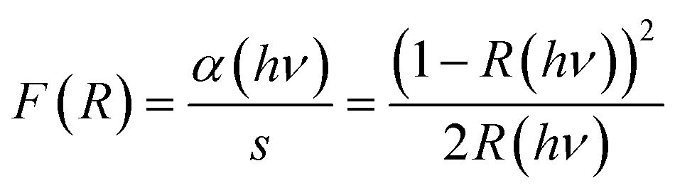
The diffuse reflectance spectrum of the sample is presented in Fig. 7a. We used the Kubelka–Munk theory for the calculation of the absorption coefficient α(hν) from the obtained reflectance spectrum according to the formula68here F(R) is the Kubelka–Munk function, R the reflectance, α the absorption coefficient and s the scattering factor. F(R) is proportional to α as s is independent of the photon energy hν. The relationship between F(R) and the energy of the incident photon in the vicinity of the absorption edge can be described by the modified Tauc equation,68,69
| F(R)hν = A(hν − Eg)1/n |
 | ||
| Fig. 7 (a) Diffuse reflectance spectrum of the sample, (b) modified Tauc plot for the exponent value of n = 1/2 (left y-axis, indirect transition) and n = 2 (right y-axis, direct transition), here F(R) is the Kubelka–Munk function. | ||
Electrochemical reaction mechanism
In electrochemical syntheses, numerous parameters such as voltage, frequency, as well as electrolyte composition and concentration determine what processes take place at the working electrode. The cyclic voltammogram depicted in Fig. 8a describes the current response to the application of a working electrode potential in the range of −0.85 to 0 V in our electrochemical cell.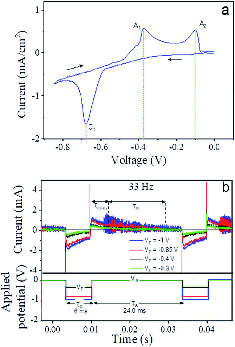 | ||
| Fig. 8 (a) Cyclic voltammogram obtained from an 0.1 M HCl solution containing copper sulfate and thiourea, (b) current pulses (upper section) recorded during the synthesis of CTC nanowires using 33 Hz rectangular voltage pulses of four different amplitudes between −1 and −0.3 V as illustrated in the lower section. | ||
Three distinct peaks were detected, one during the sweep towards negative voltage (peak cathodic current, C1) at −0.68 V and two during the reverse part of the cycle (peak anodic currents, A1 and A2) at −0.37 V and −0.01 V. According to the ref. 23 and 75, the cathodic current is indicative of the deposition of metallic copper on the working electrode from an acidic solution of copper sulfate and thiourea of the given concentration. For comparison, when the electrolyte did not contain any thiourea that binded the copper in ligand form, copper deposited from its solvated ionic state in the solution at a higher working electrode potential of −0.24 V (compare Fig. S1a in the ESI†). During the reverse sweep, the deposited copper is dissolved in two distinct processes as specified in ref. 23, i.e. the reaction of copper with thiourea at −0.37 V and the reaction of copper with chloride ions from the solution at −0.01 V. When applying a smaller voltage range of 0 to −0.45 V, the corresponding CV curve shows a flat baseline (see inset of Fig. S1b, in the ESI†) and, hence, demonstrated that neither deposition nor dissolution of copper took place. From these results, it was clear that a forward potential <−0.68 V had to be chosen to induce the deposition of copper as the initial step of the nanowire growth as discussed in detail below.
In contrast to the stepwise application of static potentials in the cyclic voltammetry measurements, the nanowire synthesis was carried out in pulsed mode with a frequency of 33 Hz. This means that one duty cycle, i.e. the application of VF for copper deposition and VR for copper dissolution, takes 30 ms (see Fig. 8b). Highly time-resolved current measurements that were performed at the chosen pulse frequency and varying VF (see Fig. 8b) illustrate the time structure of the two step process (V = VF deposition, V = VA reaction). Appearance of the visible initial sharp spikes only during the change of the voltage state (VF to VA or vice versa) which is due to the double layer capacitance formed at electrode electrolyte interface. After the change of the pulse state the recovery process of local ion concentration takes place and the current approaches to a steady state with time. In agreement with the CV results, the comparison of the recorded cathodic current over the entire application period of VF for VF ≤ −0.85 V with that VF ≥ −0.4 V reveals that the cathodic current is significantly smaller and relaxes to almost zero over the course of the negative phase of the pulse for pulses with VF ≥ −0.4 V. After returning back to VR = 0 V, there is practically no response observable for VF ≥ −0.4 V. This is comprehensible in the sense that there can be no dissolution and reaction without prior deposition. In the case of the lower VF (much negative) values, on the other hand, we observed a fluctuating anodic current with decreasing amplitude that approached zero at the end of the duty cycle. These fluctuations set in after a certain delay time in the range of 3–4 ms. It was reported56 that the dissolution of copper in the presence of thiourea in the solution is slow,74 and the current fluctuations suggested that it occurred discontinuously. As the anodic current was close to zero before switching back to the forward potential in case of VF = −0.85 V, it can be assumed that the dissolution/reaction of the metallic copper was nearly complete. But in case of VF = −1 V the fluctuations remains before switching back to the forward potential. At shorter pulse lengths, the available time at VR is shorter and, above a certain frequency, insufficient to complete the copper dissolution. Longer pulse durations do not essentially provide any benefit as they lead to longer idle time after completing the dissolution and before starting the next deposition. The time structures for selected frequencies between 5 and 500 Hz with a fixed duty cycle proportion of 20% of the entire pulse length at potential VF and 80% at VR are given in Fig. S2 in the ESI.† These results elucidate that the parameters chosen here for the electrodeposition, i.e. 33 Hz pulse frequency and VF = −0.85 V provide for efficient growth conditions for the CTC nanowires.
As mentioned in the introductory section, a detailed description of different reaction pathways for the electro-chemical synthesis of copper sulfide nanowires under various reaction conditions is found in a report by Ghahremaninezhad.23 When transferring the proposed model to our route and considering our findings as described above, we divide the CTC nanowire synthesis into three stages: (i) the redox reaction and complexation upon mixing of the copper sulfate and thiourea solutions to prepare the electrolyte, (ii) the deposition of metallic copper at the working electrode during the application of VF = −0.85 V, and (iii) the nanowire nucleation and growth at VR = 0 V. Steps (ii) and (iii) of the CTC nanowire growth are schematically illustrated in Fig. 9.
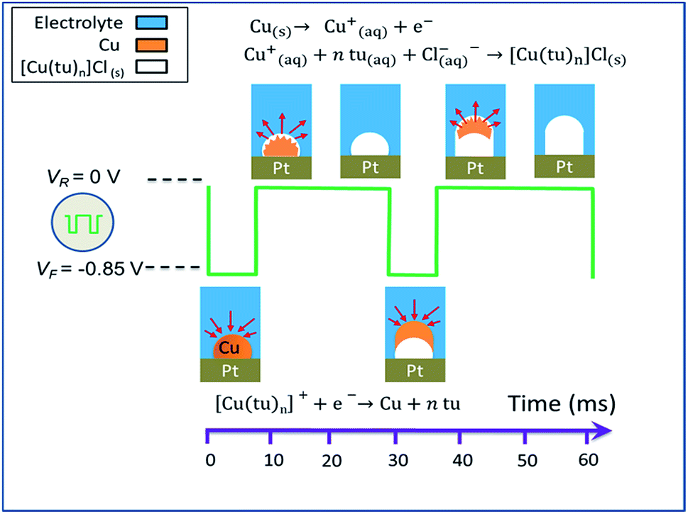 | ||
| Fig. 9 Schematic illustration of the pulse electrodeposition of [Cu(tu)]Cl·½H2O nanowires (crystal water not included in the reaction equations). | ||
(i) When the copper sulfate and thiourea solutions are mixed, a redox reaction between the cupric ions Cu2+ and thiourea takes place according to
| 2Cu2+ + 2tu ↔ 2Cu+ + FDS + 2H+ | (1) |
| Cu+ + ntu ↔ [Cu(tu)n]+ | (2) |
It was shown for a dominant thiourea molar concentration that the primarily formed complex cations are Cu(tu)2+ and Cu2(tu)2+.48 The FDS byproduct from the copper reduction in eqn (1) can also act as a ligand to Cu+, but this reaction does not play an important role in the nanowire growth.
(ii) From the solution containing different complex cations of copper–thiourea, the copper species readily reduces to metallic copper on the electrode surface in the potential range −0.7 V to −0.8 V.53–55 Hence, copper deposits from the solution onto the working electrode following eqn (3) when applying the forward potential VF = −0.85 V
| [Cu(tu)n](aq)+ + e− → Cu(s) + ntu(aq) | (3) |
(iii) During the switching period from VF = −0.85 V to VR = 0 V and the application period of VR at the working electrode, the metallic copper deposited in step (ii) is oxidized again and redissolves (eqn (4)). The evolving copper ions react with thiourea and chloride ions to form an insoluble solid of the CTC which deposits at the site where the copper had been deposited, following eqn (5).
| Cu(s) → Cu(aq)+ + e− | (4) |
| Cu(aq)+ + ntu(aq) + Cl(aq)− → [Cu(tu)n]Cl(s) | (5) |
During electrodeposition, the stoichiometry of the final product is not directly determined by the ratio between two reactants in a reaction solution as is the case in chemical synthesis. As we describe in the section that copper is first deposited from the solution onto the working electrode and subsequently thiourea reacts with the deposited copper. Hence, thiourea always finds excess copper during the reaction and high copper content thiourea complexes forms. Crystal water is included in the compound during the deposition process. Its amount was predicted to be ½ formula unit of the CTC46 which results in the sum formula [Cu(tu)]Cl·½H2O.
It was reported that the dissolution of copper during the time of potential increase is thermodynamically much more favorable when thiourea is present. However, the rate is slow due to adsorbed thiourea at the surface of the deposited copper.56 Once the insoluble CTC layer has formed on the copper surface, it acts as a diffusion barrier for the thiourea and chloride ions to the metallic copper and makes the reaction sluggish. For this reason, we chose the reaction period of 24 ms for copper dissolution and formation of the CTC four times as long as the copper deposition period of 6 ms. When copper ions deposit on the working electrode in step (ii), the electrolyte is locally depleted of copper ions, which causes the current in the system to decrease. As a consequence, only the chloride ions and thiourea molecules accumulate close to the working electrode. In order to continue the deposition of metallic copper, more Cu+ ions out of the electrolyte are transported to the electrode. This is the reason why the current decreases over time even if the surface potential maintains a constant value as shown in Fig. 2b and c. The deposition of copper on the electrode surface leads to the formation of islands or clusters so that the electrode surface is no longer flat. During the following cycles, copper continues to nucleate at the same sites of the electrode surface as during the previous cycles because the electric field peaks at these bumps. As a result, instead of a continuous film, nanowires grow out from these nucleation sites over prolonged cycling.
In our study, the final dry reaction product was found to be the CTC ([Cu(tu)]Cl·½H2O) instead of copper sulfide as described in ref. 23 for comparable reaction conditions. In other publications, it was shown that there is a possibility of partial electro decomposition of the deposited CTC to copper sulfide provided that a sufficiently high reverse voltage (VR > 0.075 V) is applied.49–51,57,58,76 In our synthesis, we maintained the potential VR = 0 V to avoid the conversion to copper sulfide. The described reaction mechanism is similar to the formation pathway of copper thiourea sulfate complexes by electrodeposition from an acidic solution of copper thiourea and sulfuric acid within the potential range −0.30 ≤ V ≤ 0.07 V.49,50,77 In this particular case, however, the obtained CTC is quite stable, and its dissolution requires the application of a higher voltage ≥ 0.075 V.49,50,57,58,76
Transformation to copper sulphide
Upon thermal treatment to 180 °C, morphological as well as structural transitions were observed. As the corresponding SEM images (Fig. 10a) of a single nanowire show, its morphology changed during heating from homogeneous to granular, i.e. a hierarchical nanowire composed of distinct nanoparticles evolved. Simultaneously, the mean diameter of the nanowire shrank by about 20%. The X-ray diffraction pattern obtained from an ensemble of nanowires (Fig. 10b) showed a significantly different structure than the original CTC. Rietveld fitting (for details see the ESI†) revealed that the annealed nanowires exhibited a phase mixture of the copper sulfide polymorphs digenite78 and covellite.79 Krunks et al.43,45,64 investigated the thermal decomposition of CTC to copper sulfide in thin films, and a detailed study of the equivalent transformation from the CTC nanowires described here is in progress. Further evidence of the transformation into copper sulfide was given by the Raman spectrum depicted in Fig. 10c. Here, only two peaks are detected in the otherwise flat background which were assigned to the Cu–S bond vibration (265 cm−1) and the stretching mode of S–S bonds (473 cm−1).67 In the FTIR spectrum presented in Fig. 10d, only two absorption bands at 3214 cm−1 and 3130 cm−1 were visible that stemmed from organic residues which are the by-product of the CTC conversion to copper sulfide. Absorption bands directly related to the Cu–S and S–S bonds do not occur in the measured wavenumber range. All the above results point towards a complete transformation from the CTC to copper sulfide after heating to 180 °C which is accompanied by a volume loss due to the decomposition of organic constituents.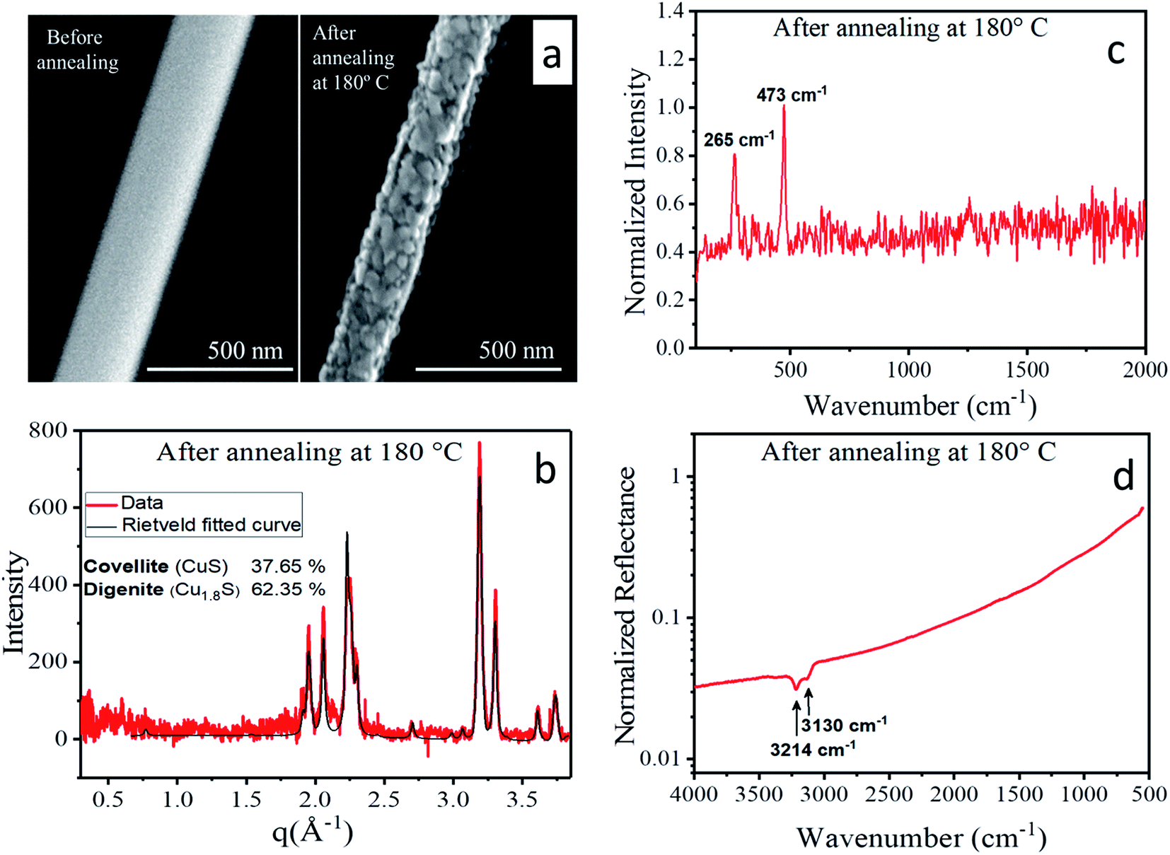 | ||
| Fig. 10 (a) Scanning electron micrographs of a CTC nanowire before (left) and after (right) annealing at 180 °C, (b) X-ray diffraction pattern (red line) with Rietveld fit (black line) (c) Raman and (d) FTIR spectra of the nanowires after annealing at 180 °C. | ||
Conclusions
In summary, we synthesized copper thiourea complex (CTC) nanowires by the electrochemical pulse deposition technique. EDS measurements confirmed that the compositional elements are C, N, O, S, Cl and Cu. Our HRTEM investigation showed that the nanowires are polycrystalline. The combination of these results with data obtained from X-ray diffraction, FTIR, Raman and optical absorption spectroscopy pointed towards the formation of the complex ([Cu(tu)]Cl·½H2O). Comparison with literature suggested the described formation mechanism of CTCs instead of copper sulfide under the applied synthesis condition. By choosing a suitable pulse structure, phase-pure and high aspect ratio nanowires were grown. The existence of a direct band gap of 3.65 eV qualifies the synthesized CTC for the class of wide band gap materials. Thermal treatment at 180 °C fully converts the CTC nanowires into copper sulfide. In general, the demonstrated electrochemical synthesis of copper thiourea complex nanowires as a precursor for copper sulfide nanocrystals potentially serves as a step towards an optimized processing technology for copper sulfide based optoelectronic devices and solar cells.Conflicts of interest
There is no conflict of interest to declare.Acknowledgements
We acknowledge DESY (Hamburg, Germany), a member of the Helmholtz Association HGF, for the provision of experimental facilities. Parts of this research were carried out at PETRA III and DESY NanoLab. We acknowledge the use of the FIB dual beam instrument granted by BMBF under grant no. 5K13WC3 (PT-DESY). A. S., M. K. S. and G. M. acknowledge Department of Science and Technology (DST) of India for the financial support for beamtime at PETRA III (proposal I-20160396).Notes and references
- C.-H. Lai, M.-Y. Lu and L.-J. Chen, J. Mater. Chem., 2012, 22, 19–30 RSC.
- Z.-H. Wang, D.-Y. Geng, Y.-J. Zhang and Z.-D. Zhang, Mater. Chem. Phys., 2010, 122, 241–245 CrossRef CAS.
- D. Milliron, S. M. Hughes, Y. Cui, L. Manna, J. Li, L. W. Wang and A. P. Alivisatos, Nature, 2004, 430, 190–195 CrossRef CAS.
- H. Yang, L. A. Jauregui, G. Zhang, Y. P. Chen and Y. Wu, Nano Lett., 2012, 12, 540–545 CrossRef CAS.
- S. W. Lee, Y. Yang, H.-W. Lee, H. Ghasemi, D. Kraemer, G. Chen and Y. Cui, Nat. Commun., 2014, 5, 3942 CrossRef CAS.
- M. Page, O. Niitsoo, Y. Itzhaik, D. Cahen and G. Hodes, Energy Environ. Sci., 2009, 2, 220–223 RSC.
- Y. Yao, B. P. Zhang, J. Pei, Y. C. Liu and J. F. Li, J. Mater. Chem. C, 2017, 5, 7845–7852 RSC.
- X. Li, C. Hu, X. Kang, Q. Len, Y. Xi, K. Zhang and H. Liu, J. Mater. Chem. A, 2013, 1, 13721–13726 RSC.
- P. D. Tran, M. Nguyen, S. S. Pramana, A. Bhattacharjee, S. Y. Chiam, J. Fize, M. J. Field, V. Artero, L. H. Wong, J. Loo and J. Barber, Energy Environ. Sci., 2012, 5, 8912–8916 RSC.
- M. Pal, N. R. Mathews, E. Sanchez-Mora, U. Pal, F. Paraguay-Delgado and X. Mathew, J. Nanopart. Res., 2015, 17, 301 CrossRef.
- S. B. Aziz, R. T. Abdulwahid, H. A. Rsaul and H. M. Ahmed, J. Mater. Sci.: Mater. Electron., 2016, 27, 4163–4171 CrossRef CAS.
- V. B. Llorente, V. M. Dzhagan, N. Gaponik, R. A. Iglesias, D. R. T. Zahn and V. Lesnyak, J. Phys. Chem. C, 2017, 121, 18244–18253 CrossRef CAS.
- S. K. Han, C. Gu, S. Zhao, S. Xu, M. Gong, Z. Li and S. H. Yu, J. Am. Chem. Soc., 2016, 138, 12913–12919 CrossRef CAS.
- Y. Lou, X. Chen, A. C. Samia and C. Burda, J. Phys. Chem. B, 2003, 107, 12431–12437 CrossRef CAS.
- T. C. Caesar-Tonthat, F. Van Ommen, G. G. Geesey and J. M. Henson, Appl. Environ. Microbiol., 1995, 61, 1968–1975 CAS.
- L. Guo, I. Panderi, D. D. Yan, K. Szulak, Y. Li, Y. T. Chen, H. Ma, D. B. Niesen, N. Seeram, A. Ahmed, B. Yan, D. Pantazatos and W. Lu, ACS Nano, 2013, 7, 8780–8793 CrossRef CAS.
- W. Feng, W. Nie, Y. Cheng, X. Zhou, L. Chen, K. Qiu, Z. Chen, M. Zhu and C. He, Nanomedicine, 2015, 11, 901–912 CrossRef CAS.
- K. Ahlman, R.-S. Koskela, P. Kuikka, M. Koponen and M. Annanmäki, Am. J. Ind. Med., 1991, 19, 603–617 CrossRef CAS.
- Z. Wang, P. Huang, O. Jacobson, Z. Wang, Y. Liu, L. Lin, J. Lin, N. Lu, H. Zhang, R. Tian, G. Niu, G. Liu and X. Chen, ACS Nano, 2016, 10, 3453–3460 CrossRef CAS.
- L. Guo, D. D. Yan, D. Yang, Y. Li, X. Wang, O. Zalewski, B. Yan and W. Lu, ACS Nano, 2014, 8, 5670–5681 CrossRef CAS.
- S. Goel, F. Chen and W. Cai, Small, 2014, 10, 631–645 CrossRef CAS.
- C. Tan, Y. Zhu, R. Lu, P. Xue, C. Bao, X. Liu, Z. Fei and Y. Zhao, Mater. Chem. Phys., 2005, 91, 44–47 CrossRef CAS.
- A. Ghahremaninezhad, E. Asselin and D. G. Dixon, J. Phys. Chem. C, 2011, 115, 9320–9334 CrossRef CAS.
- S. K. Maji, N. Mukherjee, A. K. Dutta, D. N. Srivastava, P. Paul, B. Karmakar, A. Mondal and B. Adhikary, Mater. Chem. Phys., 2011, 130, 392–397 CrossRef CAS.
- G. Ma, Y. Zhou, X. Li, K. Sun, S. Liu, J. Hu and N. A. Kotov, ACS Nano, 2013, 7, 9010–9018 CrossRef CAS.
- H. T. Zhang, G. Wu and X. H. Chen, Mater. Chem. Phys., 2006, 98, 298–303 CrossRef CAS.
- C. Wu, J. Bin Shi, C. J. Chen, Y. C. Chen, Y. T. Lin, P. F. Wu and S. Y. Wei, Mater. Lett., 2008, 62, 1074–1077 CrossRef CAS.
- Y. Huang, H. Xiao, S. Chen and C. Wang, Ceram. Int., 2009, 35, 905–907 CrossRef CAS.
- S. S. Dhasade, J. S. Patil, S. H. Han, M. C. Rath and V. J. Fulari, Mater. Lett., 2013, 90, 138–141 CrossRef CAS.
- T. H. Larsen, M. Sigman, A. Ghezelbash, R. C. Doty and B. A. Korgel, J. Am. Chem. Soc., 2003, 125, 5638–5639 CrossRef CAS.
- M. B. Sigman, A. Ghezelbash, T. Hanrath, A. E. Saunders, F. Lee and B. A. Korgel, J. Am. Chem. Soc., 2003, 125, 16050–16057 CrossRef CAS.
- U. Shamraiz, R. A. Hussain and A. Badshah, J. Solid State Chem., 2016, 238, 25–40 CrossRef CAS.
- N. Pradhan, B. Katz and S. Efrima, J. Phys. Chem. B, 2003, 107, 13843–13854 CrossRef CAS.
- M. P. Hendricks, M. P. Campos, G. T. Cleveland, I. J. La Plante and J. S. Owen, Science, 2015, 348, 1226–1230 CrossRef CAS.
- G. Mondal, M. Acharjya, A. Santra, P. Bera, S. Jana, N. C. Pramanik, A. Mondal and P. Bera, New J. Chem., 2015, 39, 9487–9496 RSC.
- J. Flor, S. A. Marques De Lima and M. R. Davolos, Progress in Colloid and Polymer Science, Springer Berlin Heidelberg, Berlin, Heidelberg, 2004, vol. 128, pp. 239–243 Search PubMed.
- K. Nayan Sharma, H. Joshi, O. Prakash, A. K. Sharma, R. Bhaskar and A. K. Singh, Eur. J. Inorg. Chem., 2015, 2015, 4829–4838 CrossRef CAS.
- P. Kumar, M. Gusain and R. Nagarajan, Inorg. Chem., 2011, 50, 3065–3070 CrossRef CAS.
- J. Liu and D. Xue, J. Mater. Chem., 2011, 21, 223–228 RSC.
- G. Zayed and J. Winter, Appl. Microbiol. Biotechnol., 2000, 53, 726–731 CrossRef CAS.
- K. Woo, Y. Kim and J. Moon, Energy Environ. Sci., 2012, 5, 5340–5345 RSC.
- P. Kubelka and F. Munk, Z. Tech. Phys., 1931, 12, 593–601 Search PubMed.
- J. Madarász, M. Krunks, L. Niinistö and G. Pokol, J. Therm. Anal. Calorim., 2015, 120, 189–199 CrossRef.
- C. Coughlan, M. Ibáñez, O. Dobrozhan, A. Singh, A. Cabot and K. M. Ryan, Chem. Rev., 2017, 117, 5865–6109 CrossRef CAS.
- M. Krunks, T. Leskelä, R. Mannonen and L. Niinistö, J. Therm. Anal. Calorim., 1998, 53, 355–364 CrossRef CAS.
- P. Bombicz, I. Mutikainen, M. Krunks, T. Leskelä, J. Madarász and L. Niinistö, Inorg. Chim. Acta, 2004, 357, 513–525 CrossRef CAS.
- D. Han, Y. Zhang, Y. Shen, Z. Wang and L. Niu, Mater. Lett., 2007, 61, 3632–3634 CrossRef CAS.
- I. V. Mironov and L. D. Tsvelodub, J. Solution Chem., 1996, 25, 315–325 CrossRef CAS.
- A. E. Bolzán, A. S. M. A. Haseeb, P. L. Schilardi, R. C. V. Piatti, R. C. Salvarezza and A. J. Arvia, J. Electroanal. Chem., 2001, 500, 533–542 CrossRef.
- A. S. M. A. Haseeb, P. L. Schilardi, A. E. Bolzan, R. C. V. Piatti, R. C. Salvarezza and A. J. Arvia, J. Electroanal. Chem., 2001, 500, 543–553 CrossRef CAS.
- G. Fabricius, K. Kontturi and G. Sundholm, Electrochim. Acta, 1994, 39, 2353–2357 CrossRef CAS.
- W. Schwarzacher, Electrochem. Soc. Interface, 2006, 15, 32–35 CAS.
- M. Quinet, F. Lallemand, L. Ricq, J. Y. Hihn, P. Delobelle, C. Arnould and Z. Mekhalif, Electrochim. Acta, 2009, 54, 1529–1536 CrossRef CAS.
- D. F. Suarez and F. A. Olson, J. Appl. Electrochem., 1992, 22, 1002–1010 CrossRef CAS.
- A. Szymaszek, J. Biernat and L. Pajdowski, Electrochim. Acta, 1977, 22, 359–364 CrossRef CAS.
- G. Horányi, E. M. Rizmayer and P. Joó, J. Electroanal. Chem. Interfacial Electrochem., 1983, 149, 221–235 CrossRef.
- D. Vasquez Moll, M. R. G. De Chialvo, R. C. Salvarezza and A. J. Arvia, Electrochim. Acta, 1985, 30, 1011–1016 CrossRef.
- M. L. Hartsell and L. S. Plano, J. Inst. Met., 1994, 9, 921–926 CAS.
- A. Stierle, T. F. Keller, H. Noei, V. Vonk and R. Roehlsberger, Journal of Large-Scale Research Facilities, 2016, 2, A76 CrossRef.
- D. E. Newbury and N. W. M. Ritchie, J. Mater. Sci., 2014, 50, 493–518 CrossRef.
- International Center for Diffraction Data, Powder Diffraction File database (PDF-4) 00-053-0121 Search PubMed.
- International Center for Diffraction Data, Powder Diffraction File database (PDF-4) 00-09-0328 Search PubMed.
- International Center for Diffraction Data, Powder Diffraction File database (PDF-4) 00-065-9637 Search PubMed.
- M. Krunks, E. Mellikov and O. Bijakina, Phys. Scr., 1997, T69, 189–192 CrossRef CAS.
- G. M. S. El-Bahy, B. A. El-Sayed and A. A. Shabana, Vib. Spectrosc., 2003, 31, 101–107 CrossRef CAS.
- D. Han, W. Yang, F. Gu and Z. Wang, Sens. Actuators, B, 2018, 255, 1139–1146 CrossRef CAS.
- M. Ishii, K. Shibata and H. Nozaki, J. Solid State Chem., 1993, 105, 504–511 CrossRef CAS.
- G. Kortüm, Reflectance Spectroscopy, Springer Berlin Heidelberg, Berlin, Heidelberg, 1969 Search PubMed.
- J. Tauc, in Optical Properties of Solids, Springer US, Boston, MA, 1969, vol. 3, pp. 123–136 Search PubMed.
- A. C. Sajikumar and V. T. Jisha, Int. J. Phys. Appl., 2016, 8, 45–51 Search PubMed.
- T. C. S. Girisun, S. Dhanuskodi, J. Phillip, P. Predeep, M. Thakur and M. K. R. Varma, AIP Conf. Proc., 2011, 1391, 535–537 CrossRef CAS.
- S. Gopinath, S. Barathan and R. Rajasekaran, Adv. Mater. Res., 2012, 584, 112–115 CAS.
- K. Meena, K. Muthu, M. Rajasekar, V. Meenatchi, S. P. Meenakshisundaram and S. C. Mojumdar, J. Therm. Anal. Calorim., 2013, 112, 1077–1082 CrossRef CAS.
- P. Cofré and A. Bustos, J. Appl. Electrochem., 1994, 24, 564–568 CrossRef.
- H. M. Ratajczak and L. Pajdowski, J. Inorg. Nucl. Chem., 1974, 36, 459–461 CrossRef CAS.
- E. M. Khairy and N. A. Darwish, Corros. Sci., 1973, 13, 149–164 CrossRef CAS.
- O. E. Piro, R. C. V. Piatti, A. E. Bolzán, R. C. Salvarezza and A. J. Arvia, Acta Crystallogr., Sect. B: Struct. Sci., 2000, 56, 993–997 CrossRef.
- International Center for Diffraction Data, Powder Diffraction File database (PDF-4) 04-003-4437 Search PubMed.
- International Center for Diffraction Data, Powder Diffraction File database (PDF-4) 04-001-1461 Search PubMed.
Footnote |
| † Electronic supplementary information (ESI) available. See DOI: 10.1039/c9ra04293h |
| This journal is © The Royal Society of Chemistry 2019 |